EP0874459A2 - D-Flipflop-Schaltung - Google Patents
D-Flipflop-Schaltung Download PDFInfo
- Publication number
- EP0874459A2 EP0874459A2 EP98107134A EP98107134A EP0874459A2 EP 0874459 A2 EP0874459 A2 EP 0874459A2 EP 98107134 A EP98107134 A EP 98107134A EP 98107134 A EP98107134 A EP 98107134A EP 0874459 A2 EP0874459 A2 EP 0874459A2
- Authority
- EP
- European Patent Office
- Prior art keywords
- circuit
- differential
- current
- data
- differential circuit
- Prior art date
- Legal status (The legal status is an assumption and is not a legal conclusion. Google has not performed a legal analysis and makes no representation as to the accuracy of the status listed.)
- Withdrawn
Links
Images


Classifications
-
- H—ELECTRICITY
- H03—ELECTRONIC CIRCUITRY
- H03K—PULSE TECHNIQUE
- H03K3/00—Circuits for generating electric pulses; Monostable, bistable or multistable circuits
- H03K3/02—Generators characterised by the type of circuit or by the means used for producing pulses
- H03K3/353—Generators characterised by the type of circuit or by the means used for producing pulses by the use, as active elements, of field-effect transistors with internal or external positive feedback
- H03K3/356—Bistable circuits
- H03K3/3562—Bistable circuits of the primary-secondary type
-
- H—ELECTRICITY
- H03—ELECTRONIC CIRCUITRY
- H03K—PULSE TECHNIQUE
- H03K3/00—Circuits for generating electric pulses; Monostable, bistable or multistable circuits
- H03K3/02—Generators characterised by the type of circuit or by the means used for producing pulses
- H03K3/26—Generators characterised by the type of circuit or by the means used for producing pulses by the use, as active elements, of bipolar transistors with internal or external positive feedback
- H03K3/28—Generators characterised by the type of circuit or by the means used for producing pulses by the use, as active elements, of bipolar transistors with internal or external positive feedback using means other than a transformer for feedback
- H03K3/281—Generators characterised by the type of circuit or by the means used for producing pulses by the use, as active elements, of bipolar transistors with internal or external positive feedback using means other than a transformer for feedback using at least two transistors so coupled that the input of one is derived from the output of another, e.g. multivibrator
- H03K3/286—Generators characterised by the type of circuit or by the means used for producing pulses by the use, as active elements, of bipolar transistors with internal or external positive feedback using means other than a transformer for feedback using at least two transistors so coupled that the input of one is derived from the output of another, e.g. multivibrator bistable
- H03K3/289—Generators characterised by the type of circuit or by the means used for producing pulses by the use, as active elements, of bipolar transistors with internal or external positive feedback using means other than a transformer for feedback using at least two transistors so coupled that the input of one is derived from the output of another, e.g. multivibrator bistable of the primary-secondary type
Definitions
- the present invention relates to a D-type flip-flop circuit.
- a master-slave type D-type flip-flop circuit composed of bipolar transistors (hereinafter referred to simply as a transistor) is being used.
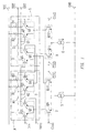
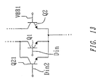
- FIG. 16 shows a structure of such a D-type flip-flop circuit wherein a master circuit 161 comprises a differential circuit 162 for inputting data, a differential circuit 163 for holding data, a current supplying circuit 164 for supplying a current to the differential circuits 162 and 163 and a switching circuit 165 for alternately supplying the current to the differential circuits 162 and 163.
- a master circuit 161 comprises a differential circuit 162 for inputting data, a differential circuit 163 for holding data, a current supplying circuit 164 for supplying a current to the differential circuits 162 and 163 and a switching circuit 165 for alternately supplying the current to the differential circuits 162 and 163.
- the differential circuit 162 comprises transistors q1 and q2 whose emitters are connected in common, whose bases receive data which are signals inverted from each other and whose collectors are set as outputs. It is noted that the collectors of these transistors q1 and q2 are connected to a source terminal VCC via resistors r1 and r2. While the differential circuit 162 receives input data which are signals inverted from each other via input terminals d1 and d2, also it may be available one in which one of the input terminals d1 and d2 is fixed to a reference potential.
- the differential circuit 163 comprises transistors q3 and q4 whose emitters are connected in common and whose bases and collectors are connected across each other.
- the current supplying circuit 164 comprises a transistor q5 which receives a current value setting signal from a current value setting terminal VCS at its base and whose emitter is connected to a source terminal GND.
- the switching circuit 165 comprises a pair of transistors q6 and q7 whose respective collectors are connected to emitter connecting points ce1 and ce2 of the respective differential circuits 162 and 163 and whose respective emitters are connected in common to a collector of the transistor q5 of the current supplying circuit 164.
- the transistors q6 and q7 turn on alternately and supply the currents to the differential circuits 162 and 163, respectively, by receiving clock signals which are inverted from each other at their bases via respective clock terminals cl1 and cl2.
- a slave circuit 166 is also constructed in the same manner with the master circuit 161.
- Bases of transistors q8 and q9 of a differential circuit 167 for inputting data in the slave circuit 166 are connected to the collectors of the transistors q3 and q4 of the differential circuit 163 in the master circuit 161, respectively, to receive the output data held in the differential circuit 163.
- collectors of transistors q10 and q11 of a fourth differential circuit 168 for holding data are set as output terminals.
- a base of a transistor q12 of a current supplying circuit 169 is connected to the current value setting terminal VCS in common with the base of the transistor q5 of the current supplying circuit 164.
- a switching circuit 170 comprises transistors q13 and q14 whose respective collectors are connected to emitter connecting points ce3 and ce4 of the respective differential circuits 167 and 168 and whose respective emitters are connected in common to a collector of the transistor q12 of the current supplying circuit 169.
- the transistors q13 and q14 turn on alternately and supply the currents to the differential circuits 167 and 168, respectively, by receiving the clock signals at their bases via the clock terminals cl2 and cl1.
- the first differential circuit 162 writes input data from the input terminals d1 and d2 in correspondence to "H", which means “high state” hereinafter, of the clock signal of the clock terminal c11 and in the same time, the differential circuit 168 holds output data of the differential circuit 167.
- the differential circuit 163 holds the output data of the differential circuit 163 and in the same time, the differential circuit 167 writes in the output data of the differential circuit 162.
- the switching circuits 165 and 170 operate as follows. Timing of ON/OFF of the transistor q6 is simultaneous with that of the transistor q14 and timing of ON/OFF of the transistor q7 is simultaneous with that of the transistor q13. When the transistors q6 and q14 are ON, the transistors q7 and q13 are OFF and vice versa. They are turned ON/OFF simultaneously.
- ON/OFF used here that although it is unable to clearly distinguish ON/OFF when frequency increases, it is expressed as "the transistor q6 is ON and the transistor q7 is OFF” in a state that "the transistor q6 turns ON strongly as compared to the transistor q7" even when the transistors q6 and q7 turn ON in the same time for example. The same can be said also in the embodiments described later.
- the D-type flip-flop circuit shown in FIG. 16 has had a trouble in its operation in high frequency because it has not been able to compensate a propagation delay time due to its structure.
- the differential circuit 163 continues to hold the old data for a while even when the transistor q7 turns OFF and the transistor q6 turns ON in the same time because of the propagation time. Therefore, the new input data takes an extra load for inverting the old data.
- it is possible to write the data in a shorter time if it is written in a state in which there is no old data because it is not necessary to invert the data and it requires only a load for writing the data. Actually it takes a time to write the data because of the extra load and the writing operation cannot follow the clock signal as operating frequency increases.
- a source for supplying a current to respective differential circuits for inputting and holding data of a master circuit and a slave circuit is divided into a first current supplying circuit and a second current supplying circuit, respectively, and timing for supplying the current to the respective differential circuits for inputting and holding data is controlled by first and second clock signals. Then timing for writing input data and timing for holding data are optimized by arranging the first clock signal so as to have a predetermined delay with respect to the second clock signal, thus improving the D-type flip-flop circuit with respect to operating frequency thereof. In addition to that, the D-type flip-flop circuit is improved with respect to the operating frequency further by optimizing the value of current supplied to the respective differential circuits.
- the D-type flip-flop circuit comprises a master circuit having a first differential circuit for generating output data corresponding to input data and a second differential circuit for holding and outputting the output data from the first differential circuit; a slave circuit having a third differential circuit for generating second output data corresponding to the output data from the second differential circuit of the master circuit and a fourth differential circuit for holding and outputting the second output data from the third differential circuit; a first current supplying circuit for supplying a first current to the first and third differential circuits; a second current supplying circuit for supplying a second current to the second and fourth differential circuits; a first switching circuit for connecting the first and third differential circuits alternately to the first current supplying circuit by receiving a first clock signal; and a second switching circuit for connecting the second and fourth differential circuits alternately to the second current supplying circuit by receiving a second clock signal; and the first clock signal has a predetermined delay with respect to the second clock signal.
- the value of the second current is smaller than the value of the first current.
- the second switching circuit starts to supply the current to the second differential circuit or the fourth differential circuit preceding to stopping to supply the current to the first differential circuit or the third differential circuit and stops to supply the current to the second differential circuit or the fourth differential circuit preceding to starting to supply the current to the first differential circuit or the third differential circuit in accordance to the second clock signal.
- first and second emitter-follower circuits are provided between an output terminal of the first differential circuit and an input terminal of the second differential circuit and between an output terminal of the third differential circuit and an input terminal of the fourth differential circuit, respectively, and a signal which goes through the first emitter-follower circuit is input to the input terminal of the second differential circuit and a signal which goes through the second emitter-follower circuit is output.
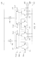
- a D-type flip-flop circuit according to a first embodiment of the present invention will be explained below.
- FIG. 1 is a circuit diagram showing a structure of the D-type flip-flop circuit of the present embodiment. The structure thereof will be explained at first with reference to the figure.
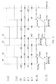
- a master circuit M comprises a first differential circuit 1 for inputting data and a second differential circuit 2 for holding data.
- a slave circuit S comprises a third differential circuit 3 for inputting data and a fourth differential circuit 4 for holding data.
- the first differential circuit comprises transistors Q1 and Q2 whose emitters are connected in common, whose collectors are connected to a source terminal VCC via resistors R1 and R2, respectively, and whose bases receive signals from terminals Din and VBB1 as data, respectively.
- the signal from the terminal VBB1 may be what is inverted from that from the terminal Din or one of them may be a reference potential.
- a reference potential is applied to the terminal VBB1 and a current is being supplied to the first differential circuit.
- the transistors Q1 and Q2 are turned ON and OFF, respectively, when the signal Din turns to "H” and are turned OFF and ON when the signal turns to "L” which means “Low state” hereinafter.
- the transistors Q1 and Q2 are turned ON/OFF in response to the signal of the terminal Din, so voltage drops due to the respective resistors R1 and R2 from the potential of the source terminal VCC occur as outputs at the collectors, respectively.
- the second differential circuit 2 comprises transistors Q3 and Q4 whose emitters are connected in common and whose bases and collectors are connected across each other.
- the collector of the transistor Q3 and the base of the transistor Q4 receive the data on the terminal M1 and the collector of the transistor Q4 and the base of the transistor Q3 receive the data on the terminal M2, thus holding and outputting the data while the current is being supplied.
- a third differential circuit 3 and a fourth differential circuit 4 of the slave circuit S are constructed in the same manner with the first differential circuit 1 and the second differential circuit 2, respectively.
- Bases of the transistors Q5 and Q6 of the third differential circuit 3 are connected with the terminals M2 and M1, respectively, to receive the respective data and to write output data corresponding to the output data from the second differential circuit 2 to terminals S1 and S2 connected to the respective collectors.
- Collectors of transistors Q7 and Q8 of the fourth differential circuit 4 are connected respectively with the terminals S1 and S2 which are provided with output terminals OUT and OUT, respectively. It is noted that the terminals S1 and S2 are connected to the source terminal VCC via resistors R3 and R4.
- a first current supplying circuit 5 supplies a current for the first and third differential circuits 1 and 3 and a second current supplying circuit 6 supplies a current for the second and fourth differential circuits 2 and 4.
- these circuits are constant-current circuits comprising transistors and resistors similarly to the current supplying circuit shown in the aforementioned prior art example, the present invention is not limited only to them and one which is connected directly to a source terminal GND via a resistor may be adopted.
- a switching circuit 7 is a differential circuit comprising transistors Q9 and Q10 whose emitters are connected in common to the first current supplying circuit 5, whose collectors are connected to emitter connecting points of the respective transistors of the first differential circuits 1 and 3 and whose bases are connected to clock terminals Cin1 and Cin1 to receive a first clock signal and its inverted signal (or a reference potential) to supply the current alternately to the first and third differential circuits 1 and 3.
- a switching circuit 8 is a differential circuit comprising transistors Q11 and 12 whose emitters are connected in common to the second current supplying circuit 6, whose collectors are connected to emitter connecting points of the respective transistors of the second and fourth differential circuits 2 and 4 and whose bases are connected to clock terminals Cin2 and Cin2 to receive a second clock signal and its inverted signal (or a reference potential) to supply the current alternately to the second and fourth differential circuits 2 and 4.
- the first clock signal is arranged so as to have a predetermined delay with respect to the second clock signal.
- a load in inverting data is lightened by finishing the data holding operation of the second and fourth differential circuits 2 and 4 earlier than causing the first and third differential circuits 1 and 3 to perform the writing operation.
- the inverting and writing operations during writing may be also enhanced by starting the holding operation of the second and fourth differential circuits 2 and 4 just before finishing the writing operation of the first and third differential circuits 1 and 3.
- Such a delay time is set by each circuit component and the like.
- the 1/2 frequency dividing circuit shown in FIG. 2 is what the terminal Din is connected with the output terminal OUT and the terminal VBB1 is connected with the terminal OUT in the D-type flip-flop circuit shown in FIG. 1. Further, a terminal VBB2 is connected with the clock terminals Cin1 and Cin2 to apply a common reference potential.
- Cin1 and Cin2 in FIG. 3 represent first and second clock signals of the clock terminals Cin1 and Cin2, Q9 through Q12 represent ON/OFF states of the respective transistors Q9 through Q12 and M1, M2, S1 and S2 represent data writing and holding states at terminals M1 and M2 of the master circuit M and at terminals S1 and S2 of the slave circuit S, respectively.
- the transistors Q11 and Q12 are turned OFF and ON, respectively, stopping to supply the current from the second current supplying circuit 6 to the second differential circuit 2, and the data held in the terminals M1 and M2 are going to be vanished. Further, as the transistor Q12 is turned ON, the current is started to be supplied from the second current supplying circuit 6 to the fourth differential circuit 4, So the operation for holding data in the terminals S1 and S2 is started.
- the transistors Q9 and Q10 of the first switching circuit 7 are turned ON and OFF, respectively, thus starting to supply the current from the first current supplying circuit 5 to the first differential circuit 1 and stopping to supply the current from the first current supplying circuit 5 to the third differential circuit 3.
- the data of the terminals S1 and S2 of the slave circuit S have been transmitted to the first differential circuit 1, so that the operation for writing them to the terminals M1 and M2 is started. For instance, when data "H” and "L” have been held in the terminals M1 and M2, an operation for inverting them is carried out by receiving the data of the terminals S1 and S2.
- the load of the inverting operation at timing t1 is small, i.e. it becomes possible to write quickly.
- the writing operation of the third differential circuit 3 stops as the first differential circuit 1 starts to write.
- the transistors Q11 and Q12 of the second switching circuit 8 are turned ON and OFF, respectively, starting to supply the current from the second current supplying circuit 6 to the second differential circuit 2 and stopping to supply the current to the fourth differential circuit 4.
- the second differential circuit 2 starts to hold the data and, this holding operation and the writing operation of the first differential circuit 1 combine to write the data strongly to the terminals M1 and M2. In other words, the same data is written doubly.
- the fourth differential circuit 4 stops the data holding operation and the data held in the terminals S1 and S2 are going to be vanished.
- the writing operation can be performed steadily because the old data is vanished before the new data is written both in the master circuit M and the slave circuit S and the transmitting side writes the same data doubly.
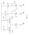
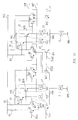
- a circuit as shown in FIG. 4 is used for examples as such a delay stage. It is constructed as a differential circuit comprising transistors Q13 and Q14 whose emitters are connected commonly to a current supplying circuit 9, whose collectors are connected to the source terminal VCC via resistors R5 and R6 and whose bases are applied with the second clock signal and its inverted signal.
- a connecting point of the collector of the transistor Q14 and the resistor R6 is connected to a base of a transistor Q15 and an amplifier circuit (emitter-follower circuit) composed of the transistor Q15 and a current supplying circuit 10 generates a signal from the terminal Cin1 as the first clock signal by receiving the state of the connecting point of the collector and the resistor.
- a connecting point of the collector of the transistor Q13 and the resistor R5 is connected to a base of a transistor Q16 and an amplifier circuit (emitter-follower circuit) composed of the transistor Q16 and a current supplying circuit 11 generates an inverted signal of the first clock signal from the terminal Cin1 by receiving the state of the connecting point of the collector and the resistor. That is, the delay between the first and second clock signals is decided by setting the delay of these amplifier circuits.
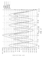
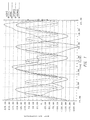
- FIGs. 6 and 7 are waveform charts when the 1/2 frequency dividing circuits in FIGs. 2 and 5 are operated with a clock signal of 1.25 GHz.
- a solid line V[M1] in FIG. 6 represents an amplitude of voltage at the terminal M1 in FIG. 2
- an alternate dashed line V[CIN1] represents the first clock signal
- a dotted line V[CIN2] represents the second clock signal
- a broken line V[M3] represents an amplitude of voltage at the terminal M3 in FIG. 5.
- a solid line V[S1] in FIG. 7 represents an amplitude of voltage at the terminal S1 in FIG.
- FIG. 8 shows a case when the 1/2 frequency dividing circuit is operated with a clock signal of 1.1 GHz.
- This chart shows a comparative result when the 1/2 frequency dividing circuit of the present embodiment as well as that of the prior art both follow the clock signal in the same manner. It can be seen from the result of this chart that the 1/2 frequency dividing circuit of the present embodiment can obtain an output having a clearer waveform having no distortion.
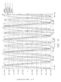
- FIG. 9 shows a case when the 1/2 frequency dividing circuit of the present embodiment is operated with a clock signal of 1.4 GHz. As shown in the chart, even the circuit of the present embodiment cannot follow such clock signal in this case.
- the present invention is not limited only to the case when the value of the current of the first current supplying circuit 5 is equalized with that of the second current supplying circuit 6. Because it requires less value of current on the level which will not vanish data in holding data like writing data which is not involved with the inverting operation, it is possible to increase operating frequency and to lessen power consumption by reducing the value of the current of the second current supplying circuit 6 to be less than that of the first current supplying circuit 5. The value of the current may be reduced by 20 % in the case of FIG. 10.
- the 1/2 frequency dividing circuit of the present embodiment operates even with the clock signal of 1.4 GHz as shown in FIG. 11.
- This arrangement excels in that a higher amplitude of voltage can be obtained as compared to the case when the power consumption is lowered.
- the simulation shown in FIG. 11 has been carried out by setting the value of the current of the first current supplying circuit 5 at 60 ⁇ A and that of the second current supplying circuit at 40 ⁇ A.
- the present embodiment allows the operating frequency to be increased and the value of power consumption to be reduced by setting the value of the current of the second current supplying circuit 6 to be less than that of the first current supplying circuit 5. It is noted that under the conditions of the above-mentioned simulations, it has been possible to set the delay of the first clock signal with respect to the second clock signal at 40 to 120 degrees, or preferably 60 to 90 degrees, in terms of a phase lag.
- emitter-follower circuits 12 and 13 are provided between the first differential circuit 1 and the second differential circuit 2 and emitter-follower circuits 14 and 15 are provided between the third differential circuit 3 and the fourth differential circuit 4. That is, although there has been a case when signals having a large amplitude are required depending on the latter circuit using the signals of the terminals S1 and S2 in the circuit shown in FIG.
- the emitter-follower circuits 12 through 15 are provided in the present embodiment.
- the emitter-follower circuit 12 comprises a transistor Q17 and a current supplying circuit 16.
- a base of the transistor Q17 is connected to the collector of the transistor Q1, a collector thereof is connected to the source terminal VCC and an emitter thereof is connected to the current supplying circuit 16 as well as to the base of the transistor Q4.
- the emitter-follower circuit 13 comprises a transistor Q18 and a current supplying circuit 17.
- a base of the transistor Q18 is connected with the collector of the transistor Q2, a collector thereof is connected with the source terminal VCC and an emitter thereof is connected with the current supplying circuit 17 as well as with the base of the transistor Q3.
- the respective holding routes contain the emitter-follower circuits, so that one stage of the base voltage VBE may be dropped between the first differential circuit 1 and the second differential circuit 2, eliminating the above-mentioned trouble.
- the output to the third differential circuit 3 is sent from a connecting point of the transistor Q17 and the current supplying circuit 16 and a connecting point of the transistor Q18 and the current supplying circuit 17.
- the emitter-follower circuits 14 and 15 also respectively comprise transistors Q19 and Q20 and current supplying circuits 18 and 19 each connected in the same manner. While an operation of the present embodiment will not be described specifically in detail, the present embodiment shows almost the same action and effect with those of the first embodiment. Further, because the emitter-follower circuits 12 through 15 are provided, an output having a large amplitude may be sent to the latter circuits.
- the present invention is not limited only to such a case.
- FIG. 14 shows a circuit in which the pnp-type bipolar transistors are applied to the D-type flip-flop circuit shown in FIG. 2.
- the circuit has the similar connection, though the polarity of the power and current sources are inverted.
- the circuit comprises first through fourth differential circuits 141 through 144, first and second current supplying circuits 145 and 146 and first and second switching circuits 147 and 148. It is noted that the data input terminal Din, the clock terminal Cin1, the output terminal OUT and the like are shown in the same manner with those shown in FIG. 2.
- the inventive circuit may be constructed also by using MOS transistors, instead of the bipolar transistors.
- FIG. 15 shows a case when the circuit is constructed by using N channel MOS transistors.
- the circuit comprises first through fourth differential circuits 151 through 154, first and second current supplying circuits 155 and 156 and first and second switching circuits 157 and 158.
- the data input terminal Din, the clock terminal Cin1, the output terminal OUT and the like are shown in the same manner with those shown in FIG. 2.
- the inventive circuit may be constructed by using P channel MOS transistors, instead of the N channel MOS transistors, also in the circuit composed of the MOS transistors in FIG. 15.
- the circuit has the same connection with that composed of the N channel MOS transistors, though the polarity of the power and current sources are inverted, similarly to the above-mentioned case of the bipolar transistors.
- the operation timing of the differential circuits for inputting data and for holding data is optimized by dividing the current supplying source to the respective two differential circuits for inputting data (first and third differential circuits) and for holding data (second and fourth differential circuits) of the master circuit and slave circuit, by controlling the timing for supplying the current separately by the first and second clock signals and by arranging the first clock signal so as to have the predetermined delay with respect to the second clock signal. Accordingly, the remarkable effects can be obtained in the aspects of the operating frequency, the waveform in operating in high frequency and the ability for transmitting data. In addition to that, it is possible to increase the operating frequency further and to lower the power consumption by setting the value of the current supplied to the second and fourth differential circuits to be less than that supplied to the first and third differential circuits.
Landscapes
- Engineering & Computer Science (AREA)
- Power Engineering (AREA)
- Logic Circuits (AREA)
- Dc Digital Transmission (AREA)
Applications Claiming Priority (3)
| Application Number | Priority Date | Filing Date | Title |
|---|---|---|---|
| JP10853697A JP3508085B2 (ja) | 1997-04-25 | 1997-04-25 | D型フリップフロップ回路 |
| JP10853697 | 1997-04-25 | ||
| JP108536/97 | 1997-04-25 |
Publications (2)
| Publication Number | Publication Date |
|---|---|
| EP0874459A2 true EP0874459A2 (de) | 1998-10-28 |
| EP0874459A3 EP0874459A3 (de) | 2001-02-14 |
Family
ID=14487305
Family Applications (1)
| Application Number | Title | Priority Date | Filing Date |
|---|---|---|---|
| EP98107134A Withdrawn EP0874459A3 (de) | 1997-04-25 | 1998-04-20 | D-Flipflop-Schaltung |
Country Status (3)
| Country | Link |
|---|---|
| US (1) | US6218878B1 (de) |
| EP (1) | EP0874459A3 (de) |
| JP (1) | JP3508085B2 (de) |
Cited By (3)
| Publication number | Priority date | Publication date | Assignee | Title |
|---|---|---|---|---|
| WO2004015864A3 (en) * | 2002-08-12 | 2004-07-15 | Sun Microsystems Inc | Clocked differential logic with sense amplifier |
| GB2367963B (en) * | 2000-08-09 | 2004-09-22 | Atmel Germany Gmbh | Method for increasing the cut-off frequency in flip-flops |
| WO2011036212A1 (en) * | 2009-09-24 | 2011-03-31 | Technische Universität Dresden | Static frequency divider circuitry |
Families Citing this family (18)
| Publication number | Priority date | Publication date | Assignee | Title |
|---|---|---|---|---|
| US6424194B1 (en) * | 1999-06-28 | 2002-07-23 | Broadcom Corporation | Current-controlled CMOS logic family |
| US6538486B1 (en) * | 2000-10-11 | 2003-03-25 | Lucent Technologies Inc. | Latch chain having improved sensitivity |
| US7212534B2 (en) | 2001-07-23 | 2007-05-01 | Broadcom Corporation | Flow based congestion control |
| US6501314B1 (en) * | 2002-03-06 | 2002-12-31 | Teradyne, Inc. | Programmable differential D flip-flop |
| US7295555B2 (en) | 2002-03-08 | 2007-11-13 | Broadcom Corporation | System and method for identifying upper layer protocol message boundaries |
| JP2004040301A (ja) * | 2002-07-01 | 2004-02-05 | Nec Corp | スタティック型フリップフロップ回路 |
| US7346701B2 (en) | 2002-08-30 | 2008-03-18 | Broadcom Corporation | System and method for TCP offload |
| US7934021B2 (en) | 2002-08-29 | 2011-04-26 | Broadcom Corporation | System and method for network interfacing |
| US8180928B2 (en) | 2002-08-30 | 2012-05-15 | Broadcom Corporation | Method and system for supporting read operations with CRC for iSCSI and iSCSI chimney |
| EP1554842A4 (de) | 2002-08-30 | 2010-01-27 | Corporation Broadcom | System und verfahren zum behandeln von ausserhalb der reihenfolge auftretenden rahmen |
| US7313623B2 (en) | 2002-08-30 | 2007-12-25 | Broadcom Corporation | System and method for TCP/IP offload independent of bandwidth delay product |
| DE102004009283B4 (de) * | 2004-02-26 | 2006-04-20 | Infineon Technologies Ag | Flip-Flop-Schaltungsanordnung und Verfahren zur Verarbeitung eines Signals |
| US7161395B2 (en) * | 2004-06-24 | 2007-01-09 | Stmicroelectronics, Inc. | Static frequency divider with low power supply |
| US7230459B2 (en) * | 2004-06-30 | 2007-06-12 | Stmicroelectronics, Inc. | Static frequency divider for microwave applications |
| US7705650B2 (en) * | 2007-08-14 | 2010-04-27 | Sony Corporation | System and method for effectively implementing an IQ generator |
| WO2012141008A1 (ja) * | 2011-04-11 | 2012-10-18 | 日本電気株式会社 | 半導体集積回路 |
| RU2693301C9 (ru) * | 2018-10-16 | 2020-03-11 | Федеральное государственное бюджетное образовательное учреждение высшего образования "Юго-Западный государственный университет" (ЮЗГУ) | Триггерный синхронный D триггер на полевых транзисторах |
| RU2693320C1 (ru) * | 2018-11-21 | 2019-07-02 | Федеральное государственное учреждение "Федеральный исследовательский центр "Информатика и управление" Российской академии наук" (ФИЦ ИУ РАН) | Самосинхронный динамический однотактный d-триггер с нулевым спейсером |
Family Cites Families (9)
| Publication number | Priority date | Publication date | Assignee | Title |
|---|---|---|---|---|
| DE2821231C2 (de) * | 1978-05-16 | 1980-01-24 | Siemens Ag, 1000 Berlin Und 8000 Muenchen | Master-Slave-Flipflop in Stromschalter-Technik |
| JPS5925421A (ja) * | 1982-08-03 | 1984-02-09 | Toshiba Corp | 同期式論理回路 |
| US4692641A (en) * | 1986-02-13 | 1987-09-08 | Burr-Brown Corporation | Level shifting circuitry for serial-to-parallel converter |
| JPH02292910A (ja) * | 1989-05-02 | 1990-12-04 | Sumitomo Electric Ind Ltd | マスタ・スレーブ型フリップ・フロップ回路 |
| US5172011A (en) * | 1989-06-30 | 1992-12-15 | Digital Equipment Corporation | Latch circuit and method with complementary clocking and level sensitive scan capability |
| US5239206A (en) * | 1990-03-06 | 1993-08-24 | Advanced Micro Devices, Inc. | Synchronous circuit with clock skew compensating function and circuits utilizing same |
| JP2747467B2 (ja) * | 1991-08-19 | 1998-05-06 | 日本電信電話株式会社 | スタティック型フリップフロップ回路 |
| JP2693329B2 (ja) * | 1991-10-15 | 1997-12-24 | 日本電信電話株式会社 | スタティック型フリップフロップ回路 |
| JP3539509B2 (ja) * | 1994-03-15 | 2004-07-07 | 株式会社ルネサステクノロジ | 電流切換型論理回路 |
-
1997
- 1997-04-25 JP JP10853697A patent/JP3508085B2/ja not_active Expired - Fee Related
-
1998
- 1998-04-16 US US09/061,528 patent/US6218878B1/en not_active Expired - Fee Related
- 1998-04-20 EP EP98107134A patent/EP0874459A3/de not_active Withdrawn
Cited By (3)
| Publication number | Priority date | Publication date | Assignee | Title |
|---|---|---|---|---|
| GB2367963B (en) * | 2000-08-09 | 2004-09-22 | Atmel Germany Gmbh | Method for increasing the cut-off frequency in flip-flops |
| WO2004015864A3 (en) * | 2002-08-12 | 2004-07-15 | Sun Microsystems Inc | Clocked differential logic with sense amplifier |
| WO2011036212A1 (en) * | 2009-09-24 | 2011-03-31 | Technische Universität Dresden | Static frequency divider circuitry |
Also Published As
| Publication number | Publication date |
|---|---|
| JPH10303707A (ja) | 1998-11-13 |
| US6218878B1 (en) | 2001-04-17 |
| EP0874459A3 (de) | 2001-02-14 |
| JP3508085B2 (ja) | 2004-03-22 |
Similar Documents
| Publication | Publication Date | Title |
|---|---|---|
| EP0874459A2 (de) | D-Flipflop-Schaltung | |
| JP3681497B2 (ja) | フリップフロップ回路、シフトレジスタ回路、直列−並列変換回路、並列−直列変換回路およびラッチ回路 | |
| JPH02141120A (ja) | 走査可能レジスタ/ラッチ回路 | |
| JPS5925421A (ja) | 同期式論理回路 | |
| US5359241A (en) | ECL circuit | |
| US4622475A (en) | Data storage element having input and output ports isolated from regenerative circuit | |
| US4727265A (en) | Semiconductor circuit having a current switch circuit which imparts a latch function to an input buffer for generating high amplitude signals | |
| US4626706A (en) | Digital signal level translation/master-slave flip flop with look-ahead | |
| JPS60254922A (ja) | 双対モ−ド論理回路 | |
| JP2990791B2 (ja) | コレクタドットアンド回路 | |
| US5396125A (en) | Current injection logic | |
| WO2001018962A1 (fr) | Circuit a bascule, et procede de maintien et de synchronisation de donnees utilisant un signal d'horloge | |
| JPH0584687B2 (de) | ||
| JP3872193B2 (ja) | D/aコンバータのメモリセル用回路装置 | |
| US5541545A (en) | High speed bipolar D latch circuit with reduced latch clocking output corruption | |
| JPS6316047B2 (de) | ||
| JP2776201B2 (ja) | フリップフロップ回路 | |
| JPS6135021A (ja) | ユニタリマルチプレクサーデコーダ回路 | |
| JP2663732B2 (ja) | 論理判定回路 | |
| JPH0537305A (ja) | ラツチ回路 | |
| JPS61176872A (ja) | 論理回路 | |
| KR19990029445A (ko) | 고속에서 동작가능한 이미터결합 논리회로 | |
| JP2965581B2 (ja) | カウンタ用電流切換型回路 | |
| JPH0715675B2 (ja) | シリアルインタ−フエ−ス回路 | |
| JPH0732357B2 (ja) | 論理レベル設定回路 |
Legal Events
| Date | Code | Title | Description |
|---|---|---|---|
| PUAI | Public reference made under article 153(3) epc to a published international application that has entered the european phase |
Free format text: ORIGINAL CODE: 0009012 |
|
| AK | Designated contracting states |
Kind code of ref document: A2 Designated state(s): DE FR GB |
|
| AX | Request for extension of the european patent |
Free format text: AL;LT;LV;MK;RO;SI |
|
| PUAL | Search report despatched |
Free format text: ORIGINAL CODE: 0009013 |
|
| AK | Designated contracting states |
Kind code of ref document: A3 Designated state(s): AT BE CH CY DE DK ES FI FR GB GR IE IT LI LU MC NL PT SE |
|
| AX | Request for extension of the european patent |
Free format text: AL;LT;LV;MK;RO;SI |
|
| 17P | Request for examination filed |
Effective date: 20010507 |
|
| AKX | Designation fees paid |
Free format text: DE FR GB |
|
| STAA | Information on the status of an ep patent application or granted ep patent |
Free format text: STATUS: THE APPLICATION IS DEEMED TO BE WITHDRAWN |
|
| 18D | Application deemed to be withdrawn |
Effective date: 20041101 |