EP0878025B1 - Halbleitervorrichtung mit hochfrequenz-bipolar-transistor auf einem isolierenden substrat - Google Patents
Halbleitervorrichtung mit hochfrequenz-bipolar-transistor auf einem isolierenden substrat Download PDFInfo
- Publication number
- EP0878025B1 EP0878025B1 EP97940306A EP97940306A EP0878025B1 EP 0878025 B1 EP0878025 B1 EP 0878025B1 EP 97940306 A EP97940306 A EP 97940306A EP 97940306 A EP97940306 A EP 97940306A EP 0878025 B1 EP0878025 B1 EP 0878025B1
- Authority
- EP
- European Patent Office
- Prior art keywords
- transistor
- mounting surface
- bonding wires
- semiconductor device
- emitter
- Prior art date
- Legal status (The legal status is an assumption and is not a legal conclusion. Google has not performed a legal analysis and makes no representation as to the accuracy of the status listed.)
- Expired - Lifetime
Links
Images

Classifications
-
- H—ELECTRICITY
- H10—SEMICONDUCTOR DEVICES; ELECTRIC SOLID-STATE DEVICES NOT OTHERWISE PROVIDED FOR
- H10W—GENERIC PACKAGES, INTERCONNECTIONS, CONNECTORS OR OTHER CONSTRUCTIONAL DETAILS OF DEVICES COVERED BY CLASS H10
- H10W44/00—Electrical arrangements for controlling or matching impedance
- H10W44/20—Electrical arrangements for controlling or matching impedance at high-frequency [HF] or radio frequency [RF]
-
- H—ELECTRICITY
- H10—SEMICONDUCTOR DEVICES; ELECTRIC SOLID-STATE DEVICES NOT OTHERWISE PROVIDED FOR
- H10W—GENERIC PACKAGES, INTERCONNECTIONS, CONNECTORS OR OTHER CONSTRUCTIONAL DETAILS OF DEVICES COVERED BY CLASS H10
- H10W72/00—Interconnections or connectors in packages
- H10W72/30—Die-attach connectors
-
- H—ELECTRICITY
- H10—SEMICONDUCTOR DEVICES; ELECTRIC SOLID-STATE DEVICES NOT OTHERWISE PROVIDED FOR
- H10W—GENERIC PACKAGES, INTERCONNECTIONS, CONNECTORS OR OTHER CONSTRUCTIONAL DETAILS OF DEVICES COVERED BY CLASS H10
- H10W72/00—Interconnections or connectors in packages
- H10W72/50—Bond wires
-
- H—ELECTRICITY
- H10—SEMICONDUCTOR DEVICES; ELECTRIC SOLID-STATE DEVICES NOT OTHERWISE PROVIDED FOR
- H10W—GENERIC PACKAGES, INTERCONNECTIONS, CONNECTORS OR OTHER CONSTRUCTIONAL DETAILS OF DEVICES COVERED BY CLASS H10
- H10W72/00—Interconnections or connectors in packages
- H10W72/90—Bond pads, in general
-
- H—ELECTRICITY
- H10—SEMICONDUCTOR DEVICES; ELECTRIC SOLID-STATE DEVICES NOT OTHERWISE PROVIDED FOR
- H10W—GENERIC PACKAGES, INTERCONNECTIONS, CONNECTORS OR OTHER CONSTRUCTIONAL DETAILS OF DEVICES COVERED BY CLASS H10
- H10W44/00—Electrical arrangements for controlling or matching impedance
- H10W44/20—Electrical arrangements for controlling or matching impedance at high-frequency [HF] or radio frequency [RF]
- H10W44/226—Electrical arrangements for controlling or matching impedance at high-frequency [HF] or radio frequency [RF] for HF amplifiers
-
- H—ELECTRICITY
- H10—SEMICONDUCTOR DEVICES; ELECTRIC SOLID-STATE DEVICES NOT OTHERWISE PROVIDED FOR
- H10W—GENERIC PACKAGES, INTERCONNECTIONS, CONNECTORS OR OTHER CONSTRUCTIONAL DETAILS OF DEVICES COVERED BY CLASS H10
- H10W70/00—Package substrates; Interposers; Redistribution layers [RDL]
- H10W70/60—Insulating or insulated package substrates; Interposers; Redistribution layers
- H10W70/67—Insulating or insulated package substrates; Interposers; Redistribution layers characterised by their insulating layers or insulating parts
- H10W70/68—Shapes or dispositions thereof
- H10W70/682—Shapes or dispositions thereof comprising holes having chips therein
-
- H—ELECTRICITY
- H10—SEMICONDUCTOR DEVICES; ELECTRIC SOLID-STATE DEVICES NOT OTHERWISE PROVIDED FOR
- H10W—GENERIC PACKAGES, INTERCONNECTIONS, CONNECTORS OR OTHER CONSTRUCTIONAL DETAILS OF DEVICES COVERED BY CLASS H10
- H10W70/00—Package substrates; Interposers; Redistribution layers [RDL]
- H10W70/60—Insulating or insulated package substrates; Interposers; Redistribution layers
- H10W70/67—Insulating or insulated package substrates; Interposers; Redistribution layers characterised by their insulating layers or insulating parts
- H10W70/68—Shapes or dispositions thereof
- H10W70/685—Shapes or dispositions thereof comprising multiple insulating layers
-
- H—ELECTRICITY
- H10—SEMICONDUCTOR DEVICES; ELECTRIC SOLID-STATE DEVICES NOT OTHERWISE PROVIDED FOR
- H10W—GENERIC PACKAGES, INTERCONNECTIONS, CONNECTORS OR OTHER CONSTRUCTIONAL DETAILS OF DEVICES COVERED BY CLASS H10
- H10W72/00—Interconnections or connectors in packages
- H10W72/071—Connecting or disconnecting
- H10W72/073—Connecting or disconnecting of die-attach connectors
-
- H—ELECTRICITY
- H10—SEMICONDUCTOR DEVICES; ELECTRIC SOLID-STATE DEVICES NOT OTHERWISE PROVIDED FOR
- H10W—GENERIC PACKAGES, INTERCONNECTIONS, CONNECTORS OR OTHER CONSTRUCTIONAL DETAILS OF DEVICES COVERED BY CLASS H10
- H10W72/00—Interconnections or connectors in packages
- H10W72/071—Connecting or disconnecting
- H10W72/075—Connecting or disconnecting of bond wires
-
- H—ELECTRICITY
- H10—SEMICONDUCTOR DEVICES; ELECTRIC SOLID-STATE DEVICES NOT OTHERWISE PROVIDED FOR
- H10W—GENERIC PACKAGES, INTERCONNECTIONS, CONNECTORS OR OTHER CONSTRUCTIONAL DETAILS OF DEVICES COVERED BY CLASS H10
- H10W72/00—Interconnections or connectors in packages
- H10W72/30—Die-attach connectors
- H10W72/381—Auxiliary members
-
- H—ELECTRICITY
- H10—SEMICONDUCTOR DEVICES; ELECTRIC SOLID-STATE DEVICES NOT OTHERWISE PROVIDED FOR
- H10W—GENERIC PACKAGES, INTERCONNECTIONS, CONNECTORS OR OTHER CONSTRUCTIONAL DETAILS OF DEVICES COVERED BY CLASS H10
- H10W72/00—Interconnections or connectors in packages
- H10W72/50—Bond wires
- H10W72/541—Dispositions of bond wires
- H10W72/5445—Dispositions of bond wires being orthogonal to a side surface of the chip, e.g. parallel arrangements
-
- H—ELECTRICITY
- H10—SEMICONDUCTOR DEVICES; ELECTRIC SOLID-STATE DEVICES NOT OTHERWISE PROVIDED FOR
- H10W—GENERIC PACKAGES, INTERCONNECTIONS, CONNECTORS OR OTHER CONSTRUCTIONAL DETAILS OF DEVICES COVERED BY CLASS H10
- H10W72/00—Interconnections or connectors in packages
- H10W72/50—Bond wires
- H10W72/59—Bond pads specially adapted therefor
-
- H—ELECTRICITY
- H10—SEMICONDUCTOR DEVICES; ELECTRIC SOLID-STATE DEVICES NOT OTHERWISE PROVIDED FOR
- H10W—GENERIC PACKAGES, INTERCONNECTIONS, CONNECTORS OR OTHER CONSTRUCTIONAL DETAILS OF DEVICES COVERED BY CLASS H10
- H10W72/00—Interconnections or connectors in packages
- H10W72/851—Dispositions of multiple connectors or interconnections
- H10W72/874—On different surfaces
- H10W72/884—Die-attach connectors and bond wires
-
- H—ELECTRICITY
- H10—SEMICONDUCTOR DEVICES; ELECTRIC SOLID-STATE DEVICES NOT OTHERWISE PROVIDED FOR
- H10W—GENERIC PACKAGES, INTERCONNECTIONS, CONNECTORS OR OTHER CONSTRUCTIONAL DETAILS OF DEVICES COVERED BY CLASS H10
- H10W72/00—Interconnections or connectors in packages
- H10W72/90—Bond pads, in general
- H10W72/931—Shapes of bond pads
- H10W72/932—Plan-view shape, i.e. in top view
-
- H—ELECTRICITY
- H10—SEMICONDUCTOR DEVICES; ELECTRIC SOLID-STATE DEVICES NOT OTHERWISE PROVIDED FOR
- H10W—GENERIC PACKAGES, INTERCONNECTIONS, CONNECTORS OR OTHER CONSTRUCTIONAL DETAILS OF DEVICES COVERED BY CLASS H10
- H10W72/00—Interconnections or connectors in packages
- H10W72/90—Bond pads, in general
- H10W72/941—Dispositions of bond pads
- H10W72/944—Dispositions of multiple bond pads
- H10W72/9445—Top-view layouts, e.g. mirror arrays
-
- H—ELECTRICITY
- H10—SEMICONDUCTOR DEVICES; ELECTRIC SOLID-STATE DEVICES NOT OTHERWISE PROVIDED FOR
- H10W—GENERIC PACKAGES, INTERCONNECTIONS, CONNECTORS OR OTHER CONSTRUCTIONAL DETAILS OF DEVICES COVERED BY CLASS H10
- H10W72/00—Interconnections or connectors in packages
- H10W72/90—Bond pads, in general
- H10W72/951—Materials of bond pads
- H10W72/952—Materials of bond pads comprising metals or metalloids, e.g. PbSn, Ag or Cu
-
- H—ELECTRICITY
- H10—SEMICONDUCTOR DEVICES; ELECTRIC SOLID-STATE DEVICES NOT OTHERWISE PROVIDED FOR
- H10W—GENERIC PACKAGES, INTERCONNECTIONS, CONNECTORS OR OTHER CONSTRUCTIONAL DETAILS OF DEVICES COVERED BY CLASS H10
- H10W90/00—Package configurations
- H10W90/701—Package configurations characterised by the relative positions of pads or connectors relative to package parts
- H10W90/731—Package configurations characterised by the relative positions of pads or connectors relative to package parts of die-attach connectors
- H10W90/734—Package configurations characterised by the relative positions of pads or connectors relative to package parts of die-attach connectors between a chip and a stacked insulating package substrate, interposer or RDL
-
- H—ELECTRICITY
- H10—SEMICONDUCTOR DEVICES; ELECTRIC SOLID-STATE DEVICES NOT OTHERWISE PROVIDED FOR
- H10W—GENERIC PACKAGES, INTERCONNECTIONS, CONNECTORS OR OTHER CONSTRUCTIONAL DETAILS OF DEVICES COVERED BY CLASS H10
- H10W90/00—Package configurations
- H10W90/701—Package configurations characterised by the relative positions of pads or connectors relative to package parts
- H10W90/751—Package configurations characterised by the relative positions of pads or connectors relative to package parts of bond wires
- H10W90/753—Package configurations characterised by the relative positions of pads or connectors relative to package parts of bond wires between laterally-adjacent chips
-
- H—ELECTRICITY
- H10—SEMICONDUCTOR DEVICES; ELECTRIC SOLID-STATE DEVICES NOT OTHERWISE PROVIDED FOR
- H10W—GENERIC PACKAGES, INTERCONNECTIONS, CONNECTORS OR OTHER CONSTRUCTIONAL DETAILS OF DEVICES COVERED BY CLASS H10
- H10W90/00—Package configurations
- H10W90/701—Package configurations characterised by the relative positions of pads or connectors relative to package parts
- H10W90/751—Package configurations characterised by the relative positions of pads or connectors relative to package parts of bond wires
- H10W90/754—Package configurations characterised by the relative positions of pads or connectors relative to package parts of bond wires between a chip and a stacked insulating package substrate, interposer or RDL
Definitions
- the invention relates to a semiconductor device provided with an insulating substrate and a conductive mounting surface, said insulating substrate being provided on a conductive ground surface, while a bipolar transistor is provided on the mounting surface with a first main surface of said transistor in contact with the mounting surface, and the transistor is provided with connection pads for an emitter, base, and collector.
- Such a device is particularly suitable for high-frequency applications, especially for modules provided with transmitter transistors.
- modules comprise an insulating substrate, for example made from a ceramic material, on which conductive mounting surfaces are provided with components thereon such as transistors, diodes, resistors, capacitors, etc.
- Such semiconductor devices are also known as thin or thick film circuits.
- the insulating substrates are mounted against a conductive ground surface, for example a heat sink, printed circuit board, screening, or housing.
- a device of the kind mentioned in the opening paragraph is known from the English abstract of Japanese Patent Application no. 6-260563.
- the transistor in this known device is soldered to the conductive mounting surface with its first main surface, which at the same time serves as a connection surface for the collector, the conductive mounting surface thus acting as the collector connection of the transistor.
- the conductive mounting surface is for this purpose connected to further components by means of a bonding wire.
- this conductive mounting surface is provided with a groove in which the transistor is soldered.
- the conductive mounting surface may then be chosen to be comparatively small, so that the high-frequency properties of the transistor are good.
- the known device described has the disadvantage that the high-frequency properties of the transistor are not good enough for some applications.
- the known device is difficult to manufacture on account of the groove in the mounting surface.
- the invention has for its object inter alia to counteract the above disadvantages.
- the device is for this purpose characterized in that the connection pads of the emitter, base, and collector are situated on a second main surface lying opposite the first main surface, and in that the lateral dimensions of the conductive mounting surface are substantially equal to the dimensions of the first main surface of the transistor.
- connection pad for the collector accordingly lies on the second main surface of the transistor.
- the conductive mounting surface to which the transistor is applied with its first main surface may then be chosen to be comparatively small.
- This mounting surface is not used now for providing bonding wires thereon for the connection of the collector. It suffices for this mounting surface to be so large that the transistor can be easily applied thereon, i.e. the lateral dimensions of the conductive mounting surface are approximately equal to the dimensions of the first main surface of the transistor.
- the lateral dimensions are here understood to be the dimensions in the plane of the surface (perpendicular to a thickness).
- the high-frequency properties of the transistor are strongly determined by the size of the conductive mounting surface.
- connection pads of emitter and base may be made shorter because these wires need not be passed over a comparatively large conductive mounting surface anymore.
- the self-inductance and series resistance of these wires is reduced thereby.
- the insulating substrate is mounted on the conductive ground surface.
- the conductive ground surface together with the insulating substrate and the conductive mounting surface forms a parasitic capacitance which is connected to the bipolar transistor.
- a smaller mounting surface leads to a lower parasitic capacitance.
- the parasitic capacitance is especially important for high-frequency applications. Since it is not necessary to make a groove in the substrate for obtaining good high-frequency properties, the semiconductor device is also easier to manufacture than the known device.
- the device according to the invention is characterized in that the substrate is provided with a cavity which continues down to the ground surface, an insulated body being present in said cavity and making contact with the ground surface by a first side, while a second side of said body lying opposite the first side is provided with the mounting surface on which the transistor is arranged, said body comprising a material having a thermal conductivity of more than 10 W/mK.
- the conductive mounting surface is thus provided on a body of a material which has a comparatively good thermal conductivity and is present in a cavity in the substrate. Heat can then be readily transported from the transistor through the body to the ground surface.
- the body may comprise a material such as aluminum, copper, diamond, or alumina.
- the body comprises BeO. BeO has a thermal conductivity of approximately 250 W/mK.
- the lateral dimensions of the body may be greater than the dimensions of the conductive mounting surface, for example in a direction in which no bonding wires extend.
- the lateral dimensions of the body are substantially equal to the dimensions of the mounting surface, the lateral dimensions of the cavity being such that the body exactly fits therein.
- Such a device has the advantage that the dimensions of the cavity which traverses the substrate are not greater than is necessary for mounting the body. Problems involving fracture of the substrate are thus prevented, while in addition a smaller body is less expensive.
- a thickness of the body perpendicular to its lateral dimensions is smaller than a thickness of the insulating substrate. Such a thin substrate provides a better heat removal.
- the use of a thin body with a large mounting surface on which bonding wires are applied could give rise to problems in connecting the collector bonding wires to the mounting surface because the mounting surface of a comparatively thin body will lie recessed in the substrate.
- the bonding wires for the connector may then readily come into contact with edges of the cavity, which could lead to problems, for example during manufacture. Problems could also arise because a bonding machine cannot easily reach the mounting surface in the cavity.
- the bonding wires are provided on connection pads on the second main surface of the transistor. The second main surface lies much higher than the mounting surface, so that problems in the mounting of bonding wires are absent.
- connection pads of the emitter and collector of the transistor are each connected to further components of the semiconductor device via several bonding wires.
- the currents in modern bipolar transistors are strong, which means, in combination with high operating frequencies, that the impedance formed by the self-inductance in the emitter bonding wires has a considerable influence on the transistor behavior. The result of this is that, for example in the case of one emitter bonding wire, a negative feedback effect is created, and the high-frequency gain of the transistor is reduced.
- Several emitter bonding wires lead to a low impedance of the bonding wires and a good high-frequency behavior.
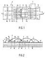
- Fig. 1 shows a known semiconductor device in plan view and Fig. 2 in cross-section taken on the line a-a', provided with an insulating substrate 1 of Al 2 O 3 with a conductive mounting surface 2 on which a bipolar transistor 3 is provided with its first main surface 4 in contact with the mounting surface 2.
- the conductive mounting surface is made of copper.
- the transistor 3 is provided with connection pads 5, 6, 4 for an emitter, base, and collector. These connection pads in the known semiconductor device are connected to further components through bonding wires E1, E2, B1, B2, and C.
- Fig. 1 shows a known semiconductor device in plan view and Fig. 2 in cross-section taken on the line a-a', provided with an insulating substrate 1 of Al 2 O 3 with a conductive mounting surface 2 on which a bipolar transistor 3 is provided with its first main surface 4 in contact with the mounting surface 2.
- the conductive mounting surface is made of copper.
- the transistor 3 is provided with connection pads 5, 6, 4 for an emitter, base, and collector.
- the emitter connection pads 5 are connected to a conductor track 7 via the bonding wires E1 and to a capacitor 8 via the bonding wires E2.
- the capacitor in this example comprises a silicon substrate 9 provided with an insulating layer 10.
- a first electrode 11 of the capacitor 8 is provided on the insulating layer 10. This electrode 11 is connected to the bonding wires B 1 and B2.
- the silicon substrate 9 acts as the second electrode of the capacitor 8.
- the silicon substrate 9 is connected to a conductive mounting surface 12 on which the bonding wire E2 is provided as a so-called zero-ohmic contact.
- the base connection pads 6 are provided in a twofold arrangement and are connected to the electrode 11 of the capacitor 8 via bonding wires B 1 and are further connected to a conductor track 15 via bonding wires B2.
- the collector connection pad 4 is present on the first main surface 4 of the transistor 3.
- the transistor 3 is soldered with its first main surface 4 against the conductive mounting surface 2 by means of a solder layer 16.
- the conductive mounting surface 2 is much larger than the dimensions of the first main surface 4 of the transistor because solder 16 flows out during the application of the transistor 3 on the conductive mounting surface 2, and a portion 16' of the conductive mounting surface 2 lying outside the portion covered by the transistor 3 becomes covered with solder.
- a bonding wire C for the collector cannot be reliably fastened to this portion 16' covered with solder.
- the conductive mounting surface 2 is much larger than the dimensions of the first main surface 4 of the transistor 3 so that a bonding wire for the collector can nevertheless be reliably fastened.
- the bonding wire C in this example is connected through to the conductor track 17.
- An alternative known solution is to provide the conductive mounting surface 2 with a groove for preventing flowing-out of the solder. The solder remains in the groove then and the portion 16' is small or absent.
- the semiconductor device is specially designed for large currents and high operating frequencies, for example above approximately I GHz.
- Several emitter bonding wires E1, E2 provide a low self-inductance of the bonding wires and good high-frequency properties.
- bonding wires C for the collector connection achieves that the transistor performance is not adversely affected by an excessively high resistance in the collector connection at comparatively high currents through the collector.
- the bonding wires are so provided in practice that the bonding wires B1, B2, E1, E2, C run parallel, for reasons of manufacturing technology and also to achieve an optimum space utilization.
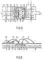
- Figs. 3 and 4 show part of a semiconductor device according to the invention where the connection pads 5 of the emitter, the connection pads 6 of the base, and the connection pads 40 of the collector are situated on a second main surface 12 of the transistor 3 lying opposite the first main surface 4, the dimensions of the conductive mounting surface 2 being substantially equal to the dimensions of the first main surface 4 of the transistor 3.
- the collector connection pad 40 now lies on the second main surface 12 of the transistor 3.
- the conductive mounting surface 2 to which the first main surface 4 of the transistor 3 is applied can be chosen to be comparatively small now. This is because no bonding wires C for connecting the collector are provided on this mounting surface 2. It is sufficient when this mounting surface 2 is so large that the transistor 3 can be easily provided thereon, i.e.
- the dimensions of the conductive mounting surface 2 are approximately equal to the dimensions of the first main surface 4 of the transistor 3.
- the mounting surface 2 may be taken a little larger than the first main surface 4 in view of, for example, alignment tolerances and inaccuracies in the manufacturing process.
- the conductive mounting surface 2 in known semiconductor devices is comparatively large compared with the dimensions of the transistor 3 because bonding wires C are provided on the mounting surface 2.
- the high-frequency properties of the transistor 3 are strongly dependent on the size of the conductive mounting surface 2.
- the conductive mounting surface 2 in combination with the insulating substrate 1 in fact forms a parasitic capacitance with the conductive ground surface 18 on which the insulating substrate 1 is mounted, in this example a heat sink for draining off heat generated in transistor 3.
- the bonding wires E1 for the emitter connection pads may also be made shorter because these wires no longer have to be passed over a comparatively large conductive mounting surface 2.
- the shorter emitter bonding wires provide a lower self-inductance in the emitter bonding wires, and accordingly better high-frequency properties.
- the materials, the connections of the bonding wires, the capacitor 8, and the conductor tracks are identical to those in the known embodiment shown in Figs. 1 and 2 in all other respects.
- the substrate 1 is provided with a cavity 20 at the area of the conductive mounting surface 2, in which cavity a body 21 with a thermal conductivity of more than 10 W/mK is present, a so-called insert.
- the transistor 3 is fixed on the body 21 by means of a solder layer 16.
- the solder layer 16 in this example at the same time constitutes the conductive mounting surface 2.
- the dimensions of the body 21 correspond to those of the conductive mounting surface 2.
- the body 21 is provided so as to achieve a better heat removal than in the first embodiment shown in Figs. 3 and 4 without a body 21.
- the body 16 is made of BeO in this example. BeO has a thermal conductivity of approximately 250 W/mK. Alternatively, the body may be made from AIN or BN.
- the high-frequency transistor 3 comprises a semiconductor substrate in which base, emitter, and collector regions are provided in a manner known in IC technology. These regions are provided, for example, in the form of fingers. More details on such a transistor can be found in European Patent Application 96201822.2.
- connection pads and bonding wires are used for the base, emitter, and collector in the examples. It will be obvious that other numbers of connection pads, such as single pads or indeed larger numbers of connection pads, are possible. It is also possible to make connection pads so large that several bonding wires can be applied to one pad.
- the transistor 3 in this example is connected by its emitter and base to capacitors. Other configurations are also possible.
- the base, emitter, and collector may thus be connected to resistors, capacitors, inputs or outputs of semiconductor devices such as diodes, transistors. or ICs.
- the substrate in the embodiments is made from Al 2 O 3 , but it is alternatively possible to manufacture the substrate from other insulating materials such as, for example, AIN.
Landscapes
- Bipolar Transistors (AREA)
- Wire Bonding (AREA)
Claims (6)
- Halbleiteranordnung, welche mit einem Isolatorsubstrat (1) und einer leitenden Montagefläche (2) versehen ist, wobei das Isolatorsubstrat (1) auf einer leitenden Bodenfläche (18) vorgesehen, ein Bipolartransistor (3) auf der Montagefläche (2) angeordnet, eine erste Hauptoberfläche (4) des Transistors (3) an die Montagefläche (2) gelötet und der Transistor (3) mit Anschlussstellen (5,6,40) eines Emitters, einer Basis und eines Kollektors versehen ist, dadurch gekennzeichnet, dass die Anschlussstellen (5,6,40) des Emitters, der Basis und des Kollektors auf einer, der ersten Hauptoberfläche (4) gegenüberliegenden, zweiten Hauptoberfläche (12) vorgesehen sind, und dass die lateralen Dimensionen der leitenden Montagefläche (2) im Wesentlichen den Dimensionen der ersten Hauptoberfläche (4) des Transistors (3) entsprechen.
- Halbleiteranordnung nach Anspruch 1, dadurch gekennzeichnet, dass die Anschlussstellen (5,40) des Emitters und Kollektors jeweils über mehrere Bonddrähte (E1,E2,C) mit weiteren Bauelementen der Anordnung verbunden sind.
- Halbleiteranordnung nach Anspruch 1 oder 2, dadurch gekennzeichnet, dass ein Kondensator (8) direkt neben dem Transistor (3) vorgesehen ist, wobei der Kondensator (8) ein Siliciumsubstrat (9) mit einer Isolationsschicht (10) aufweist, eine erste Elektrode (11) mit Bonddrähten (B1,B2) der Basis und eine leitende Montagefläche (12) mit Bonddrähten (E2) des Emitters verbunden ist, wobei das Siliciumsubstrat (9) als zweite Elektrode wirkt.
- Halbleiteranordnung nach Anspruch 1, dadurch gekennzeichnet, dass das Substrat (1) mit einem Aufnahmeraum (20) versehen ist, welcher sich bis hinunter zu der Bodenfläche (18) ausdehnt, wobei in dem Aufnahmeraum ein isolierter Körper (21) vorgesehen ist und durch eine erste Seite einen Kontakt mit der Bodenfläche (18) herstellt, während eine zweite Seite des Körpers (21), welche sich gegenüber der ersten Seite befindet, mit der Montagefläche (2) versehen ist, auf welcher der Transistor (3) angeordnet wird, wobei der Körper (21) ein Material mit einer Wärmeleitfähigkeit von mehr als 10 W/mk enthält.
- Halbleiteranordnung nach Anspruch 4, dadurch gekennzeichnet, dass die lateralen Dimensionen des Körpers (21) im Wesentlichen den Dimensionen der Montagefläche (2) entsprechen, wobei die lateralen Dimensionen des Aufnahmeraums (20) so bemessen sind, dass der Körper (21) genau in diesen passt.
- Halbleiteranordnung nach Anspruch 4 oder 5, dadurch gekennzeichnet, dass eine Dicke des Körpers (21) senkrecht zu seinen lateralen Dimensionen geringer als die Dicke des Isolatorsubstrats (1) ist.
Priority Applications (1)
| Application Number | Priority Date | Filing Date | Title |
|---|---|---|---|
| EP97940306A EP0878025B1 (de) | 1996-11-05 | 1997-10-02 | Halbleitervorrichtung mit hochfrequenz-bipolar-transistor auf einem isolierenden substrat |
Applications Claiming Priority (4)
| Application Number | Priority Date | Filing Date | Title |
|---|---|---|---|
| EP96203079 | 1996-11-05 | ||
| EP96203079 | 1996-11-05 | ||
| EP97940306A EP0878025B1 (de) | 1996-11-05 | 1997-10-02 | Halbleitervorrichtung mit hochfrequenz-bipolar-transistor auf einem isolierenden substrat |
| PCT/IB1997/001194 WO1998020553A1 (en) | 1996-11-05 | 1997-10-02 | Semiconductor device with a high-frequency bipolar transistor on an insulating substrate |
Publications (2)
| Publication Number | Publication Date |
|---|---|
| EP0878025A1 EP0878025A1 (de) | 1998-11-18 |
| EP0878025B1 true EP0878025B1 (de) | 2004-04-14 |
Family
ID=8224552
Family Applications (1)
| Application Number | Title | Priority Date | Filing Date |
|---|---|---|---|
| EP97940306A Expired - Lifetime EP0878025B1 (de) | 1996-11-05 | 1997-10-02 | Halbleitervorrichtung mit hochfrequenz-bipolar-transistor auf einem isolierenden substrat |
Country Status (6)
| Country | Link |
|---|---|
| US (1) | US6087721A (de) |
| EP (1) | EP0878025B1 (de) |
| JP (1) | JP4215133B2 (de) |
| KR (1) | KR100503531B1 (de) |
| DE (1) | DE69728648T2 (de) |
| WO (1) | WO1998020553A1 (de) |
Families Citing this family (13)
| Publication number | Priority date | Publication date | Assignee | Title |
|---|---|---|---|---|
| AU705177B1 (en) * | 1997-11-26 | 1999-05-20 | Kabushiki Kaisha Toshiba | Semiconductor device |
| US6259157B1 (en) * | 1998-03-11 | 2001-07-10 | Sanyo Electric Co., Ltd. | Hybrid integrated circuit device, and method of manufacturing thereof |
| US6529081B1 (en) | 2000-06-08 | 2003-03-04 | Zeta, Division Of Sierra Tech Inc. | Method of operating a solid state power amplifying device |
| WO2002005342A1 (en) * | 2000-07-06 | 2002-01-17 | Zeta, A Division Of Sierratech, Inc. | A solid state power amplifying device |
| ATE417361T1 (de) * | 2001-01-18 | 2008-12-15 | Nxp Bv | Leistungstransistor mit intern kombinierten tiefpass- und bandpass-anpassungsstufen |
| CN100459116C (zh) * | 2002-04-11 | 2009-02-04 | 皇家飞利浦电子股份有限公司 | 电子器件及其制造方法 |
| JP3896029B2 (ja) * | 2002-04-24 | 2007-03-22 | 三洋電機株式会社 | 混成集積回路装置の製造方法 |
| US7173328B2 (en) * | 2004-04-06 | 2007-02-06 | Lsi Logic Corporation | Integrated circuit package and method having wire-bonded intra-die electrical connections |
| KR100878708B1 (ko) * | 2007-09-04 | 2009-01-14 | 알.에프 에이치아이씨 주식회사 | 고출력 반도체 소자 패키지 및 방법 |
| DE102010001788A1 (de) | 2010-02-10 | 2011-08-11 | Forschungsverbund Berlin e.V., 12489 | Skalierbarer Aufbau für laterale Halbleiterbauelemente mit hoher Stromtragfähigkeit |
| CN114521290B (zh) * | 2019-09-27 | 2025-09-02 | 株式会社村田制作所 | 电子模块 |
| JP7631157B2 (ja) * | 2021-09-17 | 2025-02-18 | 株式会社東芝 | 半導体装置 |
| KR102730756B1 (ko) * | 2024-04-03 | 2024-11-18 | 주식회사 웨이비스 | 반도체 소자 |
Family Cites Families (12)
| Publication number | Priority date | Publication date | Assignee | Title |
|---|---|---|---|---|
| US3784884A (en) * | 1972-11-03 | 1974-01-08 | Motorola Inc | Low parasitic microwave package |
| NL8202470A (nl) * | 1982-06-18 | 1984-01-16 | Philips Nv | Hoogfrequentschakelinrichting en halfgeleiderinrichting voor toepassing in een dergelijke inrichting. |
| JPH0767055B2 (ja) * | 1989-12-05 | 1995-07-19 | 三菱電機株式会社 | 高周波半導体装置 |
| US5198904A (en) * | 1991-02-25 | 1993-03-30 | Comark Communications, Inc. | Aural carrier correction system and method |
| JP2728322B2 (ja) * | 1991-09-05 | 1998-03-18 | 三菱電機株式会社 | 半導体装置 |
| JPH0595212A (ja) * | 1991-10-01 | 1993-04-16 | Mitsubishi Electric Corp | 高周波半導体混成集積回路装置 |
| US5151775A (en) * | 1991-10-07 | 1992-09-29 | Tektronix, Inc. | Integrated circuit device having improved substrate capacitance isolation |
| EP0590804B1 (de) * | 1992-09-03 | 1997-02-05 | STMicroelectronics, Inc. | Vertikal isolierter, monolithischer Hochleistungsbipolartransistor mit Topkollektor |
| JPH06260563A (ja) * | 1993-03-03 | 1994-09-16 | Mitsubishi Electric Corp | トランジスタ用パッケージ |
| US5397917A (en) * | 1993-04-26 | 1995-03-14 | Motorola, Inc. | Semiconductor package capable of spreading heat |
| JP3987573B2 (ja) * | 1994-10-31 | 2007-10-10 | コーニンクレッカ フィリップス エレクトロニクス エヌ ヴィ | 能動素子及び受動素子を有する集積化された半導体装置 |
| US5986324A (en) * | 1997-04-11 | 1999-11-16 | Raytheon Company | Heterojunction bipolar transistor |
-
1997
- 1997-10-02 WO PCT/IB1997/001194 patent/WO1998020553A1/en not_active Ceased
- 1997-10-02 EP EP97940306A patent/EP0878025B1/de not_active Expired - Lifetime
- 1997-10-02 JP JP52116098A patent/JP4215133B2/ja not_active Expired - Lifetime
- 1997-10-02 KR KR10-1998-0705131A patent/KR100503531B1/ko not_active Expired - Fee Related
- 1997-10-02 DE DE69728648T patent/DE69728648T2/de not_active Expired - Lifetime
- 1997-11-03 US US08/963,647 patent/US6087721A/en not_active Expired - Lifetime
Also Published As
| Publication number | Publication date |
|---|---|
| EP0878025A1 (de) | 1998-11-18 |
| KR19990077001A (ko) | 1999-10-25 |
| WO1998020553A1 (en) | 1998-05-14 |
| KR100503531B1 (ko) | 2005-09-26 |
| DE69728648T2 (de) | 2005-03-31 |
| JP4215133B2 (ja) | 2009-01-28 |
| JP2000504490A (ja) | 2000-04-11 |
| US6087721A (en) | 2000-07-11 |
| DE69728648D1 (de) | 2004-05-19 |
Similar Documents
| Publication | Publication Date | Title |
|---|---|---|
| US4918571A (en) | Chip carrier with energy storage means | |
| KR100412056B1 (ko) | 마이크로웨이브하이브리드집적회로 | |
| US5075759A (en) | Surface mounting semiconductor device and method | |
| JP3051011B2 (ja) | パワ−モジュ−ル | |
| EP1143514A2 (de) | Kunststoffeingekapselte Leistungshalbleiteranordnung einschliesslich einem Substrat mit allen darauf montierten elektronischen Bauteilen für eine Kontrollschaltung | |
| US5130768A (en) | Compact, high-density packaging apparatus for high performance semiconductor devices | |
| KR20010071766A (ko) | 반도체 소자용 캡슐 | |
| EP0878025B1 (de) | Halbleitervorrichtung mit hochfrequenz-bipolar-transistor auf einem isolierenden substrat | |
| JPH033290A (ja) | 電子回路アセンブリ用サーマルシヤント及びその製造方法 | |
| JP3943165B2 (ja) | チップ・スタックおよびコンデンサ取付の配置 | |
| KR100419428B1 (ko) | 고전력마이크로파하이브리드집적회로 | |
| US5889319A (en) | RF power package with a dual ground | |
| EP0253295A1 (de) | Thermisch verbessertes Gehäuse für eine LSI-integrierte Schaltung | |
| KR100771262B1 (ko) | 고전력 애플리케이션에 사용하기 위한 다중칩 모듈 | |
| JPH08274228A (ja) | 半導体搭載基板、電力用半導体装置及び電子回路装置 | |
| EP0408904A2 (de) | Oberflächenmontierbare Halbleitervorrichtung und Verfahren | |
| US11879790B2 (en) | Isolated temperature sensor package with embedded spacer in dielectric opening | |
| JP2919674B2 (ja) | 混成集積回路 | |
| CN100401510C (zh) | 半导体装置、半导体主体及其制造方法 | |
| EP0285277A1 (de) | Chipträger mit Mitteln für Energiespeicherung | |
| KR940008342B1 (ko) | 필름캐리어를 이용한 반도체장치 | |
| JP2583507B2 (ja) | 半導体実装回路装置 | |
| JPH0464467B2 (de) | ||
| JPH0714938A (ja) | 混成集積回路装置 | |
| JPH05109940A (ja) | 混成集積回路 |
Legal Events
| Date | Code | Title | Description |
|---|---|---|---|
| PUAI | Public reference made under article 153(3) epc to a published international application that has entered the european phase |
Free format text: ORIGINAL CODE: 0009012 |
|
| AK | Designated contracting states |
Kind code of ref document: A1 Designated state(s): DE FR GB NL |
|
| 17P | Request for examination filed |
Effective date: 19981116 |
|
| 17Q | First examination report despatched |
Effective date: 20020215 |
|
| GRAP | Despatch of communication of intention to grant a patent |
Free format text: ORIGINAL CODE: EPIDOSNIGR1 |
|
| GRAS | Grant fee paid |
Free format text: ORIGINAL CODE: EPIDOSNIGR3 |
|
| GRAA | (expected) grant |
Free format text: ORIGINAL CODE: 0009210 |
|
| AK | Designated contracting states |
Kind code of ref document: B1 Designated state(s): DE FR GB NL |
|
| PG25 | Lapsed in a contracting state [announced via postgrant information from national office to epo] |
Ref country code: NL Free format text: LAPSE BECAUSE OF FAILURE TO SUBMIT A TRANSLATION OF THE DESCRIPTION OR TO PAY THE FEE WITHIN THE PRESCRIBED TIME-LIMIT Effective date: 20040414 |
|
| REG | Reference to a national code |
Ref country code: GB Ref legal event code: FG4D |
|
| REF | Corresponds to: |
Ref document number: 69728648 Country of ref document: DE Date of ref document: 20040519 Kind code of ref document: P |
|
| NLV1 | Nl: lapsed or annulled due to failure to fulfill the requirements of art. 29p and 29m of the patents act | ||
| ET | Fr: translation filed | ||
| PLBE | No opposition filed within time limit |
Free format text: ORIGINAL CODE: 0009261 |
|
| STAA | Information on the status of an ep patent application or granted ep patent |
Free format text: STATUS: NO OPPOSITION FILED WITHIN TIME LIMIT |
|
| 26N | No opposition filed |
Effective date: 20050117 |
|
| REG | Reference to a national code |
Ref country code: GB Ref legal event code: 732E |
|
| REG | Reference to a national code |
Ref country code: FR Ref legal event code: TP |
|
| REG | Reference to a national code |
Ref country code: GB Ref legal event code: 732E Free format text: REGISTERED BETWEEN 20121108 AND 20121114 |
|
| REG | Reference to a national code |
Ref country code: DE Ref legal event code: R082 Ref document number: 69728648 Country of ref document: DE Representative=s name: MUELLER-BORE & PARTNER PATENTANWAELTE, EUROPEA, DE |
|
| REG | Reference to a national code |
Ref country code: DE Ref legal event code: R082 Ref document number: 69728648 Country of ref document: DE Representative=s name: MUELLER-BORE & PARTNER PATENTANWAELTE PARTG MB, DE Effective date: 20130211 Ref country code: DE Ref legal event code: R082 Ref document number: 69728648 Country of ref document: DE Representative=s name: MUELLER-BORE & PARTNER PATENTANWAELTE, EUROPEA, DE Effective date: 20130211 Ref country code: DE Ref legal event code: R081 Ref document number: 69728648 Country of ref document: DE Owner name: CALLAHAN CELLULAR L.L.C., WILMINGTON, US Free format text: FORMER OWNER: NXP B.V., EINDHOVEN, NL Effective date: 20130211 Ref country code: DE Ref legal event code: R081 Ref document number: 69728648 Country of ref document: DE Owner name: CALLAHAN CELLULAR L.L.C., US Free format text: FORMER OWNER: NXP B.V., EINDHOVEN, NL Effective date: 20130211 |
|
| REG | Reference to a national code |
Ref country code: FR Ref legal event code: TP Owner name: CALLAHAN CELLULAR L.L.C., US Effective date: 20130724 |
|
| REG | Reference to a national code |
Ref country code: FR Ref legal event code: PLFP Year of fee payment: 20 |
|
| PGFP | Annual fee paid to national office [announced via postgrant information from national office to epo] |
Ref country code: GB Payment date: 20160926 Year of fee payment: 20 |
|
| PGFP | Annual fee paid to national office [announced via postgrant information from national office to epo] |
Ref country code: FR Payment date: 20160926 Year of fee payment: 20 |
|
| PGFP | Annual fee paid to national office [announced via postgrant information from national office to epo] |
Ref country code: DE Payment date: 20161031 Year of fee payment: 20 |
|
| REG | Reference to a national code |
Ref country code: DE Ref legal event code: R071 Ref document number: 69728648 Country of ref document: DE |
|
| REG | Reference to a national code |
Ref country code: GB Ref legal event code: PE20 Expiry date: 20171001 |
|
| PG25 | Lapsed in a contracting state [announced via postgrant information from national office to epo] |
Ref country code: GB Free format text: LAPSE BECAUSE OF EXPIRATION OF PROTECTION Effective date: 20171001 |