EP0893882A2 - Hochfrequenzschaltungsanordnung, Eingabeeinheit und Transceiver - Google Patents
Hochfrequenzschaltungsanordnung, Eingabeeinheit und Transceiver Download PDFInfo
- Publication number
- EP0893882A2 EP0893882A2 EP98305931A EP98305931A EP0893882A2 EP 0893882 A2 EP0893882 A2 EP 0893882A2 EP 98305931 A EP98305931 A EP 98305931A EP 98305931 A EP98305931 A EP 98305931A EP 0893882 A2 EP0893882 A2 EP 0893882A2
- Authority
- EP
- European Patent Office
- Prior art keywords
- fet
- circuit
- switch device
- inductor
- high frequency
- Prior art date
- Legal status (The legal status is an assumption and is not a legal conclusion. Google has not performed a legal analysis and makes no representation as to the accuracy of the status listed.)
- Granted
Links
Images


Classifications
-
- H—ELECTRICITY
- H03—ELECTRONIC CIRCUITRY
- H03K—PULSE TECHNIQUE
- H03K17/00—Electronic switching or gating, i.e. not by contact-making and –breaking
- H03K17/51—Electronic switching or gating, i.e. not by contact-making and –breaking characterised by the components used
- H03K17/56—Electronic switching or gating, i.e. not by contact-making and –breaking characterised by the components used by the use, as active elements, of semiconductor devices
- H03K17/687—Electronic switching or gating, i.e. not by contact-making and –breaking characterised by the components used by the use, as active elements, of semiconductor devices the devices being field-effect transistors
- H03K17/693—Switching arrangements with several input- or output-terminals, e.g. multiplexers, distributors
-
- H—ELECTRICITY
- H03—ELECTRONIC CIRCUITRY
- H03K—PULSE TECHNIQUE
- H03K17/00—Electronic switching or gating, i.e. not by contact-making and –breaking
- H03K17/06—Modifications for ensuring a fully conducting state
- H03K17/063—Modifications for ensuring a fully conducting state in field-effect transistor switches
-
- H—ELECTRICITY
- H04—ELECTRIC COMMUNICATION TECHNIQUE
- H04B—TRANSMISSION
- H04B1/00—Details of transmission systems, not covered by a single one of groups H04B3/00 - H04B13/00; Details of transmission systems not characterised by the medium used for transmission
- H04B1/38—Transceivers, i.e. devices in which transmitter and receiver form a structural unit and in which at least one part is used for functions of transmitting and receiving
- H04B1/40—Circuits
- H04B1/44—Transmit/receive switching
- H04B1/48—Transmit/receive switching in circuits for connecting transmitter and receiver to a common transmission path, e.g. by energy of transmitter
-
- H—ELECTRICITY
- H03—ELECTRONIC CIRCUITRY
- H03K—PULSE TECHNIQUE
- H03K17/00—Electronic switching or gating, i.e. not by contact-making and –breaking
- H03K17/06—Modifications for ensuring a fully conducting state
- H03K2017/066—Maximizing the OFF-resistance instead of minimizing the ON-resistance
-
- H—ELECTRICITY
- H03—ELECTRONIC CIRCUITRY
- H03K—PULSE TECHNIQUE
- H03K2217/00—Indexing scheme related to electronic switching or gating, i.e. not by contact-making or -breaking covered by H03K17/00
- H03K2217/0054—Gating switches, e.g. pass gates
-
- H—ELECTRICITY
- H03—ELECTRONIC CIRCUITRY
- H03K—PULSE TECHNIQUE
- H03K2217/00—Indexing scheme related to electronic switching or gating, i.e. not by contact-making or -breaking covered by H03K17/00
- H03K2217/009—Resonant driver circuits
Definitions
- the present invention relates to a high frequency switch device, front end unit and transceiver, and more specifically to a high frequency switch device, front end unit and transceiver, for switching an input path of RF (radio frequency) signals to an output path thereof or vice versa in transmission or reception mode of an RF transmitter/receiver.
- RF radio frequency
- a single pole dual through (SPDT) switch device composed of four FETs 11, 12, 13 and 14, as shown in Fig. 10, has been widely adopted as a high frequency switch device used for a mobile communication system.
- a signal input/output terminal 2 is used as an antenna terminal;
- a signal input/output terminal 3 is used as a transmit-side terminal Tx of a transmit-side power transmission path;
- a signal input/output terminal 4 is used as a receive-side terminal Rx of a receive-side small-signal transmission path, under consideration of a switch for switching an antenna of a digital cordless telephone from transmission state to reception state or vice versa.
- the various losses are an on-resistance loss of the FET 11, a leakage loss through a source-drain capacitance C off obtained when the FET 13 is turned off, and a leakage loss through a source-drain capacitance C off obtained when the off-side FET 12 is turned off.
- a parallel-resonance type switch device as shown in Fig. 8 has been proposed, which was already filed in Japanese Patent Office by the same Applicant (Japanese Published Unexamined Patent Application No. 9-23101).
- this switch device without providing the FETs 13 and 14 connected in parallel to the respective transmission path as with the case of the prior art SPDT switch device shown in Fig. 10, each of two inductors 21 and 22 is connected between the source electrode and the drain electrode of each of the FETs 11 and 12, respectively in such a way that a resonance circuit can be formed in cooperation with each of the off-state capacitances C off of both the FETs 11 and 12.
- a voltage supply terminal 6 for setting a reference voltage is connected to a junction point 8 of both the FETs 11 and 12 via a high resistance element 32, and further a control signal is applied to each of the gates of the FETs 11 and 12 via each of high resistance elements 31 and 33, respectively.
- the switch device is manufactured by a MMIC (Microwave Monolithic Integrated Circuit)
- MMIC Microwave Monolithic Integrated Circuit
- Fig. 9 shows a layout pattern of the high frequency switch device shown in Fig. 8, in which a transmit-side terminal 3 of the transmit-side power transmission path is formed on the right side; and the receive-side terminal 4 of the receive-side small-signal transmission path is formed on the left side; the antenna terminal 2 is formed on the middle lower side; and the two gate signal input terminals 5 and 7 and the supply voltage terminal 6 are all formed on the middle upper side.
- the inductance 21 or 22 is a spiral inductor of 360 ⁇ m-square, in which each line width is designed as 10 ⁇ m and each space therebetween is designed as 5 ⁇ m. Further, the total chip area is 0.9mm x0.9mm.
- the second higher harmonic spurious signal In the PHS specifications decided by the RCR standard, the second higher harmonic spurious signal must be less than -45dBc when the output power is 19dBm. In the case of the resonance type high frequency switch device shown in Fig. 8, since the second higher harmonic spurious signal is -42dBc, it is impossible to satisfy the RCR standard.
- the present invention provides a high frequency switch device, comprising: first, second and third terminals; a first circuit composed of a first FET, and a first inductor and a first capacitor both connected with said first FET in parallel to each other, one end of said first circuit being connected to said first terminal; and a second circuit composed of a second FET, and a second inductor and a second capacitor both connected with the second FET in parallel to each other, one end of said second circuit being connected to said first circuit and the other end of said second circuit being connected to said second terminal, and wherein a first control signal is applied to a gate of the first FET via a resistance; a second control signal is applied to a gate of the second FET via a resistance; said third terminal (6) is connected to a common junction point of said first and second circuits; and a predetermined potential is applied to the common junction point.
- the high frequency switch device is used to switch radio signal paths when radio signals are given from a transmitter to an antenna or when radio signals are given from the antenna to a receiver; said first and second terminals are connected to the receiver and the transmitter, respectively; and said third terminal is connected to the antenna.
- the first and second capacitors are of linear element, respectively.
- the first and second capacitors are of parallel plane capacitance, respectively.
- the first inductor, a non-linear capacitance obtained when the first FET is turned off, and the first capacitor form a parallel resonance circuit
- the second inductor, another non-linear capacitance obtained when the second FET is turned off, and the second capacitor form another parallel resonance circuit
- the first and second inductors are both so determined as to satisfy a predetermined parallel resonance condition at a predetermined frequency, respectively.
- the high frequency switch device is constructed on a single substrate as one chip; and the first and second capacitors are of metal-insulator-metal structure.
- the first FET is arranged between the first inductor and the first capacitor on a device chip; and the second FET is arranged between the second inductor and the second capacitor on the same device chip.
- the present invention provides a front end unit used at a radio frequency stage of a transceiver and having the same high frequency switch device as defined above.
- the present invention provides a transceiver having the same high frequency switch device as defined above.
- Fig. 1 shows a simple portable telephone system called PHS (Personal Handy-phone System), to which the RF switch device according to the present invention is applied.
- PHS Personal Handy-phone System
- the RF switch device transmits signals received by an antenna to a low noise amplifier in reception mode, but transmits signals amplified by a power amplifier to the antenna in transmission mode, as understood with reference to Fig. 1.
- Fig. 2 shows one embodiment of the high frequency switch device according to the present invention, which is used as an antenna switch for a digital cordless telephone.
- the switch device comprises a first filter circuit composed of a depletion type FET 11, an inductor 21 and a capacitor 25; a second filter circuit composed of a depletion type FET 12, an inductor 22 and a capacitor 26; and three resistors 31, 32 and 33.
- One end of the first filter and one end of the second filter circuits are connected in series with each other, and an antenna terminal (Ant) 2 is connected to a common junction point 8 of the two filter circuits.
- a transmit-side terminal (Tx) 3 is connected to the other end of the first filter circuit
- a receive-side terminal (Rx) 4 is connected to the other end of the second filter circuit.
- a gate signal input terminal 5 is connected to a gate of the FET 11 via the gate resistor 31 of high resistance value (e.g., several k ⁇ ), and a gate signal input terminal 7 is connected to a gate of the FET 12 via the gate resistor 33 of high resistance value (e.g., several k ⁇ ). Further, a reference potential input terminal 6 is connected to the common junction point 8 via the resistor 32 of high resistance value (e.g., several k ⁇ ).
- the inductor 21 and the capacitor 25 are connected in parallel to each other between a drain electrode and a source electrode of the FET 11.
- the inductor 22 and the capacitor 26 are connected in parallel to each other between a drain electrode and a source electrode of the FET 12.
- the inductor 21 forms a parallel resonance circuit in cooperation with both an off-state capacitance of the FET 11 and the capacitor 25. Further, the inductance of the inductor 21 is so decided that the impedance of the parallel resonance circuit can be maximized at a frequency (e.g., 1.9GHz) which is used by the digital cordless telephone.
- the inductor 22 forms a parallel resonance circuit in cooperation with both an off-state capacitance of the FET 12 and the capacitor 26. Further, the inductance of the inductor 22 is so decided that the impedance of the parallel resonance circuit can be maximized at the frequency (e.g., 1.9GHz).
- the inductance value is determined in such a way that the resonance frequency of the parallel resonance circuit is 1.9GHz (the frequency used by the digital cordless telephone).
- the capacitance C rx is the total resonance capacitance obtained when the receive-side or the transmit-side is turned off, which is an addition of the capacitance C p of the capacitor 25 or 26 and the off-state capacitance C off obtained when the FET 11 or FET 12 is turned off.
- the above table indicates that the inductance can be determined small in comparison with that of the prior art case. This is because since the resonance frequency f o can be decided roughly as (C rx . L) -1/2 , when the capacitance C p is added to the off-state capacitance C off as with the case of the present embodiment, it is possible to set the inductance L to a smaller value.
- C p is 0.8pF (in the second example)
- it is possible to reduce the inductance L of the inductor 21 or 22 of the present embodiment less than 1/3 ( 6.0/21.5) of the inductance L of the prior art.
- Fig. 3 shows a layout pattern of the high frequency switch device according to the present invention, in which the reference numerals correspond to those shown in Fig. 2.
- C p is 0.8pF
- the inductor 21 or 22 is a 240 ⁇ m-square spiral inductor so designed that each line width is 10 ⁇ m and each space between the lines is 5 ⁇ m.
- the capacitors 25 and 26 are arranged at opposing positions to the inductors 21 and 22, respectively. Further, the two FETs 11 and 12 are arranged between the two inductors 21 and 22 and the two capacitors 25 and 26, respectively.
- the capacitances 25 and 26 are added in comparison with the prior art switch device, since the areas occupied by the inductors 21 and 22 can be reduced markedly, as compared with that of the prior art switch device, it is possible to reduce the total chip area.
- the chip size of this embodiment is 0.75mmx0.75mm; on the other hand, the chip size of the prior art is 0.9mmx0.9mm.
- elements as shown in Fig. 2 are formed on a GaAs substrate.
- the transmit-side terminal 3 is shown, and a common junction point 8 is shown on the left side of the common junction point 8.
- the transmit-side terminal 3 is connected to the common junction point 8 via the inductor 21 and the capacitor 25 both connected in parallel to the FET 11, respectively.
- the inductor 21 is formed on a substrate Sub in square vortex shape.
- the capacitance 25 is of MIM (metal-insulator-metal) structure.
- the gate signal input terminal 5 is connected to the gate of the FET 11 via the resistance (wire) 31.
- the inductor 22, the capacitor 26, the FET 12, and the receive-side terminal 4 are all formed in the same way as with the case of the above-mentioned right-side structure.
- the capacitances 25 and 26 are of MIM structure, it is possible to realize low-distortion characteristics in switching operation.
- the capacitor to be connected in parallel to the inductor since a capacitor of linear characteristics are preferable, the MIM capacitor is more suitable, as compared with the chip capacitor. This is because in the case of the MIM capacitor, since an element including a smaller parasitic capacitance can be realized, it is possible to obtain a linear operation of the resonance circuit.
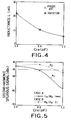
- Fig. 5 shows the relationship between the total resonance capacitance C rx and the second harmonic spurious signal transmitted from the antenna terminal 2 when the transmit input power is 20dBm.
- the solid line denotes the case A in which the capacitance C p of 0pF, 0.4pF or 0.8pF is added to the FET having a gate width W g of 1mm as described above, and the dashed line denotes the case B in which the gate width W g is changed from 1mm to 3mm (from 0.4pF to 1.2pF), without connecting any additional capacitance C p .
- the total resonance capacitor C rx of the case A is composed of a capacitor C p (linear element) and the off-state capacitance C off (non-linear element) of the FET, but the total resonance capacitor C rx of the case B is only an off-state capacitance (non-linear element) of the FET.
- C rx 0.8pF
- the second higher spurious signal of the case A is as small as -46dBc, in comparison with -42dBc of the case B.
- the resonance capacitor includes the capacitance C p (linear element)
- the non-linear characteristics of the leak path in the transmission mode can be reduced and thereby the distortion can be reduced, in comparison with when the resonance capacitor is composed of only the off-state capacitance C off (non-linear element) of the FET.
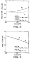
- Fig. 6 shows the relationship between the insertion loss and the total resonance capacitance C rx
- Fig. 7 shows the relationship between the isolation dB and the total resonance capacitance C rx .
- the on-resistance of the FET of the case B is small, as compared with the case A.
- the layout area of the case B is larger than that of the case A. In the actual design, it is desirable to select the value of the capacitance C p under the consideration of the target specifications.
- the capacitors are arranged at opposing positions to the inductors, by arranging the FETs between the capacitors and the inductors, in order to suppress the interference between the elements, the present invention is not limited only to this element arrangement.
- the inductor and the capacitor are connected in parallel to each other between the drain and source electrodes of each FET; since a parallel resonance circuit is formed by use of an inductor and a capacitor in addition to an off-state capacitance of the FET; and further since the inductance is so designed that the impedance of the resonance circuit can be maximized at 1.9GHz used by a digital cordless telephone, the resonance capacitance can be increased and thereby the inductance can be reduced to that extent, with the result that the chip area can be reduced markedly.
- the resonance capacitance is composed of the linear capacitance (of the added capacitor) and the non-linear capacitance (of the off-state capacitance of the FET), it is possible to reduce the non-linear characteristics of the leak path in the transmission mode, so that the signal distortion can be reduced in the transmission mode.
Landscapes
- Engineering & Computer Science (AREA)
- Computer Networks & Wireless Communication (AREA)
- Signal Processing (AREA)
- Electronic Switches (AREA)
- Waveguide Switches, Polarizers, And Phase Shifters (AREA)
- Transceivers (AREA)
Applications Claiming Priority (3)
| Application Number | Priority Date | Filing Date | Title |
|---|---|---|---|
| JP20044697 | 1997-07-25 | ||
| JP200446/97 | 1997-07-25 | ||
| JP20044697A JP3310203B2 (ja) | 1997-07-25 | 1997-07-25 | 高周波スイッチ装置 |
Publications (3)
| Publication Number | Publication Date |
|---|---|
| EP0893882A2 true EP0893882A2 (de) | 1999-01-27 |
| EP0893882A3 EP0893882A3 (de) | 2001-02-14 |
| EP0893882B1 EP0893882B1 (de) | 2003-09-10 |
Family
ID=16424444
Family Applications (1)
| Application Number | Title | Priority Date | Filing Date |
|---|---|---|---|
| EP98305931A Expired - Lifetime EP0893882B1 (de) | 1997-07-25 | 1998-07-24 | Hochfrequenzschaltungsanordnung, Eingabeeinheit und Transceiver |
Country Status (4)
| Country | Link |
|---|---|
| US (1) | US6118985A (de) |
| EP (1) | EP0893882B1 (de) |
| JP (1) | JP3310203B2 (de) |
| DE (1) | DE69817941T2 (de) |
Cited By (6)
| Publication number | Priority date | Publication date | Assignee | Title |
|---|---|---|---|---|
| EP1289159A3 (de) * | 2001-09-03 | 2004-12-29 | Matsushita Electric Industrial Co., Ltd. | Hochfrequenzschalteinrichtung und mobiles Kommunikationsgerät |
| DE10105942B4 (de) * | 2000-02-22 | 2008-07-17 | Murata Mfg. Co., Ltd., Nagaokakyo | Einpoliger Umschalter und Kommunikationseinheit unter Verwendung desselben |
| FR2969428A1 (fr) * | 2010-12-21 | 2012-06-22 | St Microelectronics Sa | Commutateur electronique et appareil de communication incluant un tel commutateur |
| EP2302738A3 (de) * | 2009-09-28 | 2013-03-27 | Fujitsu Limited | Kommunikationsvorrichtung |
| CN103548265A (zh) * | 2011-06-06 | 2014-01-29 | 住友电气工业株式会社 | 开关电路 |
| CN108574479A (zh) * | 2017-03-08 | 2018-09-25 | 康希通信科技(上海)有限公司 | 单刀单掷射频开关及其构成的单刀多掷射频开关 |
Families Citing this family (52)
| Publication number | Priority date | Publication date | Assignee | Title |
|---|---|---|---|---|
| JP2000114950A (ja) * | 1998-10-07 | 2000-04-21 | Murata Mfg Co Ltd | Spstスイッチおよびspdtスイッチおよびそれを用いた通信機 |
| US6396325B2 (en) * | 1999-12-03 | 2002-05-28 | Fairchild Semiconductor Corporation | High frequency MOSFET switch |
| JP2002050980A (ja) * | 2000-08-04 | 2002-02-15 | Matsushita Electric Ind Co Ltd | 高周波スイッチおよびそれを用いた無線通信機 |
| JP2002135095A (ja) | 2000-10-26 | 2002-05-10 | Nec Kansai Ltd | Icスイッチ |
| JP3469563B2 (ja) * | 2001-05-14 | 2003-11-25 | 三菱電機株式会社 | 移相器及び多ビット移相器 |
| JP2002353411A (ja) * | 2001-05-25 | 2002-12-06 | Sanyo Electric Co Ltd | 化合物半導体スイッチ回路装置 |
| JP2002368194A (ja) * | 2001-06-08 | 2002-12-20 | Sanyo Electric Co Ltd | 化合物半導体スイッチ回路装置 |
| US7369535B2 (en) * | 2001-06-11 | 2008-05-06 | Level 3 Communications, Llc | Voice over Internet Protocol real time protocol routing |
| JP4534405B2 (ja) * | 2001-09-25 | 2010-09-01 | 株式会社村田製作所 | 高周波スイッチ回路およびそれを用いた電子装置 |
| JP3813083B2 (ja) * | 2001-12-05 | 2006-08-23 | ローム株式会社 | 送受信装置 |
| US6774718B2 (en) * | 2002-07-19 | 2004-08-10 | Micro Mobio Inc. | Power amplifier module for wireless communication devices |
| US7493094B2 (en) * | 2005-01-19 | 2009-02-17 | Micro Mobio Corporation | Multi-mode power amplifier module for wireless communication devices |
| US7071783B2 (en) * | 2002-07-19 | 2006-07-04 | Micro Mobio Corporation | Temperature-compensated power sensing circuit for power amplifiers |
| US20040232982A1 (en) * | 2002-07-19 | 2004-11-25 | Ikuroh Ichitsubo | RF front-end module for wireless communication devices |
| US7421389B2 (en) * | 2002-11-13 | 2008-09-02 | At&T Knowledge Ventures, L.P. | System and method for remote speech recognition |
| US7248035B2 (en) * | 2002-12-12 | 2007-07-24 | Analog Devices, Inc. | Automatic test equipment pin channel with T-coil compensation |
| DE10313868B4 (de) * | 2003-03-21 | 2009-11-19 | Siemens Ag | Katheter zur magnetischen Navigation |
| US7468543B2 (en) * | 2003-09-19 | 2008-12-23 | Kabushiki Kaisha Toshiba | Semiconductor device, communication device, and semiconductor device inspecting method |
| US20050205986A1 (en) * | 2004-03-18 | 2005-09-22 | Ikuroh Ichitsubo | Module with integrated active substrate and passive substrate |
| US7254371B2 (en) * | 2004-08-16 | 2007-08-07 | Micro-Mobio, Inc. | Multi-port multi-band RF switch |
| US7389090B1 (en) | 2004-10-25 | 2008-06-17 | Micro Mobio, Inc. | Diplexer circuit for wireless communication devices |
| US7262677B2 (en) * | 2004-10-25 | 2007-08-28 | Micro-Mobio, Inc. | Frequency filtering circuit for wireless communication devices |
| US7391282B2 (en) | 2004-11-17 | 2008-06-24 | Matsushita Electric Industrial Co., Ltd. | Radio-frequency switch circuit and semiconductor device |
| US7221225B2 (en) | 2004-12-03 | 2007-05-22 | Micro-Mobio | Dual band power amplifier module for wireless communication devices |
| US7084702B1 (en) * | 2005-01-19 | 2006-08-01 | Micro Mobio Corp. | Multi-band power amplifier module for wireless communication devices |
| US7548111B2 (en) * | 2005-01-19 | 2009-06-16 | Micro Mobio Corporation | Miniature dual band power amplifier with reserved pins |
| US7769355B2 (en) * | 2005-01-19 | 2010-08-03 | Micro Mobio Corporation | System-in-package wireless communication device comprising prepackaged power amplifier |
| US7580687B2 (en) * | 2005-01-19 | 2009-08-25 | Micro Mobio Corporation | System-in-package wireless communication device comprising prepackaged power amplifier |
| US20070063982A1 (en) * | 2005-09-19 | 2007-03-22 | Tran Bao Q | Integrated rendering of sound and image on a display |
| US7477204B2 (en) * | 2005-12-30 | 2009-01-13 | Micro-Mobio, Inc. | Printed circuit board based smart antenna |
| JP4464368B2 (ja) * | 2006-05-23 | 2010-05-19 | Necエレクトロニクス株式会社 | スイッチ回路 |
| US7477108B2 (en) * | 2006-07-14 | 2009-01-13 | Micro Mobio, Inc. | Thermally distributed integrated power amplifier module |
| DE102006052433A1 (de) * | 2006-11-07 | 2008-05-08 | Rohde & Schwarz Gmbh & Co. Kg | Hochfrequenz-Umschalter |
| JP2009159059A (ja) | 2007-12-25 | 2009-07-16 | Samsung Electro Mech Co Ltd | 高周波スイッチ回路 |
| TWI350053B (en) * | 2008-01-25 | 2011-10-01 | Univ Nat Taiwan | Single-pole single-throw switch circuit device |
| US7852063B2 (en) * | 2008-06-04 | 2010-12-14 | Silicon Storage Technology, Inc. | Integrated power detector with temperature compensation for fully-closed loop control |
| JP5114304B2 (ja) * | 2008-06-13 | 2013-01-09 | 新日本無線株式会社 | 半導体スイッチ集積回路 |
| JP5336232B2 (ja) * | 2009-03-18 | 2013-11-06 | 住友電工デバイス・イノベーション株式会社 | スイッチング回路及びその試験方法 |
| KR101301209B1 (ko) * | 2009-12-16 | 2013-08-29 | 한국전자통신연구원 | 고주파 대역 스위칭용 씨모오스 스위치 및 스위칭 격리도 강화방법 |
| JP5632663B2 (ja) * | 2010-06-29 | 2014-11-26 | ルネサスエレクトロニクス株式会社 | 半導体装置 |
| US8405453B2 (en) * | 2010-07-20 | 2013-03-26 | International Business Machines Corporation | Millimeter-wave on-chip switch employing frequency-dependent inductance for cancellation of off-state capacitance |
| KR20130127782A (ko) * | 2012-05-15 | 2013-11-25 | 삼성전기주식회사 | 스위칭 회로 및 이를 포함하는 무선통신 시스템 |
| US9024838B2 (en) | 2012-08-09 | 2015-05-05 | Qualcomm Incorporated | Multi-throw antenna switch with off-state capacitance reduction |
| US9729190B2 (en) * | 2014-01-17 | 2017-08-08 | Qualcomm Incorporated | Switchable antenna array |
| US9847804B2 (en) | 2014-04-30 | 2017-12-19 | Skyworks Solutions, Inc. | Bypass path loss reduction |
| GB2527638B (en) * | 2014-04-30 | 2019-03-27 | Skyworks Solutions Inc | Bypass path loss reduction |
| US9479160B2 (en) | 2014-12-17 | 2016-10-25 | GlobalFoundries, Inc. | Resonant radio frequency switch |
| JP6832871B2 (ja) * | 2015-12-28 | 2021-02-24 | 株式会社村田製作所 | マルチプレクサ |
| US9735854B2 (en) * | 2016-01-18 | 2017-08-15 | Qorvo Us, Inc. | Systems for antenna swapping switching and methods of operation thereof |
| US9793972B1 (en) | 2016-04-04 | 2017-10-17 | Qorvo Us, Inc. | Multiple-input multiple-output (MIMO) antenna swapping circuit |
| US10594357B2 (en) * | 2017-11-07 | 2020-03-17 | Qorvo Us, Inc. | Radio frequency switch system |
| US10992334B2 (en) | 2019-04-04 | 2021-04-27 | Analog Devices International Unlimited Company | Radio frequency switches with controllable resonant frequency |
Family Cites Families (6)
| Publication number | Priority date | Publication date | Assignee | Title |
|---|---|---|---|---|
| JP3169775B2 (ja) * | 1994-08-29 | 2001-05-28 | 株式会社日立製作所 | 半導体回路、スイッチ及びそれを用いた通信機 |
| JPH08204530A (ja) * | 1995-01-23 | 1996-08-09 | Sony Corp | スイツチ回路 |
| JPH098501A (ja) * | 1995-06-15 | 1997-01-10 | Hitachi Ltd | 高周波スイッチ |
| JPH0923101A (ja) * | 1995-07-05 | 1997-01-21 | Toshiba Corp | 高周波スイッチ装置 |
| JP3249393B2 (ja) * | 1995-09-28 | 2002-01-21 | 株式会社東芝 | スイッチ回路 |
| JPH09200021A (ja) * | 1996-01-22 | 1997-07-31 | Mitsubishi Electric Corp | 集積回路 |
-
1997
- 1997-07-25 JP JP20044697A patent/JP3310203B2/ja not_active Expired - Fee Related
-
1998
- 1998-07-24 EP EP98305931A patent/EP0893882B1/de not_active Expired - Lifetime
- 1998-07-24 US US09/121,939 patent/US6118985A/en not_active Expired - Fee Related
- 1998-07-24 DE DE69817941T patent/DE69817941T2/de not_active Expired - Fee Related
Cited By (9)
| Publication number | Priority date | Publication date | Assignee | Title |
|---|---|---|---|---|
| DE10105942B4 (de) * | 2000-02-22 | 2008-07-17 | Murata Mfg. Co., Ltd., Nagaokakyo | Einpoliger Umschalter und Kommunikationseinheit unter Verwendung desselben |
| EP1289159A3 (de) * | 2001-09-03 | 2004-12-29 | Matsushita Electric Industrial Co., Ltd. | Hochfrequenzschalteinrichtung und mobiles Kommunikationsgerät |
| EP2302738A3 (de) * | 2009-09-28 | 2013-03-27 | Fujitsu Limited | Kommunikationsvorrichtung |
| FR2969428A1 (fr) * | 2010-12-21 | 2012-06-22 | St Microelectronics Sa | Commutateur electronique et appareil de communication incluant un tel commutateur |
| US8981882B2 (en) | 2010-12-21 | 2015-03-17 | Stmicroelectronics Sa | Electronic switch and communication device including such a switch |
| CN103548265A (zh) * | 2011-06-06 | 2014-01-29 | 住友电气工业株式会社 | 开关电路 |
| EP2720373A4 (de) * | 2011-06-06 | 2014-11-12 | Sumitomo Electric Industries | Schaltkreis |
| CN108574479A (zh) * | 2017-03-08 | 2018-09-25 | 康希通信科技(上海)有限公司 | 单刀单掷射频开关及其构成的单刀多掷射频开关 |
| CN108574479B (zh) * | 2017-03-08 | 2024-03-05 | 康希通信科技(上海)有限公司 | 单刀单掷射频开关及其构成的单刀多掷射频开关 |
Also Published As
| Publication number | Publication date |
|---|---|
| EP0893882B1 (de) | 2003-09-10 |
| DE69817941T2 (de) | 2004-07-15 |
| US6118985A (en) | 2000-09-12 |
| DE69817941D1 (de) | 2003-10-16 |
| EP0893882A3 (de) | 2001-02-14 |
| JP3310203B2 (ja) | 2002-08-05 |
| JPH1146101A (ja) | 1999-02-16 |
Similar Documents
| Publication | Publication Date | Title |
|---|---|---|
| US6118985A (en) | High frequency switch device, front end unit and transceiver | |
| US6882829B2 (en) | Integrated circuit incorporating RF antenna switch and power amplifier | |
| EP3457577B1 (de) | Verfahren zur herstellung eines asymmetrischen sende-/empfangsschalters mit 90-grad-impedanztransformationsabschnitt | |
| US8306481B2 (en) | Single pole multi throw switch | |
| CN105049015B (zh) | 单刀单掷射频开关及其构成的单刀双掷射频开关和单刀多掷射频开关 | |
| US5625894A (en) | Switch filter having selectively interconnected filter stages and ports | |
| EP0766396B1 (de) | Schaltkreis | |
| US20170085257A1 (en) | System and Method for a Radio Frequency Switch | |
| KR100976627B1 (ko) | 밀리미터파 대역 제어회로용 스위치 회로 | |
| EP1505683B1 (de) | Hochfrequenzschaltmodul und laminiertes Substrat dafür | |
| US10749501B2 (en) | High power silicon on insulator switch | |
| CN111917402A (zh) | 射频开关 | |
| CN111342860A (zh) | 一种射频收发开关集成电路及收发方法 | |
| CN115642909B (zh) | 利用端口加载效应的半导体射频单刀双掷开关 | |
| US20060119451A1 (en) | Switching circuits | |
| US7671697B2 (en) | High-isolation switching device for millimeter-wave band control circuit | |
| CN205017288U (zh) | 单刀单掷射频开关及其构成的单刀双掷射频开关和单刀多掷射频开关 | |
| JPH1093302A (ja) | 信号切換えスイッチ | |
| US12531535B2 (en) | Switch device and front-end circuit | |
| US7254371B2 (en) | Multi-port multi-band RF switch | |
| EP3930203B1 (de) | Schaltvorrichtung, system und zugehöriges verfahren | |
| JP3836044B2 (ja) | スイッチ回路 | |
| CN220139556U (zh) | 一种射频收发电路及射频前端电路 | |
| US20240364330A1 (en) | Impedance design in a resonant switch | |
| US6801757B2 (en) | Circuit configuration for matching an amplifier to a radio-frequency line, and use of the circuit configuration |
Legal Events
| Date | Code | Title | Description |
|---|---|---|---|
| PUAI | Public reference made under article 153(3) epc to a published international application that has entered the european phase |
Free format text: ORIGINAL CODE: 0009012 |
|
| 17P | Request for examination filed |
Effective date: 19980813 |
|
| AK | Designated contracting states |
Kind code of ref document: A2 Designated state(s): DE FR GB |
|
| AX | Request for extension of the european patent |
Free format text: AL;LT;LV;MK;RO;SI |
|
| PUAL | Search report despatched |
Free format text: ORIGINAL CODE: 0009013 |
|
| AK | Designated contracting states |
Kind code of ref document: A3 Designated state(s): AT BE CH CY DE DK ES FI FR GB GR IE IT LI LU MC NL PT SE |
|
| AX | Request for extension of the european patent |
Free format text: AL;LT;LV;MK;RO;SI |
|
| AKX | Designation fees paid |
Free format text: DE FR GB |
|
| 17Q | First examination report despatched |
Effective date: 20020405 |
|
| GRAH | Despatch of communication of intention to grant a patent |
Free format text: ORIGINAL CODE: EPIDOS IGRA |
|
| GRAH | Despatch of communication of intention to grant a patent |
Free format text: ORIGINAL CODE: EPIDOS IGRA |
|
| GRAA | (expected) grant |
Free format text: ORIGINAL CODE: 0009210 |
|
| AK | Designated contracting states |
Kind code of ref document: B1 Designated state(s): DE FR GB |
|
| PG25 | Lapsed in a contracting state [announced via postgrant information from national office to epo] |
Ref country code: FR Free format text: LAPSE BECAUSE OF FAILURE TO SUBMIT A TRANSLATION OF THE DESCRIPTION OR TO PAY THE FEE WITHIN THE PRESCRIBED TIME-LIMIT Effective date: 20030910 |
|
| REG | Reference to a national code |
Ref country code: GB Ref legal event code: FG4D |
|
| REF | Corresponds to: |
Ref document number: 69817941 Country of ref document: DE Date of ref document: 20031016 Kind code of ref document: P |
|
| PGFP | Annual fee paid to national office [announced via postgrant information from national office to epo] |
Ref country code: FR Payment date: 20040708 Year of fee payment: 7 |
|
| PLBE | No opposition filed within time limit |
Free format text: ORIGINAL CODE: 0009261 |
|
| STAA | Information on the status of an ep patent application or granted ep patent |
Free format text: STATUS: NO OPPOSITION FILED WITHIN TIME LIMIT |
|
| 26N | No opposition filed |
Effective date: 20040614 |
|
| EN | Fr: translation not filed | ||
| PGFP | Annual fee paid to national office [announced via postgrant information from national office to epo] |
Ref country code: DE Payment date: 20080807 Year of fee payment: 11 |
|
| PGFP | Annual fee paid to national office [announced via postgrant information from national office to epo] |
Ref country code: GB Payment date: 20080806 Year of fee payment: 11 |
|
| GBPC | Gb: european patent ceased through non-payment of renewal fee |
Effective date: 20090724 |
|
| PG25 | Lapsed in a contracting state [announced via postgrant information from national office to epo] |
Ref country code: GB Free format text: LAPSE BECAUSE OF NON-PAYMENT OF DUE FEES Effective date: 20090724 |
|
| PG25 | Lapsed in a contracting state [announced via postgrant information from national office to epo] |
Ref country code: DE Free format text: LAPSE BECAUSE OF NON-PAYMENT OF DUE FEES Effective date: 20100202 |