EP0905769A2 - Integriertes halbleiterbasiertes Schaltkreisbauelement mit bipolaren Transistoren und deren Herstellungsverfahren - Google Patents
Integriertes halbleiterbasiertes Schaltkreisbauelement mit bipolaren Transistoren und deren Herstellungsverfahren Download PDFInfo
- Publication number
- EP0905769A2 EP0905769A2 EP98118196A EP98118196A EP0905769A2 EP 0905769 A2 EP0905769 A2 EP 0905769A2 EP 98118196 A EP98118196 A EP 98118196A EP 98118196 A EP98118196 A EP 98118196A EP 0905769 A2 EP0905769 A2 EP 0905769A2
- Authority
- EP
- European Patent Office
- Prior art keywords
- emitter
- transistors
- bipolar transistors
- integrated circuit
- semiconductor integrated
- Prior art date
- Legal status (The legal status is an assumption and is not a legal conclusion. Google has not performed a legal analysis and makes no representation as to the accuracy of the status listed.)
- Withdrawn
Links
Images



Classifications
-
- H—ELECTRICITY
- H10—SEMICONDUCTOR DEVICES; ELECTRIC SOLID-STATE DEVICES NOT OTHERWISE PROVIDED FOR
- H10D—INORGANIC ELECTRIC SEMICONDUCTOR DEVICES
- H10D84/00—Integrated devices formed in or on semiconductor substrates that comprise only semiconducting layers, e.g. on Si wafers or on GaAs-on-Si wafers
- H10D84/60—Integrated devices formed in or on semiconductor substrates that comprise only semiconducting layers, e.g. on Si wafers or on GaAs-on-Si wafers characterised by the integration of at least one component covered by groups H10D10/00 or H10D18/00, e.g. integration of BJTs
- H10D84/641—Combinations of only vertical BJTs
Definitions
- the present invention relates to a low-noise, high-gain semiconductor integrated circuit device comprising bipolar transistors, and method of designing such a low-noise high-gain semiconductor integrated circuit device.
- Japanese laid-open patent publication No. 7-254608 discloses bipolar transistors having the same emitter area.
- the disclosed bipolar transistors include a transistor structure having good noise characteristics in a certain current range and a transistor structure having a good gain. These transistor structures are used in different circuits.
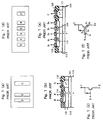
- Figs. 1(a) through 1(f) of the accompanying drawings show bipolar transistors disclosed in Japanese laid-open patent publication No. 7-254608.
- Figs. 1(a) through 1(c) are plan and cross-sectional views and an equivalent circuit diagram, respectively, of a bipolar transistor having a single emitter structure
- Figs. 1(d) through 1(f) are plan and cross-sectional views and an equivalent circuit diagram, respectively, of a bipolar transistor having a multiple emitter structure.
- Figs. 1(a) through 1(f) of the accompanying drawings show bipolar transistors disclosed in Japanese laid-open patent publication No. 7-254608.
- Figs. 1(a) through 1(c) are plan and cross-sectional views and an equivalent circuit diagram, respectively, of a bipolar transistor having a single emitter structure
- Figs. 1(d) through 1(f) are plan and cross-sectional views and an equivalent circuit diagram, respectively, of a bipolar transistor having a multiple emitter structure.
- an n + embedded layer 111 and an n collector layer 112 are successively disposed on a p Si substrate 110, and a base layer 113, an emitter layer 114, and a device separating insulative film 115 are successively disposed on the n collector layer 112.
- a single emitter layer 114 is disposed in the base layer 113.
- two emitter layers 114 are disposed in the base layer 113.
- Each of the emitter layers 114 of the multiple emitter structure has a width half the width of the emitter layer 114 of the single emitter structure.
- the total emitter area of the single emitter structure is the same as the total emitter area of the multiple emitter structure.
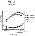
- Fig. 2 of the accompanying drawings shows the relationship between the collector current, and the noise figures and power gain of the conventional bipolar transistors shown in Figs. 1(a) through 1(f).
- the multiple emitter bipolar transistor having the plural emitters has a lower noise figure than the single emitter bipolar transistor having the single emitter in a certain collector current range.
- the power gain of the single emitter bipolar transistor is better than the multiple emitter bipolar transistor in all collector current ranges. Instead of improving these noise figure and power gain characteristics through device and circuit approaches, these two bipolar transistors are simply used in different circuits.
- the conventional bipolar transistors suffer the following disadvantages:
- the total emitter area in the single emitter bipolar transistor is the same as the total emitter area in the multiple emitter bipolar transistor. That is, these bipolar transistor have different emitter lengths, indicating that there are a plurality of bipolar transistors having different emitter structures in a circuit.
- the conventional bipolar transistors are not of a so-called self-aligned structure with a base region constructed of polycrystalline silicon or the like.
- a base region constructed of polycrystalline silicon it is important for bipolar transistors which operate in a high-frequency range such as a GHz range to have improved high-frequency characteristics by reducing the base resistance. Therefore, bipolar transistors with a base electrode constructed of polycrystalline silicon are more preferable in terms of a noise figure and a power gain than the conventional non-self-aligned bipolar transistors.
- Bipolar transistors having a shorter emitter width tend to suffer a plug effect on emitters because the aspect ratio of an emitter contact is greater than the non-self-aligned bipolar transistors.
- the plug effect is a phenomenon in which when an impurity is diffused from an emitter region, the impurity is subject to less diffusion in a transistor structure with a smaller emitter width than in a transistor structure with a greater emitter width.
- the thermal history of a transistor is adjusted in the fabrication process to optimize the depth of an emitter-to-base junction of a transistor structure with a smaller emitter width in view of the plug effect. Therefore, in a transistor structure with a greater emitter width, an emitter impurity is diffused more deeply due to the plug effect, tending to cause a punchthrough between the emitter and the collector. For this reason, it is important to employ a single fixed transistor size in a circuit for the stable fabrication of transistors with a high yield.
- a semiconductor integrated circuit device comprising a multiple-stage amplifier including a plurality of transistors, the multiple-stage amplifier having a first stage comprising a plurality of bipolar transistors each having a single emitter structure, the bipolar transistors being connected parallel to each other.
- the bipolar transistors may have a common collector.
- Each of the bipolar transistors may comprise a self-aligned bipolar transistor having an emitter electrode and a base electrode which are made of polycrystalline silicon.
- Each of the bipolar transistors may have an emitter having a length ranging from 20 to 30 ⁇ m and a width ranging from 0.5 to 0.8 ⁇ m.
- a method of designing a semiconductor integrated circuit device having a multiple-stage amplifier including a plurality of transistors comprising the step of constructing a first stage of the multiple-stage amplifier of a plurality of bipolar transistors each having a single emitter structure, the bipolar transistors being connected parallel to each other.
- the semiconductor integrated circuit device offers such an advantage, and is capable of amplifying an input signal with a reduced noise level.
- Fig. 3 of the accompanying drawings shows the relationship between the total collector current I c (mA) and noise figure NF min (dB) of bipolar transistors.
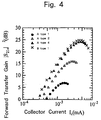
- Fig. 4 of the accompanying drawings shows the relationship between the collector current I c (mA) and forward transfer gain
- type A represents a bipolar transistor having an emitter width of 0.8 ⁇ m and an emitter length of 1.6 ⁇ m
- type B represents a bipolar transistor having an emitter width of 0.8 ⁇ m and an emitter length of 6.4 ⁇ m.
- the number associated with type A and type B indicates the number of parallel-connected transistors.
- Figs. 3 and 4 show the transistor type B having a single emitter structure whose emitter area is the same as the emitter area of a structure composed of four parallel-connected minimum transistors type A.
- a comparison between these structures indicate that the forward transfer gain of the single emitter structure is slightly better than the forward transfer gain of the structure composed of four parallel-connected minimum transistors type A, as shown in Fig. 4, whereas the noise level of the structure composed of four parallel-connected minimum transistors type A is lower than the noise level of the single emitter structure, as shown in Fig. 3.
- the forward transfer gain is maintained at an original level of is at least 25 dB, the gain difference between the transistors of low-noise amplifiers is not significant, but reducing the noise figure is more advantageous.
- Amplifiers in most integrated circuits are designed in multiple stages. In each stage, the amplifier performs the function of a voltage gain, a current gain, or an input-to-output impedance conversion. In general, it is widely practiced to connect amplifiers in cascade for increasing the overall amplification factor. Specifically, a plurality of amplifiers having different noise figures and power gains are connected in cascade.
- bipolar transistors of the first-stage amplifier which are of a single emitter structure and have the same emitter size, are connected parallel to each other, then the resultant integrated circuit has best power gain characteristics and noise characteristics.
- Figs. 5(a) through 5(c) show a basic transistor for use in an amplifier according to a first embodiment of the present invention.
- Fig. 5(a) is a plan view of the basic transistor which is of a single emitter structure
- Fig. 5(b) is a cross-sectional view of the basic transistor.
- the basic transistor comprises a base (B) diffusion layer 1, a collector (C) diffusion layer 2, a base polysilicon region 3, an emitter (E) polysilicon region 4, a contact 5 on the base polysilicon region 3, a contact 6 on the emitter polysilicon region 4, a contact 7 on the collector diffusion layer 2, a p + embedded layer 8, a p well 9, an Si substrate 10, a device separating insulative film 15, and an interlayer insulative film 16.
- the transistor is of a so-called self-aligned structure with a base region constructed of polycrystalline silicon or the like.
- the p + embedded layer 8 and the p well 9 are provided for separating the device of the bipolar transistor, and are disposed in surrounding relation to the bipolar transistor.
- Fig. 5(c) is a view showing three parallel-connected transistors each having the same size as the basic transistor shown in Figs. 5(a) and 5(b).
- the bases, emitters, and collectors of the three parallel-connected transistors are interconnected by aluminum interconnections 17.
- Fig. 6(a) is a circuit diagram of an amplifier which incorporates the transistors according to the present invention.
- the amplifier comprises a two-stage emitter-grounded amplifier and an emitter-follower buffer.
- An input signal applied from a signal source to an input terminal IN is supplied to a capacitor C1, which cuts off a DC component from the input signal.
- the input signal is then supplied to the amplifier which comprises transistors Q1, Q2.
- Resistors R1 - R6 serve to give self biases to the transistors Q1, Q2, and capacitors C1, C2 serve to prevent the amplification factor from being lowered for high-frequency compensation.
- the emitter-follower buffer comprises a transistor Q3 and a resistor R7 for ensuring a sufficient current for operating a next circuit.
- the transistor Q1 is shown as a single transistor in Fig. 6(a), but actually comprises three transistors Q connected parallel to each other, as shown in Fig. 6(b), the transistors Q being of the same structure and size as the transistors Q2, Q3. If the transistor Q2 were of the same structure as the transistor Q1, then the noise figure of the amplifier would be increased. Therefore, only the first stage of the amplifier comprises parallel-connected transistors.
- Figs. 7(a) and 7(b) show layouts of the amplifier on a silicon substrate. Specifically, Fig. 7(a) illustrates a layout of transistors Q1 - Q3, resistors R1 - R7, and capacitors C1 - C4. The transistors and the capacitors of the two-stage amplifier are indicated as enclosed by dotted lines, and connected parallel to each other, making up the amplifier.
- Fig. 7(b) illustrates the manner in which the components are connected. It can be seen from Fig. 7(b) that since the capacitors take up a much larger area than the transistors, any increase in the area due to the parallel connection of the transistors of the two-stage amplifier poses almost no problem.
- Figs. 8(a) through 8(c) show transistors for use in an amplifier according to a second embodiment of the present invention.
- Figs. 8(a) through 8(c) two transistors having a common collector in a substrate are used as a basic component. These transistors which are connected parallel to each other are used in a first stage of an amplifier. Various parts of the transistors which are identical to those of the transistor shown in Figs. 5(a) through 5(c) are denoted by identical reference numerals, and will not be described in detail below.
- the area occupied by the transistors is reduced, and the number of parallel-connected transistors is increased.
- Figs. 9(a) and 9(b) show how a noise figure varies depending on the emitter size of a transistor. Specifically, Fig. 9(a) shows the dependency of the relationship between a noise figure and a collector current on an emitter length, and Fig. 9(b) shows the dependency of the relationship between a noise figure and a collector current on an emitter width.
- a dotted-line reference curve shifts to a solid-line curve when the emitter length and the emitter width increase, and shifts to a dot-and-dash-line curve when the emitter length and the emitter width decrease. These curve shifts correspond to changes in the base resistance and the collector-to-base and base-to-emitter parasitic capacitances.
- the emitter length is in trade-off relation to the power gain and the noise figure.
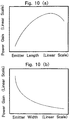
- Figs. 10(a) and 10(b) show the dependency of a power gain on the emitter size of a transistor. Specifically, Fig. 10(a) shows the dependency of a power gain on an emitter length, and Fig. 10(b0 shows the dependency of a power gain on an emitter width.
- a study of Fig. 10(a) indicates that as the emitter length increases, the power gain increases, but the power gain starts to decrease at a certain emitter length. This is because as the emitter length increases, the overall size of the transistor increases, causing an increase in the parasitic capacitance to exceed a reduction in the base resistance.
- the power gain decreases continuously. This is because the parasitic capacitance and the base resistance increase as the emitter width increases.
- the emitter length is determined depending on the value to which the collector current is to be set in order to reduce the noise figure and increase the power gain.
- the emitter width is preferably as small as possible, it is determined depending on the plug effect of the emitter. According to an experiment conducted by the inventor, a most suitable actual emitter size was 20 - 30 ⁇ m in terms of an emitter length and 0.5 - 0.8 ⁇ m in terms of an emitter width. However, these values vary with the layout of bipolar transistors because they are determined depending on a balance between the parasitic capacitance and the parasitic resistance.
- the semiconductor integrated circuit device according to the present invention offers the following advantages:
- the semiconductor integrated circuit device Since there is only one basic transistor, the semiconductor integrated circuit device can be easily designed.
- Circuits can be designed in a short period of time because no process is required to use single emitter and multiple emitter transistors in respective circuits.
Landscapes
- Bipolar Transistors (AREA)
- Bipolar Integrated Circuits (AREA)
- Semiconductor Integrated Circuits (AREA)
- Amplifiers (AREA)
Applications Claiming Priority (3)
| Application Number | Priority Date | Filing Date | Title |
|---|---|---|---|
| JP9264342A JPH11102916A (ja) | 1997-09-29 | 1997-09-29 | 半導体集積回路装置およびその設計方法 |
| JP26434297 | 1997-09-29 | ||
| JP264342/97 | 1997-09-29 |
Publications (2)
| Publication Number | Publication Date |
|---|---|
| EP0905769A2 true EP0905769A2 (de) | 1999-03-31 |
| EP0905769A3 EP0905769A3 (de) | 2001-10-17 |
Family
ID=17401841
Family Applications (1)
| Application Number | Title | Priority Date | Filing Date |
|---|---|---|---|
| EP98118196A Withdrawn EP0905769A3 (de) | 1997-09-29 | 1998-09-25 | Integriertes halbleiterbasiertes Schaltkreisbauelement mit bipolaren Transistoren und deren Herstellungsverfahren |
Country Status (5)
| Country | Link |
|---|---|
| US (1) | US6300669B1 (de) |
| EP (1) | EP0905769A3 (de) |
| JP (1) | JPH11102916A (de) |
| KR (1) | KR100335330B1 (de) |
| CN (1) | CN1213180A (de) |
Cited By (1)
| Publication number | Priority date | Publication date | Assignee | Title |
|---|---|---|---|---|
| EP1061572A1 (de) * | 1999-06-16 | 2000-12-20 | STMicroelectronics S.r.l. | Integrierte Struktur für Radiofrequenzanwendungen |
Families Citing this family (12)
| Publication number | Priority date | Publication date | Assignee | Title |
|---|---|---|---|---|
| JP2002076014A (ja) | 2000-08-30 | 2002-03-15 | Mitsubishi Electric Corp | 高周波用半導体装置 |
| JP4489366B2 (ja) * | 2003-03-17 | 2010-06-23 | 株式会社日立製作所 | 半導体装置 |
| CN100339946C (zh) * | 2004-12-22 | 2007-09-26 | 中国电子科技集团公司第二十四研究所 | 小比导通电阻的集成化大电流功率器件结构的设计方法 |
| US7816988B2 (en) * | 2006-02-03 | 2010-10-19 | Honglei Wu | Amplifier |
| JP5503168B2 (ja) * | 2009-03-19 | 2014-05-28 | 株式会社日立製作所 | 半導体集積回路装置 |
| CN102025354A (zh) * | 2009-09-23 | 2011-04-20 | 鸿富锦精密工业(深圳)有限公司 | 时序控制电路 |
| CN103176922A (zh) * | 2011-12-23 | 2013-06-26 | 鸿富锦精密工业(深圳)有限公司 | Usb识别电路 |
| CN103176936A (zh) * | 2011-12-26 | 2013-06-26 | 鸿富锦精密工业(深圳)有限公司 | 接口控制电路 |
| CN104063030A (zh) * | 2013-03-22 | 2014-09-24 | 鸿富锦精密电子(天津)有限公司 | 开机电路 |
| CN106155179A (zh) * | 2015-04-23 | 2016-11-23 | 鸿富锦精密工业(武汉)有限公司 | 杂波信号滤除电路 |
| JP2018011181A (ja) | 2016-07-13 | 2018-01-18 | 株式会社村田製作所 | 検波回路 |
| JP6710606B2 (ja) * | 2016-08-23 | 2020-06-17 | 株式会社村田製作所 | 高周波増幅器モジュール |
Family Cites Families (14)
| Publication number | Priority date | Publication date | Assignee | Title |
|---|---|---|---|---|
| JPS5228842A (en) | 1975-08-29 | 1977-03-04 | Nippon Gakki Seizo Kk | Small signal amplification circuit |
| JPS53117984A (en) | 1978-01-20 | 1978-10-14 | Hitachi Ltd | Amplifier |
| US4400865A (en) * | 1980-07-08 | 1983-08-30 | International Business Machines Corporation | Self-aligned metal process for integrated circuit metallization |
| JPS60137057A (ja) * | 1983-12-26 | 1985-07-20 | Matsushita Electronics Corp | 微小信号増幅装置 |
| GB2179201B (en) * | 1985-08-14 | 1990-01-17 | Mitsubishi Electric Corp | Method for fabricating a semiconductor device |
| JPH0246010A (ja) * | 1988-08-08 | 1990-02-15 | N S:Kk | 広帯域増幅器 |
| JPH07109831B2 (ja) * | 1990-01-25 | 1995-11-22 | 株式会社東芝 | 半導体装置 |
| DE4024166C1 (de) * | 1990-07-30 | 1991-12-19 | Siemens Ag, 8000 Muenchen, De | |
| JPH05291834A (ja) * | 1992-04-09 | 1993-11-05 | Pioneer Electron Corp | 電力増幅器 |
| JP3033372B2 (ja) | 1992-11-25 | 2000-04-17 | 日本電気株式会社 | 半導体装置 |
| JPH07254608A (ja) | 1994-03-15 | 1995-10-03 | Toshiba Corp | 半導体装置 |
| JPH09199513A (ja) * | 1996-01-19 | 1997-07-31 | Mitsubishi Electric Corp | バイポーラトランジスタおよび該バイポーラトランジスタを有する半導体装置 |
| US5896062A (en) * | 1997-03-21 | 1999-04-20 | Northern Telecom Limited | Amplifier with switched DC bias voltage feedback |
| JP3104652B2 (ja) * | 1997-09-05 | 2000-10-30 | 日本電気株式会社 | 発振回路 |
-
1997
- 1997-09-29 JP JP9264342A patent/JPH11102916A/ja active Pending
-
1998
- 1998-09-25 US US09/160,040 patent/US6300669B1/en not_active Expired - Fee Related
- 1998-09-25 EP EP98118196A patent/EP0905769A3/de not_active Withdrawn
- 1998-09-25 CN CN98119393A patent/CN1213180A/zh active Pending
- 1998-09-25 KR KR1019980039979A patent/KR100335330B1/ko not_active Expired - Fee Related
Cited By (1)
| Publication number | Priority date | Publication date | Assignee | Title |
|---|---|---|---|---|
| EP1061572A1 (de) * | 1999-06-16 | 2000-12-20 | STMicroelectronics S.r.l. | Integrierte Struktur für Radiofrequenzanwendungen |
Also Published As
| Publication number | Publication date |
|---|---|
| KR19990030158A (ko) | 1999-04-26 |
| CN1213180A (zh) | 1999-04-07 |
| EP0905769A3 (de) | 2001-10-17 |
| US6300669B1 (en) | 2001-10-09 |
| KR100335330B1 (ko) | 2002-10-12 |
| JPH11102916A (ja) | 1999-04-13 |
Similar Documents
| Publication | Publication Date | Title |
|---|---|---|
| US6300669B1 (en) | Semiconductor integrated circuit device and method of designing same | |
| US5227734A (en) | Broadband bipolar transistor distributed amplifier | |
| JPH09246877A (ja) | 低ノイズ・高直線性のhemt−hbt複合装置 | |
| JP3952400B2 (ja) | 高周波用半導体装置 | |
| Stärke et al. | A 24.7 dB low noise amplifier with variable gain and tunable matching in 130 nm SiGe at 200 GHz | |
| Moradinia et al. | A SiGe HBT D-band LNA utilizing asymmetric broadside coupled lines | |
| JP2002076014A (ja) | 高周波用半導体装置 | |
| KR20020000804A (ko) | 실리콘 바이폴라 전력 고주파 트랜지스터 제조 방법 및 rf 전력 트랜지스터 장치 | |
| US12494749B2 (en) | Power amplifier | |
| US4245231A (en) | Combination capacitor and transistor structure for use in monolithic circuits | |
| Kobayashi et al. | A novel monolithic LNA integrating a common-source HEMT with an HBT Darlington amplifier | |
| US6784747B1 (en) | Amplifier circuit | |
| JP2004274430A (ja) | 電力増幅器モジュール及びその製造方法 | |
| US7902635B2 (en) | High-power-gain, bipolar transistor amplifier | |
| JP2002530871A (ja) | SiGeRFパワートランジスタにおけるエミッタ分割方法及びシステム | |
| US5654662A (en) | Inverted BJT current sources/sinks in RF circuits and methods | |
| JPS6228089Y2 (de) | ||
| EP1033811A3 (de) | Monolithischer fester aktiver Entzerrer, | |
| CN120090571A (zh) | 半导体装置 | |
| JP3136698B2 (ja) | 半導体集積回路 | |
| JPS6022530B2 (ja) | 電力増幅器 | |
| JPH05315550A (ja) | 増幅回路 | |
| JPWO2002056368A1 (ja) | 高周波電力増幅装置及び無線通信装置 | |
| JPH06326530A (ja) | 高出力増幅器 | |
| JPH1075136A (ja) | 半導体集積回路 |
Legal Events
| Date | Code | Title | Description |
|---|---|---|---|
| PUAI | Public reference made under article 153(3) epc to a published international application that has entered the european phase |
Free format text: ORIGINAL CODE: 0009012 |
|
| AK | Designated contracting states |
Kind code of ref document: A2 Designated state(s): AT BE CH CY DE DK ES FI FR GB GR IE IT LI LU MC NL PT SE Kind code of ref document: A2 Designated state(s): DE FR GB |
|
| AX | Request for extension of the european patent |
Free format text: AL;LT;LV;MK;RO;SI |
|
| PUAL | Search report despatched |
Free format text: ORIGINAL CODE: 0009013 |
|
| AK | Designated contracting states |
Kind code of ref document: A3 Designated state(s): AT BE CH CY DE DK ES FI FR GB GR IE IT LI LU MC NL PT SE |
|
| AX | Request for extension of the european patent |
Free format text: AL;LT;LV;MK;RO;SI |
|
| RIC1 | Information provided on ipc code assigned before grant |
Free format text: 7H 01L 21/8222 A, 7H 01L 21/331 B, 7H 01L 27/06 B, 7H 01L 27/082 B, 7H 03F 1/26 B |
|
| 17P | Request for examination filed |
Effective date: 20020213 |
|
| AKX | Designation fees paid |
Free format text: DE FR GB |
|
| RAP1 | Party data changed (applicant data changed or rights of an application transferred) |
Owner name: NEC ELECTRONICS CORPORATION |
|
| STAA | Information on the status of an ep patent application or granted ep patent |
Free format text: STATUS: THE APPLICATION HAS BEEN WITHDRAWN |
|
| 18W | Application withdrawn |
Effective date: 20040910 |