EP0907199A2 - Verdrahtungssubstrat und Gasentladungs-Anzeigevorrichtung - Google Patents
Verdrahtungssubstrat und Gasentladungs-Anzeigevorrichtung Download PDFInfo
- Publication number
- EP0907199A2 EP0907199A2 EP98118551A EP98118551A EP0907199A2 EP 0907199 A2 EP0907199 A2 EP 0907199A2 EP 98118551 A EP98118551 A EP 98118551A EP 98118551 A EP98118551 A EP 98118551A EP 0907199 A2 EP0907199 A2 EP 0907199A2
- Authority
- EP
- European Patent Office
- Prior art keywords
- electrodes
- layer
- resist
- gas discharge
- display device
- Prior art date
- Legal status (The legal status is an assumption and is not a legal conclusion. Google has not performed a legal analysis and makes no representation as to the accuracy of the status listed.)
- Granted
Links
- 239000000758 substrate Substances 0.000 title claims abstract description 70
- 229910010272 inorganic material Inorganic materials 0.000 claims abstract description 69
- 239000011147 inorganic material Substances 0.000 claims abstract description 69
- 238000001039 wet etching Methods 0.000 claims abstract description 29
- 238000000034 method Methods 0.000 claims description 78
- 238000005530 etching Methods 0.000 claims description 45
- 239000000463 material Substances 0.000 claims description 29
- VYPSYNLAJGMNEJ-UHFFFAOYSA-N Silicium dioxide Chemical compound O=[Si]=O VYPSYNLAJGMNEJ-UHFFFAOYSA-N 0.000 claims description 22
- 229910052681 coesite Inorganic materials 0.000 claims description 11
- 229910052906 cristobalite Inorganic materials 0.000 claims description 11
- 239000000377 silicon dioxide Substances 0.000 claims description 11
- 229910052682 stishovite Inorganic materials 0.000 claims description 11
- 229910052905 tridymite Inorganic materials 0.000 claims description 11
- 229910018487 Ni—Cr Inorganic materials 0.000 claims description 9
- 239000011810 insulating material Substances 0.000 claims description 2
- 239000010410 layer Substances 0.000 description 243
- 239000000243 solution Substances 0.000 description 30
- 239000010408 film Substances 0.000 description 24
- 230000007547 defect Effects 0.000 description 16
- 239000011521 glass Substances 0.000 description 15
- 230000007797 corrosion Effects 0.000 description 13
- 238000005260 corrosion Methods 0.000 description 13
- 239000007864 aqueous solution Substances 0.000 description 11
- 229920002120 photoresistant polymer Polymers 0.000 description 10
- 230000015572 biosynthetic process Effects 0.000 description 9
- 238000010586 diagram Methods 0.000 description 9
- 238000004544 sputter deposition Methods 0.000 description 9
- 239000010409 thin film Substances 0.000 description 9
- 238000011282 treatment Methods 0.000 description 9
- 238000004519 manufacturing process Methods 0.000 description 8
- 229910045601 alloy Inorganic materials 0.000 description 7
- 239000000956 alloy Substances 0.000 description 7
- 229910052759 nickel Inorganic materials 0.000 description 7
- QAOWNCQODCNURD-UHFFFAOYSA-N Sulfuric acid Chemical compound OS(O)(=O)=O QAOWNCQODCNURD-UHFFFAOYSA-N 0.000 description 6
- 229910052804 chromium Inorganic materials 0.000 description 5
- 239000011368 organic material Substances 0.000 description 5
- VTYYLEPIZMXCLO-UHFFFAOYSA-L Calcium carbonate Chemical compound [Ca+2].[O-]C([O-])=O VTYYLEPIZMXCLO-UHFFFAOYSA-L 0.000 description 4
- 239000004115 Sodium Silicate Substances 0.000 description 4
- 238000006243 chemical reaction Methods 0.000 description 4
- 238000007796 conventional method Methods 0.000 description 4
- 239000000395 magnesium oxide Substances 0.000 description 4
- CPLXHLVBOLITMK-UHFFFAOYSA-N magnesium oxide Inorganic materials [Mg]=O CPLXHLVBOLITMK-UHFFFAOYSA-N 0.000 description 4
- AXZKOIWUVFPNLO-UHFFFAOYSA-N magnesium;oxygen(2-) Chemical compound [O-2].[Mg+2] AXZKOIWUVFPNLO-UHFFFAOYSA-N 0.000 description 4
- 239000012286 potassium permanganate Substances 0.000 description 4
- 235000019795 sodium metasilicate Nutrition 0.000 description 4
- NTHWMYGWWRZVTN-UHFFFAOYSA-N sodium silicate Chemical compound [Na+].[Na+].[O-][Si]([O-])=O NTHWMYGWWRZVTN-UHFFFAOYSA-N 0.000 description 4
- 229910052911 sodium silicate Inorganic materials 0.000 description 4
- 230000000694 effects Effects 0.000 description 3
- 238000001704 evaporation Methods 0.000 description 3
- RUTXIHLAWFEWGM-UHFFFAOYSA-H iron(3+) sulfate Chemical compound [Fe+3].[Fe+3].[O-]S([O-])(=O)=O.[O-]S([O-])(=O)=O.[O-]S([O-])(=O)=O RUTXIHLAWFEWGM-UHFFFAOYSA-H 0.000 description 3
- 229910000360 iron(III) sulfate Inorganic materials 0.000 description 3
- 238000005192 partition Methods 0.000 description 3
- 238000007639 printing Methods 0.000 description 3
- XOLBLPGZBRYERU-UHFFFAOYSA-N tin dioxide Chemical compound O=[Sn]=O XOLBLPGZBRYERU-UHFFFAOYSA-N 0.000 description 3
- -1 ITO Substances 0.000 description 2
- 239000003513 alkali Substances 0.000 description 2
- 229910052782 aluminium Inorganic materials 0.000 description 2
- 229910000019 calcium carbonate Inorganic materials 0.000 description 2
- 239000000356 contaminant Substances 0.000 description 2
- 230000002950 deficient Effects 0.000 description 2
- 238000007599 discharging Methods 0.000 description 2
- 238000001312 dry etching Methods 0.000 description 2
- 230000008020 evaporation Effects 0.000 description 2
- 229910052737 gold Inorganic materials 0.000 description 2
- 230000009257 reactivity Effects 0.000 description 2
- 238000007789 sealing Methods 0.000 description 2
- 229910052709 silver Inorganic materials 0.000 description 2
- 229910017813 Cu—Cr Inorganic materials 0.000 description 1
- 230000002378 acidificating effect Effects 0.000 description 1
- 230000004888 barrier function Effects 0.000 description 1
- 239000004020 conductor Substances 0.000 description 1
- 238000010276 construction Methods 0.000 description 1
- 239000007772 electrode material Substances 0.000 description 1
- 238000003912 environmental pollution Methods 0.000 description 1
- 238000002474 experimental method Methods 0.000 description 1
- 238000010304 firing Methods 0.000 description 1
- AMGQUBHHOARCQH-UHFFFAOYSA-N indium;oxotin Chemical compound [In].[Sn]=O AMGQUBHHOARCQH-UHFFFAOYSA-N 0.000 description 1
- 238000004020 luminiscence type Methods 0.000 description 1
- 230000003446 memory effect Effects 0.000 description 1
- 239000002245 particle Substances 0.000 description 1
- 239000012466 permeate Substances 0.000 description 1
- 238000000206 photolithography Methods 0.000 description 1
- 230000002265 prevention Effects 0.000 description 1
- 239000011241 protective layer Substances 0.000 description 1
- 238000004528 spin coating Methods 0.000 description 1
- 229910001887 tin oxide Inorganic materials 0.000 description 1
Images




Classifications
-
- H—ELECTRICITY
- H01—ELECTRIC ELEMENTS
- H01J—ELECTRIC DISCHARGE TUBES OR DISCHARGE LAMPS
- H01J17/00—Gas-filled discharge tubes with solid cathode
-
- H—ELECTRICITY
- H05—ELECTRIC TECHNIQUES NOT OTHERWISE PROVIDED FOR
- H05K—PRINTED CIRCUITS; CASINGS OR CONSTRUCTIONAL DETAILS OF ELECTRIC APPARATUS; MANUFACTURE OF ASSEMBLAGES OF ELECTRICAL COMPONENTS
- H05K3/00—Apparatus or processes for manufacturing printed circuits
- H05K3/02—Apparatus or processes for manufacturing printed circuits in which the conductive material is applied to the surface of the insulating support and is thereafter removed from such areas of the surface which are not intended for current conducting or shielding
- H05K3/06—Apparatus or processes for manufacturing printed circuits in which the conductive material is applied to the surface of the insulating support and is thereafter removed from such areas of the surface which are not intended for current conducting or shielding the conductive material being removed chemically or electrolytically, e.g. by photo-etch process
- H05K3/061—Etching masks
- H05K3/062—Etching masks consisting of metals or alloys or metallic inorganic compounds
-
- H—ELECTRICITY
- H01—ELECTRIC ELEMENTS
- H01J—ELECTRIC DISCHARGE TUBES OR DISCHARGE LAMPS
- H01J11/00—Gas-filled discharge tubes with alternating current induction of the discharge, e.g. alternating current plasma display panels [AC-PDP]; Gas-filled discharge tubes without any main electrode inside the vessel; Gas-filled discharge tubes with at least one main electrode outside the vessel
- H01J11/10—AC-PDPs with at least one main electrode being out of contact with the plasma
- H01J11/12—AC-PDPs with at least one main electrode being out of contact with the plasma with main electrodes provided on both sides of the discharge space
-
- H—ELECTRICITY
- H01—ELECTRIC ELEMENTS
- H01J—ELECTRIC DISCHARGE TUBES OR DISCHARGE LAMPS
- H01J11/00—Gas-filled discharge tubes with alternating current induction of the discharge, e.g. alternating current plasma display panels [AC-PDP]; Gas-filled discharge tubes without any main electrode inside the vessel; Gas-filled discharge tubes with at least one main electrode outside the vessel
- H01J11/20—Constructional details
- H01J11/22—Electrodes, e.g. special shape, material or configuration
-
- H—ELECTRICITY
- H01—ELECTRIC ELEMENTS
- H01J—ELECTRIC DISCHARGE TUBES OR DISCHARGE LAMPS
- H01J11/00—Gas-filled discharge tubes with alternating current induction of the discharge, e.g. alternating current plasma display panels [AC-PDP]; Gas-filled discharge tubes without any main electrode inside the vessel; Gas-filled discharge tubes with at least one main electrode outside the vessel
- H01J11/20—Constructional details
- H01J11/22—Electrodes, e.g. special shape, material or configuration
- H01J11/24—Sustain electrodes or scan electrodes
-
- H—ELECTRICITY
- H01—ELECTRIC ELEMENTS
- H01J—ELECTRIC DISCHARGE TUBES OR DISCHARGE LAMPS
- H01J9/00—Apparatus or processes specially adapted for the manufacture, installation, removal, maintenance of electric discharge tubes, discharge lamps, or parts thereof; Recovery of material from discharge tubes or lamps
- H01J9/02—Manufacture of electrodes or electrode systems
-
- H—ELECTRICITY
- H01—ELECTRIC ELEMENTS
- H01J—ELECTRIC DISCHARGE TUBES OR DISCHARGE LAMPS
- H01J2211/00—Plasma display panels with alternate current induction of the discharge, e.g. AC-PDPs
- H01J2211/20—Constructional details
- H01J2211/22—Electrodes
- H01J2211/225—Material of electrodes
-
- H—ELECTRICITY
- H05—ELECTRIC TECHNIQUES NOT OTHERWISE PROVIDED FOR
- H05K—PRINTED CIRCUITS; CASINGS OR CONSTRUCTIONAL DETAILS OF ELECTRIC APPARATUS; MANUFACTURE OF ASSEMBLAGES OF ELECTRICAL COMPONENTS
- H05K2201/00—Indexing scheme relating to printed circuits covered by H05K1/00
- H05K2201/01—Dielectrics
- H05K2201/0137—Materials
- H05K2201/0175—Inorganic, non-metallic layer, e.g. resist or dielectric for printed capacitor
-
- H—ELECTRICITY
- H05—ELECTRIC TECHNIQUES NOT OTHERWISE PROVIDED FOR
- H05K—PRINTED CIRCUITS; CASINGS OR CONSTRUCTIONAL DETAILS OF ELECTRIC APPARATUS; MANUFACTURE OF ASSEMBLAGES OF ELECTRICAL COMPONENTS
- H05K2201/00—Indexing scheme relating to printed circuits covered by H05K1/00
- H05K2201/03—Conductive materials
- H05K2201/032—Materials
- H05K2201/0326—Inorganic, non-metallic conductor, e.g. indium-tin oxide [ITO]
-
- H—ELECTRICITY
- H05—ELECTRIC TECHNIQUES NOT OTHERWISE PROVIDED FOR
- H05K—PRINTED CIRCUITS; CASINGS OR CONSTRUCTIONAL DETAILS OF ELECTRIC APPARATUS; MANUFACTURE OF ASSEMBLAGES OF ELECTRICAL COMPONENTS
- H05K2203/00—Indexing scheme relating to apparatus or processes for manufacturing printed circuits covered by H05K3/00
- H05K2203/02—Details related to mechanical or acoustic processing, e.g. drilling, punching, cutting, using ultrasound
- H05K2203/025—Abrading, e.g. grinding or sand blasting
-
- H—ELECTRICITY
- H05—ELECTRIC TECHNIQUES NOT OTHERWISE PROVIDED FOR
- H05K—PRINTED CIRCUITS; CASINGS OR CONSTRUCTIONAL DETAILS OF ELECTRIC APPARATUS; MANUFACTURE OF ASSEMBLAGES OF ELECTRICAL COMPONENTS
- H05K2203/00—Indexing scheme relating to apparatus or processes for manufacturing printed circuits covered by H05K3/00
- H05K2203/10—Using electric, magnetic and electromagnetic fields; Using laser light
- H05K2203/107—Using laser light
-
- H—ELECTRICITY
- H05—ELECTRIC TECHNIQUES NOT OTHERWISE PROVIDED FOR
- H05K—PRINTED CIRCUITS; CASINGS OR CONSTRUCTIONAL DETAILS OF ELECTRIC APPARATUS; MANUFACTURE OF ASSEMBLAGES OF ELECTRICAL COMPONENTS
- H05K3/00—Apparatus or processes for manufacturing printed circuits
- H05K3/02—Apparatus or processes for manufacturing printed circuits in which the conductive material is applied to the surface of the insulating support and is thereafter removed from such areas of the surface which are not intended for current conducting or shielding
- H05K3/04—Apparatus or processes for manufacturing printed circuits in which the conductive material is applied to the surface of the insulating support and is thereafter removed from such areas of the surface which are not intended for current conducting or shielding the conductive material being removed mechanically, e.g. by punching
-
- H—ELECTRICITY
- H05—ELECTRIC TECHNIQUES NOT OTHERWISE PROVIDED FOR
- H05K—PRINTED CIRCUITS; CASINGS OR CONSTRUCTIONAL DETAILS OF ELECTRIC APPARATUS; MANUFACTURE OF ASSEMBLAGES OF ELECTRICAL COMPONENTS
- H05K3/00—Apparatus or processes for manufacturing printed circuits
- H05K3/38—Improvement of the adhesion between the insulating substrate and the metal
- H05K3/388—Improvement of the adhesion between the insulating substrate and the metal by the use of a metallic or inorganic thin film adhesion layer
Definitions
- This invention relates to a wiring substrate comprising a wiring substrate with a wiring pattern formed thereon, and a gas discharge display device using the same.
- Gas discharge display devices such as plasma display and the like make display through a self-luminescence, and therefore are characterized in that the field angle is large, the display is easy to see, the thickness can be lessened, and a large picture plane can be realized.
- gas discharge display devices have become applied to display devices of information terminal equipments and high-quality picture tubes of television.
- Plasma displays are roughly classified into direct current driving type and alternate current driving type. Among them, the alternate current type of plasma display shows a high luminance owing to the memory action of dielectric layer covering electrodes, and its lifetime has reached a practical level through formation of protective layer. This results in practical application of plasma displays to video monitors for many uses.
- Fig. 9 is a perspective view illustrating the structure of a practical plasma display panel, wherein the front side substrate 100 is shown apart from the back side substrate 200 for the purpose of facilitating understanding.
- the front side substrate 100 comprises a display electrode 600 made of a transparent conductive material such as ITO (indium tin oxide), tin oxide (SnO 2 ) or the like, a bus electrode 700 made of a low-resistance material, a dielectric layer 800 made of a transparent insulating material and a protecting layer 900 made of magnesium oxide (MgO) or the like, all being formed on a front side glass substrate 400.
- a display electrode 600 made of a transparent conductive material such as ITO (indium tin oxide), tin oxide (SnO 2 ) or the like
- a bus electrode 700 made of a low-resistance material
- dielectric layer 800 made of a transparent insulating material
- a protecting layer 900 made of magnesium oxide (MgO) or the like
- the back side substrate 200 comprises an address electrode 1000, a barrier rib 1100 and a fluorescent material layer 1200, all formed on a back side glass substrate 500. Although not shown in Fig. 9, a dielectric layer 1300 is formed on the address electrode 1000, too.
- a discharge space region 300 is formed between the front side substrate 100 and the back glass side substrate 500.
- an alternate current voltage is applied between one pair of display electrodes 600 provided on the front side substrate 100, and a voltage is applied between the address electrode 1000 provided on the back side substrate 200 and the display electrode 600, whereby an address discharge is made to occur and a main discharge is generated in a prescribed discharging cell.
- the main discharge generates an ultraviolet ray, which induces emission of lights from the red-, green- and blue-color fluorescent materials 1200 separately coated on respective discharging cells. A display is made by emission of these lights.
- Fig. 5, 8A-8O illustrate an exemplary process for forming address electrode 1000 on back side glass substrate 500. Explanation of the process for forming bus electrode 700 carried on front side substrate 100 is omitted, because it can be formed by a similar process.
- a Cr/Cu/Cr layer (1000a-c) for forming address electrode 1000 on the back side glass substrate 500 and a resist 2500 for forming the pattern of address electrode 1000 are successively piled lamination-wise by a film-forming technique such as sputtering, evaporation, spin coating, dry filling, etc.
- a film-forming technique such as sputtering, evaporation, spin coating, dry filling, etc.
- the resist 2500 is exposed to light and developed so as to form a desired pattern of address electrode 1000
- Fig. 8B and 8C Photolithographic step
- the Cr layer 1000a is etched to form the desired pattern
- Step (d) Fig. 8D: Etching step).
- wet etching The above-mentioned process using an etching solution is generally called "wet etching".
- the resist 2500 is formed from an organic material.
- a photolithographic step for forming a resist is indispensable.
- the present inventors have studied on a technique for forming a multi-layered wiring such as those having a structure of Cr layer 1000a/Cu layer 1000b/Cr layer 1000c, etc. by using only the resist 2500 formed by Steps (a)-(c).
- This technique may be realizable if an etching solution capable of selectively etching Cr layer or Cu layer is used.
- an etching solution capable of selectively etching Cr layer or Cu layer is used.
- Cr layers 1000a and 1000c are quite readily side-etched and accuracy of fabrication of the Cr/Cu/Cr layer is quite unstable, so far as an etching solution giving no damage to alkali-developable releasable resists is used.
- a Cr layer is side-etched, the side-etched portions form gaps, which incurs inclusion of voids and contaminants such as etching solution.
- the contaminants cause corrosion and breakage of wiring in the step of firing the dielectric. Occurrence of breakage in the wiring means existence of wire portions not contributing to display in a gas discharge display panel, which is a fatal problem to a display panel.
- Cr/Cu/Cr layer constitutes a wiring of lower resistance as compared with other electrode materials, it is quite useful for large-sized display devices such as gas discharge display panel and the like. But, the same problem as mentioned above arises also in case of forming a multi-layer wiring such as Cr/Al/Cr by the method of wet etching.
- the adhesion between resist and electrode is insufficient, which causes corrosion by etching solution at the resist interface. It has further been revealed that, in such a resist, extraneous materials and air bubbles are included to cause defects in resist, due to which corrosion and thereby caused breakage of wiring can occur. Further, since conventional resists have been formed by a photolithographic process, they are apt to have defects due to extraneous matter. If electrode is formed by wet etching from a resist including defects, the regions corresponding to the defects are similarly etched, which causes breakage of wiring. These problems arise not only in Cr/Cu/Cr type multi-layer wiring, but also in case of forming a wiring of Al, Ag, Ni, Au, etc. by wet etching.
- the object of this invention consists in suppressing the breakage of wiring in the case of forming electrodes by wet etching process.
- this invention forms a resist from an inorganic material in a wet etching process.
- this invention forms a gas discharge display device provided with a front side substrate having a plurality of first electrodes and a back side substrate having a plurality of second electrodes, wherein at least the first electrodes or the second electrodes are formed from a resist made of an inorganic material by wet etching process.
- this invention forms a gas discharge display device provided with a front side substrate having a plurality of first electrodes and a first dielectric layer covering said first electrodes, a back side substrate having a plurality of electrodes and a second dielectric layer covering said second electrodes and a layer of an inorganic material layer interposed at least between said first electrodes and said first dielectric layer or between said second electrodes and said second dielectric layer, wherein said first electrodes or said second electrodes are formed by wet etching process.
- a resist formed in the above-mentioned manner by forming an inorganic material into a film by sputtering or evaporation method has an increased adhesiveness to electrodes as compared with conventional resists made of organic material, such a resist is prevented from the corrosion by etching solution at the resist interface and thereby the breakage of wiring can be suppressed.
- an inorganic material is used as resist, such a resist does not require so much consideration for etching damage as in the use of conventional resists made of organic material, so that an etching solution facilitating the control of etching quantity can be used, and the breakage of wiring due to side etching occurring in the conventional technique can be prevented by the use of inexpensive inorganic material. That is, as the inorganic material, ITO, SiO 2 , Ni-Cr and the like can be used, for instance.
- the inorganic layer may be made to remain between the electrodes and dielectric layer instead of releasing the inorganic layer, and this makes it possible to prevent the corrosion of electrodes and breakage of wiring due to the reaction between electrodes and dielectric layer.
- any means such as photolithography, blaster, laser and the like may be used.
- the gas discharge display device of this invention comprises a front side substrate having a plurality of first electrodes and a back side substrate having a plurality of second electrodes, wherein at least said first electrodes or said second electrodes have thereon a material layer formed by means of blaster and said first electrodes or second electrodes are formed from said material layer by wet etching process.
- the material layer serves as a resist for the first or second electrodes.
- this invention forms the material layer (resist) by means of a blaster, etching solution does not permeate the interface between the protecting layer and the material layer, which lessens the risk of forming defects in the material layer (resist). This has made it possible to carry out the wet etching on a material having only a small number of defects and therefore to suppress breakage of electrodes.
- fabrication of a resist by means of blaster can be achieved in a short period of time at a low cost.
- the material layer is formed by means of laser instead of blaster, the formation of protecting layer necessary to the blaster process is unnecessary, due to which electrodes can be formed without photolithographic process and therefore the electrode-forming process can naturally be shortened to a great extent.
- the use of mask for forming an electrode pattern is unnecessary.
- the material layer (resist) is formed without photolithographic process, a partial removal of the material layer by means of laser is enough for obtaining a desired pattern, which makes it possible to decrease the number of defects in resist extremely.
- the material layer may be made of any of organic material and inorganic material.
- the same fabrication as achievable by means of laser can be achieved by throttling the nozzle.
- the same processing as in the case of using a laser is possible even if the material layer (resist) is subjected to mechanical cutting to obtain a desired electrode pattern.
- Figs. 1A-1H illustrate the first embodiment in which address electrodes are formed on a back side substrate.
- 10 is a back side glass substrate, and 11a, 11b and 11c are address electrodes in which Cr/Cu/Cr layers are successively laminated.
- 25 is an inorganic material layer functioning as a resist, and 26 is a photoresist layer for forming a pattern of resist 25.
- the photoresist 26 (dry film resist) is exposed to light and developed so as to give a desired electrode pattern, and then baked (Step (b), Fig. 1B).
- This fabrication of resist by blast treatment makes it possible to form a pattern having an approximately same width as that of resist with a very high accuracy in a very short period of time.
- the photoresist 26 (dry film resist) is peeled off (Step (e), Fig. 1E). It is preferable at this time to wash away the dusts of inorganic material layer (ITO layer) formed upon the above-mentioned blast treatment.
- Cr layer 11a is etched with an aqueous solution containing potassium permanganate and sodium metasilicate (Step (f), Fig. 1F).
- the above-mentioned inorganic material layer 25 acts as a resist for Cr layer 11a.
- the aqueous solution containing potassium permanganate and sodium metasilicate is an alkaline aqueous solution which can etch the Cr layer 11a, while it scarcely etches the inorganic material layer 25 (ITO layer) and the Cu layer 11b.
- the inorganic material layer 25 (ITO layer) is not substantially corroded by the alkaline aqueous solution, and the Cr layer 11a hardly undergoes side-etching throughout the formation. Further, since the adhesiveness between inorganic material layer 25 (ITO layer) and Cr layer 11a is good, the surface of Cr layer 11a in contact with inorganic material layer 25 (ITO layer) is not corroded.
- Cu layer 11b is etched with an aqueous solution containing ferric sulfate and sulfuric acid (Step (g), Fig. 1G).
- the inorganic material layer 25 (ITO layer) and the Cr layer 11a act as a resist for Cu layer 11b.
- the aqueous solution containing ferric sulfate and sulfuric acid is an acidic aqueous solution which can etch the Cu layer 11b, while it hardly etches the inorganic material layer 25 (ITO layer) and the Cr layer 11a.
- Cr layer 11a and Cu layer 11b are scarcely side-etched throughout the formation.
- inorganic material layer 25 As above, by using inorganic material layer 25 (ITO layer) as a resist, a sufficient adhesiveness can be ensured between inorganic material layer 25 (ITO layer) and Cr layer 11a, and the corrosion of electrodes and breakage of wiring caused by etching solution at the resist interface can be suppressed. Further, the resist defects of inorganic material layer 25 caused by inclusion of extraneous matter and air bubbles can be lessened, and the corrosion of electrodes and breakage of wiring caused by etching solution can be suppressed.
- inorganic material layer 25 as a resist broadens the scope of selection of etching solution, and the side-etching of Cr layers 11a and 11c in the conventional technique can be suppressed. Further, consideration of the etching damage to resist has become unnecessary.
- blaster such as sandblast and the like in place of conventional etching solutions makes it possible to suppress the resist defects in inorganic material layer 25. That is, since there is no permeation of etching solution through the interface between photoresist 26 and inorganic material layer, the possibility of forming defects in inorganic material layer 25 (resist) is not great. By carrying out a wet etching process using such a inorganic material layer 25 (resist) small in the number of defects, the breakage of electrodes can be suppressed.
- Figs. 2A-2L illustrate the second embodiment for forming address electrodes on a back side substrate.
- etching solution for Cu layer can remain in the defective portions such as pin-holes of inorganic material layer 25 (ITO layer) in the etching process of Cu layer 11b to corrode Cu layer in the subsequent steps. Accordingly, in Fig. 2, electrodes are formed by the following processes.
- photoresist 26 (dry film resist) not corroded by an etching solution for Cu is laminated on an inorganic material layer 25 (ITO layer) (Step (g), Fig. 2G) and then exposed to light so as to make a pattern covering the inorganic material layer 25 (ITO layer) and developed (Step (h), Fig. 2H). Then, the unexposed portion of photoresist 26 (dry film resist) is removed (Step (i), Fig. 2I), and the Cu layer 11b is etched with the same etching solution as in Fig. 1 (Step (j), Fig. 2J). Thereafter, the photoresist 26 (dry film resist) is peeled off (Step(k), Fig. 2K). The subsequent processes are carried out in the same manner as in Fig. 1.
- the etching solution for Cu becomes unable to remain in the defects, such as pin-holes, in the inorganic material layer 25 (ITO layer), by which the corrosion of Cu layer in the subsequent steps can be suppressed.
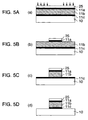
- Figs. 3A-3G illustrate the third embodiment in which address electrodes are formed on the back side substrate.
- This embodiment is the same as that of Fig. 1, except that the blast treatment using calcium carbonate is carried out not only on the inorganic material layer 25 (ITO layer) but also on the Cr layer 11a (Step (d), Fig. 3D), and after etching the Cu layer 11b (Step (e), Fig. 3E) the photoresist 26 (dry film resist) is peeled off (Step (f), Fig. 3F). Accordingly, the photoresist 26 (dry film resist) is selected from materials not etched by the etching solution for Cu layer 11b.
- the step for etching Cr layer 11a can be eliminated, and the electrode-forming process can be simplified. Further, if the efficiencies of blast process and wet etching process are taken into consideration, it is preferable to fabricate down to the Cr layer 11a by blast process because of the material characteristics of Cu layer 11b and film thickness thereof. As above, an electrode formation by combination of a dry etching method such as blast process and a wet etching method is effective for simplification of process and prevention of breakage of wiring.
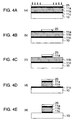
- Figs. 4A-4E illustrate the fourth embodiment in which address electrodes are formed on a back side substrate.
- Fig. 4 is an example of forming electrodes without using photolithographic process.
- Step (a), Fig. 4A Cr layer 11c, Cu layer 11b, Cr layer 11a and ITO layer functioning as an inorganic material layer 25 are successively formed on a glass substrate 10 by sputtering.
- the inorganic material layer 25 (ITO layer) is removed by means of laser so as to give a desired electrode pattern (Step (b), Fig. 4B).
- a resist can be formed by using a laser, without such photolithographic steps as shown in Figs. 1-3, by which the electrode-forming process can be simplified greatly. Further, the mask for forming electrodes becomes unnecessary.
- Cr layer 11c, Cu layer 11b and Cr layer 11a are successively formed on glass substrate 10 by sputtering, after which thereon are formed an ITO layer functioning as inorganic material layer 25 and a resist 27 not corroded by the etching solution for Cu layer 11b (Step (a), Fig. 6A).
- resist 27, inorganic material layer 25 and Cr layer 11a are removed by means of laser so as to give a desired electrode pattern (Step (b), Fig. 6B). Since resist 27 is formed by means of laser as above, there is no need to use such a photosensitive material as used in conventional photolithographic process as a material of resist 27.
- Cu layer 11b is etched in the presence of resist 27 by the use of an aqueous solution containing ferric sulfate and sulfuric acid (Step (c), Fig. 6C). Since the inorganic material layer 25 is covered with resist 27, the inorganic material layer 25 is not readily corroded.
- the resist 27 is peeled off, and the Cr layer 11c is etched with an aqueous solution containing potassium permanganate and sodium metasilicate (Step (d), Fig. 6D). If desired, the resist 27 may be peeled off after Step (e).
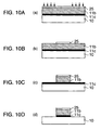
- Figs. 10A to 10D show the seventh embodiment of the present invention wherein the electrode is formed by reducing the number of film formation by sputtering, etc. and aiming at a lower production cost.
- Step (a), Fig. 10A Cr layer 11c, Cu layer 11b and an alloy layer of Ni and Cr as an inorganic material layer 25 are formed on a glass substrate 10 by sputtering (Step (a), Fig. 10A). Since the alloy layer of Ni and Cr is used, selective etching of the Cr layer 11c and Cu layer 11b becomes possible in a later step. Further, the alloy layer of Ni and Cr can easily be subjected to laser processing.
- the inorganic material layer 25 (the alloy layer of Ni and Cr) is removed by using a laser so as to give a desired electrode pattern (Step (b), Fig. 10B). Needless to say, it is possible to employ the above-mentioned blast treatment.
- This electrode construction does not require the Cr layer 11a mentioned in the above-mentioned embodiments, and thus can omit the film forming step of the Cr layer 11a, resulting in making it possible to further reduce the production cost.
- the electrode comprising the Cr layer 11c, the Cu layer 11b and the Ni-Cr alloy layer is effective for preventing wire breaking caused by side etching, as well as for increasing the adhesiveness between the Cr layer 11c and the substrate 10, making the resistance lower by the Cu layer 11b, and preventing the reaction with a dielectric layer (not shown in the drawing) by the Ni-Cr alloy layer, so that requirements demanded for a plasma display panel can be satisfied. It is possible to use SiO 2 , ITO Si, Ni, etc. in place of the Ni-Cr alloy layer.
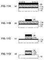
- Figs. 11A to 11D show eighth embodiment of the present invention wherein the electrode is formed by reducing the number of film formation by sputtering, etc. and using a thickened Cr layer as the inorganic material layer 25.
- a Cr layer 11c, a Cu layer 11b and a thick Cr layer which is to become an inorganic material layer 25 are formed in this order by sputtering on a glass substrate 10 (Step (a), Fig. 11A).
- the thickness of the Cr layer 25 is preferably 3 times or more compared with the thickness of the Cr layer 11c, in order to set the process conditions mentioned below easier.
- the thick Cr layer (used as an inorganic material layer 25) is removed using a laser to give a desired electrode pattern (Step (b), Fig. 11B).
- the blast processing can be used as mentioned in the above-mentioned embodiments.
- the Cu layer 11b and the Cr layer 11c are etched in this order in the same manner as shown in Fig. 3 to form an electrode wiring (steps (c) and (d), Figs. 11C and 11D).
- the thick Cr layer (inorganic material layer 25) is also etched to reduce the thickness, but by making the thickness of the thick Cr layer (inorganic material layer 25) sufficiently larger than that of the Cr layer 11c, it is possible to form an electrode having no problem in reliability. Further, by making the thickness of the thick Cr layer larger, pin holes are hardly formed in the thick Cr layer, resulting in reducing the residual amount of an etching solution for the surface of the Cu layer 11b. This makes it possible to prevent corrosion of the Cu layer in later steps due to the remaining etching solution.
- the electrode can be formed by a combination of dry etching such as a conventional layer processing and wet etching.
- Figs. 7A and 7B illustrate a gas discharge display panel, provided that Fig. 7A is a sectional view parallel to address electrodes and Fig. 7B is a sectional view perpendicular to the address electrodes.
- the above-mentioned electrode-forming processes are applied to both of front side substrate and back side substrate.
- 10 is a back side glass substrate
- 11 is an address electrode
- 12 is a thin film dielectric layer such as SiO 2
- 13 is a thick film dielectric layer
- 14 is a front side glass substrate
- 15 is a transparent electrode such as ITO
- 16 is a bus electrode such as Cr-Cu-Cr
- 17 is a thin film dielectric layer such as SiO 2
- 18 is a thick film dielectric layer
- 19 is a protecting film made of, for example, MgO
- 20 is a sealing member
- 21 is an electrode connected from the external circuit
- 22 is an anisotropic conductive sheet containing conductive particles
- 23 is a partition wall
- 24 is a fluorescent material layer
- 25 is an inorganic material layer functioning as a resist at the time of electrode formation.
- a front side substrate can be formed in the following manner.
- a transparent electrode 15 is formed on a glass substrate 14.
- the transparent electrode 15 may be formed by any means of wet etching, blaster and laser. The use of laser is preferred from the viewpoint of simplification of the process.
- a bus electrode 14 is formed on the transparent electrode 15 according to the above-mentioned electrode-forming process of this invention.
- the above-mentioned inorganic material layer 25 exists on the bus electrode 16.
- a thin film dielectric layer 17 is formed so as to cover at least the transparent electrode 15 and the bus electrode 16.
- the thin film dielectric layer 17 is formed on the whole panel surface.
- a thick film dielectric layer 18 is formed on the thin film dielectric layer 17 by the thick film printing technique.
- a protecting film 19 made of MgO or the like is formed on the thick film dielectric layer 18 by the technique of evaporation.
- the transparent electrode 15 is formed under the bus electrode 16, and the transparent electrode 15 is usually an ITO layer. Accordingly, it is allowable, if desired, to form the bus electrode 16 including the transparent electrode 15 and the inorganic material layer 25 according to a series of wet etching processes by applying the electrode-forming process of this invention. In this case, ITO/Cr/Cu/Cr/ITO are successively formed, and then Cr/Cu/Cr/ITO functioning as bus electrode 16 is formed by any of the above-mentioned electrode-forming processes of this invention.
- the inorganic material layer 25 may be made of SiO 2 or Ni-Cr, if desired.
- a back side substrate is formed in the following manner.
- an address electrode 11 is formed on a glass substrate 10 according to the electrode-forming process of this invention.
- a thin film dielectric layer 12 is formed so as to cover at least the address electrode 11.
- the thin film dielectric layer 12 is formed on the whole panel surface.
- a thick film dielectric layer 13 is formed on the thin film dielectric layer 12 according to the thick film printing technique.
- a partition wall 23 is formed and further a fluorescent material layer 24 is formed thereon by the printing technique.
- the partition wall 24 may be formed as stripes parallel to the address electrode or as grids surrounding the display cell.
- the front side substrate and the back side substrate formed above After adjusting the positions of the front side substrate and the back side substrate formed above, they are sealed by means of a sealing member 21.
- the atmosphere of the sealed space contains a rare gas.
- the electrode 21 leading to the external circuit is connected via an external connection terminal of the front side substrate and an anisotropic conductive sheet of the back side substrate, in order to simplify the connecting process.
- the inorganic material layer 25 is free from the risk of reaction with address electrode 11, dielectric layer 18, bus electrode 16 and dielectric layer 13, and therefore the inorganic material layer can be left to remain without peeling. This makes it possible to suppress the reactions between address electrode 11 and dielectric layer 18 and between the bus electrode 16 and the dielectric layer 13, and thereby to prevent the corrosion of address electrode 11 and bus electrode 16. Accordingly, there arises no problem, if the thin film dielectric layer 12 is not formed.
- the bus electrode and address electrode as a Cr/Cu/Cr/ITO layer or a Cr/Cu/Cr/SiO 2 layer, or a Cr/Cu/Cr/Ni-Cr layer, the breakage of wiring due to various causes can be lessened.
- a different resist may be used in either of Cr layer 11a, Cu layer 11b and Cr layer 11c.
- Another allowable means for achieving this object is to form the inorganic material layer into a double layer structure having a constitution of Cr/Cu/Cr/ITO/SiO 2 .
- the same effect as above can be obtained if the Cr/Cu/Cr electrode wiring is replaced by Cr/Al/Cr, Ag, Ni, Au, Al, etc. That is to say, it is needless to say that the same effect as above can be obtained if the materials used therein are those satisfying the conditions required of a gas discharge display panel. It is also needless to say that the electrode to be formed is not restricted to the address electrode but the same effect as above can be obtained by forming the bus electrode of the front side substrate as shown in Fig. 7. Further, it is needless to say that this invention can be applied not only to gas discharge display panel but also to all the wiring substrates in which electrodes are formed by wet etching technique.
- the breakage of wire in the electrodes formed in wiring substrate or gas discharge display device can be suppressed.
- the breakage of wire occurring in the case of forming electrodes by wet etching technique can be suppressed.
Landscapes
- Engineering & Computer Science (AREA)
- Physics & Mathematics (AREA)
- Plasma & Fusion (AREA)
- Manufacturing & Machinery (AREA)
- Chemical & Material Sciences (AREA)
- Materials Engineering (AREA)
- Metallurgy (AREA)
- Microelectronics & Electronic Packaging (AREA)
- Gas-Filled Discharge Tubes (AREA)
- Liquid Crystal (AREA)
- Devices For Indicating Variable Information By Combining Individual Elements (AREA)
Applications Claiming Priority (3)
| Application Number | Priority Date | Filing Date | Title |
|---|---|---|---|
| JP270795/97 | 1997-10-03 | ||
| JP27079597 | 1997-10-03 | ||
| JP27079597 | 1997-10-03 |
Publications (3)
| Publication Number | Publication Date |
|---|---|
| EP0907199A2 true EP0907199A2 (de) | 1999-04-07 |
| EP0907199A3 EP0907199A3 (de) | 2000-03-15 |
| EP0907199B1 EP0907199B1 (de) | 2009-09-02 |
Family
ID=17491123
Family Applications (1)
| Application Number | Title | Priority Date | Filing Date |
|---|---|---|---|
| EP98118551A Expired - Lifetime EP0907199B1 (de) | 1997-10-03 | 1998-10-01 | Verdrahtungssubstrat und Gasentladungs-Anzeigevorrichtung |
Country Status (4)
| Country | Link |
|---|---|
| US (3) | US6261144B1 (de) |
| EP (1) | EP0907199B1 (de) |
| KR (1) | KR100430664B1 (de) |
| DE (1) | DE69841116D1 (de) |
Families Citing this family (20)
| Publication number | Priority date | Publication date | Assignee | Title |
|---|---|---|---|---|
| KR100430664B1 (ko) * | 1997-10-03 | 2004-06-16 | 가부시끼가이샤 히다치 세이사꾸쇼 | 가스방전형표시장치의제조방법 |
| US6555956B1 (en) * | 1998-03-04 | 2003-04-29 | Lg Electronics Inc. | Method for forming electrode in plasma display panel and structure thereof |
| US6355979B2 (en) * | 1999-05-25 | 2002-03-12 | Stmicroelectronics, Inc. | Hard mask for copper plasma etch |
| JP2001015038A (ja) * | 1999-06-30 | 2001-01-19 | Fujitsu Ltd | プラズマディスプレィパネル |
| JP3423261B2 (ja) * | 1999-09-29 | 2003-07-07 | 三洋電機株式会社 | 表示装置 |
| TW525118B (en) * | 2000-05-12 | 2003-03-21 | Acer Display Tech Inc | Plasma display having driving circuit mounted on single face and its manufacturing method |
| TW522435B (en) * | 2000-05-23 | 2003-03-01 | Toray Industries | Slurry, display component and process for producing the display component |
| TWI258317B (en) * | 2002-01-25 | 2006-07-11 | Semiconductor Energy Lab | A display device and method for manufacturing thereof |
| JP3624234B2 (ja) * | 2002-07-17 | 2005-03-02 | パイオニアプラズマディスプレイ株式会社 | プラズマディスプレイパネルの製造装置及びプラズマディスプレイパネルの製造方法 |
| JP2004095349A (ja) * | 2002-08-30 | 2004-03-25 | Fujitsu Hitachi Plasma Display Ltd | プラズマディスプレイパネルの製造方法 |
| KR100499573B1 (ko) * | 2002-12-31 | 2005-07-05 | 엘지.필립스 엘시디 주식회사 | 평판형 형광램프 |
| DE602004030312D1 (de) * | 2003-01-24 | 2011-01-13 | Panasonic Corp | Plasmaanzeigetafel |
| JP4179138B2 (ja) * | 2003-02-20 | 2008-11-12 | 松下電器産業株式会社 | プラズマディスプレイパネル |
| KR100533723B1 (ko) * | 2003-04-25 | 2005-12-06 | 엘지전자 주식회사 | 플라즈마 디스플레이 패널 및 그 제조방법 |
| KR100647590B1 (ko) * | 2003-11-17 | 2006-11-17 | 삼성에스디아이 주식회사 | 플라즈마 디스플레이 패널과, 이의 제조 방법 |
| KR100607968B1 (ko) * | 2004-04-27 | 2006-08-03 | 삼성전자주식회사 | 플라즈마 디스플레이 패널 |
| KR20060012409A (ko) * | 2004-08-03 | 2006-02-08 | 삼성에스디아이 주식회사 | 플라즈마 디스플레이 패널 |
| JP2006134745A (ja) * | 2004-11-08 | 2006-05-25 | Fujitsu Hitachi Plasma Display Ltd | プラズマディスプレイパネルの電極形成方法 |
| JP2007305528A (ja) * | 2006-05-15 | 2007-11-22 | Fujitsu Hitachi Plasma Display Ltd | プラズマディスプレイパネルおよびその製造方法 |
| CN111834233A (zh) * | 2020-06-24 | 2020-10-27 | 南昌欧菲显示科技有限公司 | 线路结构及其制备方法 |
Citations (2)
| Publication number | Priority date | Publication date | Assignee | Title |
|---|---|---|---|---|
| EP0199300A2 (de) | 1985-04-19 | 1986-10-29 | Matsushita Electronics Corporation | Verfahren zum Herstellen eines Musters in einer Metallschicht |
| US5536466A (en) | 1992-04-27 | 1996-07-16 | Futaba Denshi Kogyo Kabushiki Kaisha | Process for manufacturing transparent conductive film wiring board |
Family Cites Families (14)
| Publication number | Priority date | Publication date | Assignee | Title |
|---|---|---|---|---|
| US4454449A (en) * | 1980-06-30 | 1984-06-12 | Ncr Corporation | Protected electrodes for plasma panels |
| US4746219A (en) * | 1986-03-07 | 1988-05-24 | Texas Instruments Incorporated | Local interconnect |
| GB2244860A (en) * | 1990-06-04 | 1991-12-11 | Philips Electronic Associated | Fabricating mim type device array and display devices incorporating such arrays |
| JP3442876B2 (ja) * | 1994-08-31 | 2003-09-02 | パイオニア株式会社 | 交流型プラズマディスプレイ装置 |
| JPH08162009A (ja) | 1994-12-08 | 1996-06-21 | Canon Inc | 電子放出素子および該素子を用いた電子源および画像形成装置ならびにそれらの製造方法 |
| JPH08335439A (ja) | 1995-06-07 | 1996-12-17 | Dainippon Printing Co Ltd | Dc型プラズマディスプレイパネルの陰極及びその形成方法 |
| TW368671B (en) * | 1995-08-30 | 1999-09-01 | Tektronix Inc | Sputter-resistant, low-work-function, conductive coatings for cathode electrodes in DC plasma addressing structure |
| JPH09199039A (ja) * | 1996-01-11 | 1997-07-31 | Hitachi Ltd | ガス放電型表示パネル及びその製造方法 |
| US6001539A (en) * | 1996-04-08 | 1999-12-14 | Lg Electronics, Inc. | Method for manufacturing liquid crystal display |
| KR100268103B1 (ko) * | 1996-10-11 | 2000-10-16 | 윤종용 | 질화크롬을사용한배선및그제조방법,이를이용한액정표시장치및그제조방법 |
| US5939827A (en) * | 1996-12-13 | 1999-08-17 | Tektronix, Inc. | Non-reactive cathode for a PALC display panel using hydrogen-doped helium gas |
| KR100430664B1 (ko) * | 1997-10-03 | 2004-06-16 | 가부시끼가이샤 히다치 세이사꾸쇼 | 가스방전형표시장치의제조방법 |
| KR100265289B1 (ko) * | 1998-01-26 | 2000-09-15 | 윤종용 | 플라즈마식각장치의 캐소우드 제조방법 및 이에 따라 제조되는 캐소우드 |
| US5952781A (en) * | 1998-03-09 | 1999-09-14 | Matsushita Electric Industrial Co., Ltd. | Electrode for high contrast gas discharge panel and the method for manufacturing the same |
-
1998
- 1998-09-30 KR KR10-1998-0040782A patent/KR100430664B1/ko not_active Expired - Fee Related
- 1998-10-01 EP EP98118551A patent/EP0907199B1/de not_active Expired - Lifetime
- 1998-10-01 US US09/164,272 patent/US6261144B1/en not_active Expired - Fee Related
- 1998-10-01 DE DE69841116T patent/DE69841116D1/de not_active Expired - Lifetime
-
2001
- 2001-07-13 US US09/903,495 patent/US6346772B1/en not_active Expired - Fee Related
-
2002
- 2002-02-11 US US10/068,939 patent/US6621217B2/en not_active Expired - Fee Related
Patent Citations (2)
| Publication number | Priority date | Publication date | Assignee | Title |
|---|---|---|---|---|
| EP0199300A2 (de) | 1985-04-19 | 1986-10-29 | Matsushita Electronics Corporation | Verfahren zum Herstellen eines Musters in einer Metallschicht |
| US5536466A (en) | 1992-04-27 | 1996-07-16 | Futaba Denshi Kogyo Kabushiki Kaisha | Process for manufacturing transparent conductive film wiring board |
Also Published As
| Publication number | Publication date |
|---|---|
| US6261144B1 (en) | 2001-07-17 |
| KR100430664B1 (ko) | 2004-06-16 |
| EP0907199A3 (de) | 2000-03-15 |
| US20020014841A1 (en) | 2002-02-07 |
| US6346772B1 (en) | 2002-02-12 |
| US20020070665A1 (en) | 2002-06-13 |
| DE69841116D1 (de) | 2009-10-15 |
| KR19990036713A (ko) | 1999-05-25 |
| EP0907199B1 (de) | 2009-09-02 |
| US6621217B2 (en) | 2003-09-16 |
Similar Documents
| Publication | Publication Date | Title |
|---|---|---|
| EP0907199B1 (de) | Verdrahtungssubstrat und Gasentladungs-Anzeigevorrichtung | |
| US5977708A (en) | Glass material used in, and fabrication method of, a plasma display panel | |
| US5990617A (en) | Plasma display panel and method of forming barrier ribs for the same | |
| JPH1049072A (ja) | ガス放電型表示装置とその製造方法 | |
| US7253560B2 (en) | Triode surface discharge type plasma display panel | |
| KR19990063062A (ko) | 표시관용 양극기판과 그 제조방법 | |
| US4359663A (en) | Gas discharge panel having plurality of shift electrodes | |
| JP4103202B2 (ja) | 配線基板の製造方法 | |
| KR100812221B1 (ko) | 플라스마 디스플레이 패널 및 그 제조 방법 | |
| US6159066A (en) | Glass material used in, and fabrication method of, a plasma display panel | |
| JP3299888B2 (ja) | プラズマディスプレイパネル及びその製造方法 | |
| JP3547461B2 (ja) | プラズマディスプレイパネル及びその製造方法 | |
| JP2993263B2 (ja) | プラズマディスプレイパネル | |
| US20060043876A1 (en) | Self-luminous planar display device and manufacturing method thereof | |
| JPH09274860A (ja) | プラズマディスプレイパネル | |
| JPH10144208A (ja) | 電極の形成方法 | |
| JPH08315733A (ja) | Ac型プラズマディスプレイパネル及びその製造方法 | |
| US20060186814A1 (en) | Electrode terminal part connection structure and plasma display panel having the same | |
| KR19990054298A (ko) | 플라즈마 디스플레이 패널의 제조방법 | |
| JP3334706B2 (ja) | プラズマディスプレイパネルの製造方法 | |
| JPH09283029A (ja) | プラズマディスプレイパネル | |
| KR20020009272A (ko) | 플라즈마 디스플레이 패널 및 그 제조방법 | |
| JPH06139923A (ja) | プラズマディスプレイパネルの製造方法 | |
| JP2000011892A (ja) | ガス放電型表示パネルおよびそれを用いた表示装置 | |
| JP2001319569A (ja) | プラズマディスプレイパネル用基板の製造方法、プラズマディスプレイパネル用基板及びプラズマディスプレイパネル |
Legal Events
| Date | Code | Title | Description |
|---|---|---|---|
| PUAI | Public reference made under article 153(3) epc to a published international application that has entered the european phase |
Free format text: ORIGINAL CODE: 0009012 |
|
| 17P | Request for examination filed |
Effective date: 19981001 |
|
| AK | Designated contracting states |
Kind code of ref document: A2 Designated state(s): DE FR GB NL |
|
| AX | Request for extension of the european patent |
Free format text: AL;LT;LV;MK;RO;SI |
|
| PUAL | Search report despatched |
Free format text: ORIGINAL CODE: 0009013 |
|
| AK | Designated contracting states |
Kind code of ref document: A3 Designated state(s): AT BE CH CY DE DK ES FI FR GB GR IE IT LI LU MC NL PT SE |
|
| AX | Request for extension of the european patent |
Free format text: AL;LT;LV;MK;RO;SI |
|
| AKX | Designation fees paid |
Free format text: DE FR GB NL |
|
| 17Q | First examination report despatched |
Effective date: 20011206 |
|
| GRAP | Despatch of communication of intention to grant a patent |
Free format text: ORIGINAL CODE: EPIDOSNIGR1 |
|
| GRAS | Grant fee paid |
Free format text: ORIGINAL CODE: EPIDOSNIGR3 |
|
| GRAA | (expected) grant |
Free format text: ORIGINAL CODE: 0009210 |
|
| AK | Designated contracting states |
Kind code of ref document: B1 Designated state(s): DE FR GB NL |
|
| REF | Corresponds to: |
Ref document number: 69841116 Country of ref document: DE Date of ref document: 20091015 Kind code of ref document: P |
|
| PLBE | No opposition filed within time limit |
Free format text: ORIGINAL CODE: 0009261 |
|
| STAA | Information on the status of an ep patent application or granted ep patent |
Free format text: STATUS: NO OPPOSITION FILED WITHIN TIME LIMIT |
|
| 26N | No opposition filed |
Effective date: 20100603 |
|
| PGFP | Annual fee paid to national office [announced via postgrant information from national office to epo] |
Ref country code: GB Payment date: 20100929 Year of fee payment: 13 |
|
| PGFP | Annual fee paid to national office [announced via postgrant information from national office to epo] |
Ref country code: NL Payment date: 20101016 Year of fee payment: 13 Ref country code: FR Payment date: 20101020 Year of fee payment: 13 |
|
| PGFP | Annual fee paid to national office [announced via postgrant information from national office to epo] |
Ref country code: DE Payment date: 20100929 Year of fee payment: 13 |
|
| REG | Reference to a national code |
Ref country code: NL Ref legal event code: V1 Effective date: 20120501 |
|
| GBPC | Gb: european patent ceased through non-payment of renewal fee |
Effective date: 20111001 |
|
| REG | Reference to a national code |
Ref country code: FR Ref legal event code: ST Effective date: 20120629 |
|
| PG25 | Lapsed in a contracting state [announced via postgrant information from national office to epo] |
Ref country code: NL Free format text: LAPSE BECAUSE OF NON-PAYMENT OF DUE FEES Effective date: 20120501 Ref country code: DE Free format text: LAPSE BECAUSE OF NON-PAYMENT OF DUE FEES Effective date: 20120501 |
|
| REG | Reference to a national code |
Ref country code: DE Ref legal event code: R119 Ref document number: 69841116 Country of ref document: DE Effective date: 20120501 |
|
| PG25 | Lapsed in a contracting state [announced via postgrant information from national office to epo] |
Ref country code: GB Free format text: LAPSE BECAUSE OF NON-PAYMENT OF DUE FEES Effective date: 20111001 Ref country code: FR Free format text: LAPSE BECAUSE OF NON-PAYMENT OF DUE FEES Effective date: 20111102 |