EP0924768A2 - Halbleiterspeicheranordnung und deren Betriebsverfahren - Google Patents
Halbleiterspeicheranordnung und deren Betriebsverfahren Download PDFInfo
- Publication number
- EP0924768A2 EP0924768A2 EP98123178A EP98123178A EP0924768A2 EP 0924768 A2 EP0924768 A2 EP 0924768A2 EP 98123178 A EP98123178 A EP 98123178A EP 98123178 A EP98123178 A EP 98123178A EP 0924768 A2 EP0924768 A2 EP 0924768A2
- Authority
- EP
- European Patent Office
- Prior art keywords
- memory
- select
- transistor
- voltage
- gate electrode
- Prior art date
- Legal status (The legal status is an assumption and is not a legal conclusion. Google has not performed a legal analysis and makes no representation as to the accuracy of the status listed.)
- Withdrawn
Links
- 239000004065 semiconductor Substances 0.000 title claims abstract description 209
- 238000000034 method Methods 0.000 title claims description 98
- 238000009792 diffusion process Methods 0.000 claims abstract description 207
- 230000005641 tunneling Effects 0.000 claims abstract description 55
- 239000000758 substrate Substances 0.000 claims abstract description 48
- 230000005684 electric field Effects 0.000 claims description 7
- 239000012212 insulator Substances 0.000 claims description 7
- 239000004020 conductor Substances 0.000 claims 2
- 239000012535 impurity Substances 0.000 claims 2
- 230000006872 improvement Effects 0.000 abstract description 4
- 238000002347 injection Methods 0.000 abstract 1
- 239000007924 injection Substances 0.000 abstract 1
- 239000010410 layer Substances 0.000 description 139
- 238000010586 diagram Methods 0.000 description 50
- 230000015556 catabolic process Effects 0.000 description 27
- 230000008901 benefit Effects 0.000 description 10
- 230000006866 deterioration Effects 0.000 description 10
- 229910021420 polycrystalline silicon Inorganic materials 0.000 description 9
- 229920005591 polysilicon Polymers 0.000 description 9
- 238000005516 engineering process Methods 0.000 description 7
- 230000000694 effects Effects 0.000 description 6
- 230000008569 process Effects 0.000 description 6
- 238000009826 distribution Methods 0.000 description 5
- 230000001747 exhibiting effect Effects 0.000 description 5
- 238000004519 manufacturing process Methods 0.000 description 5
- 230000002411 adverse Effects 0.000 description 4
- 230000007423 decrease Effects 0.000 description 4
- 239000002019 doping agent Substances 0.000 description 4
- 230000009467 reduction Effects 0.000 description 3
- 230000004913 activation Effects 0.000 description 2
- 230000002542 deteriorative effect Effects 0.000 description 2
- 230000006870 function Effects 0.000 description 2
- 239000002184 metal Substances 0.000 description 2
- 229910052751 metal Inorganic materials 0.000 description 2
- 230000002093 peripheral effect Effects 0.000 description 2
- 230000003247 decreasing effect Effects 0.000 description 1
- 239000002784 hot electron Substances 0.000 description 1
- 238000009413 insulation Methods 0.000 description 1
- 238000002955 isolation Methods 0.000 description 1
- 230000003647 oxidation Effects 0.000 description 1
- 238000007254 oxidation reaction Methods 0.000 description 1
- 229910052710 silicon Inorganic materials 0.000 description 1
- 239000010703 silicon Substances 0.000 description 1
- 239000002356 single layer Substances 0.000 description 1
Images











Classifications
-
- G—PHYSICS
- G11—INFORMATION STORAGE
- G11C—STATIC STORES
- G11C16/00—Erasable programmable read-only memories
- G11C16/02—Erasable programmable read-only memories electrically programmable
- G11C16/04—Erasable programmable read-only memories electrically programmable using variable threshold transistors, e.g. FAMOS
- G11C16/0408—Erasable programmable read-only memories electrically programmable using variable threshold transistors, e.g. FAMOS comprising cells containing floating gate transistors
- G11C16/0416—Erasable programmable read-only memories electrically programmable using variable threshold transistors, e.g. FAMOS comprising cells containing floating gate transistors comprising cells containing a single floating gate transistor and no select transistor, e.g. UV EPROM
-
- G—PHYSICS
- G11—INFORMATION STORAGE
- G11C—STATIC STORES
- G11C16/00—Erasable programmable read-only memories
- G11C16/02—Erasable programmable read-only memories electrically programmable
- G11C16/04—Erasable programmable read-only memories electrically programmable using variable threshold transistors, e.g. FAMOS
- G11C16/0408—Erasable programmable read-only memories electrically programmable using variable threshold transistors, e.g. FAMOS comprising cells containing floating gate transistors
- G11C16/0433—Erasable programmable read-only memories electrically programmable using variable threshold transistors, e.g. FAMOS comprising cells containing floating gate transistors comprising cells containing a single floating gate transistor and one or more separate select transistors
-
- H—ELECTRICITY
- H10—SEMICONDUCTOR DEVICES; ELECTRIC SOLID-STATE DEVICES NOT OTHERWISE PROVIDED FOR
- H10B—ELECTRONIC MEMORY DEVICES
- H10B69/00—Erasable-and-programmable ROM [EPROM] devices not provided for in groups H10B41/00 - H10B63/00, e.g. ultraviolet erasable-and-programmable ROM [UVEPROM] devices
Definitions
- the present invention relates to a nonvolatile semiconductor memory device and a method for driving the same. More particularly, the present invention relates to a nonvolatile semiconductor memory device functioning as a flash EEPROM employing a two-layer gate electrode structure including floating gate and control gate electrodes and to a method for driving the same.
- a flash EEPROM is increasingly required to perform a rewrite operation using a single power supply at a low voltage and a high-speed read operation at a low voltage.
- a "low voltage” herein refers to about 1.5 V to about 3.3 V.
- a flash EEPROM developed by a certain corporation injects channel hot electrons (CHE) from a drain into a floating gate electrode while writing, and ejects the electrons out of the electrode into a source by using FN tunneling current while erasing.
- CHE-type flash EEPROM a flash EEPROM of this type will be called a "CHE-type flash EEPROM”.
- the CHE-type flash EEPROM is advantageous in that the circuit configuration and fabrication process thereof can be implemented by extending EPROM technologies.
- current of about 500 ⁇ A should be consumed per cell for writing, a rewrite operation using a single power supply at 5 V can be performed relatively easily. But a rewrite operation using a single power supply at 2.5 V or less is hard to realize.
- flash EEPROM ejecting electrons out of a floating gate electrode into a drain while writing and injecting electrons into the floating gate electrode while erasing by using, in both operations, FN tunneling current over the entire surface of a channel.
- flash EEPROMs of this type include a DINOR-type flash EEPROM disclosed in United States Patent No. 5,283,758 and an AND-type flash EEPROM disclosed in United States Patent No. 5,592,415. Flash EEPROMs of those types use the FN tunneling current for both writing and erasing.
- the level of current required for writing and erasing may be low and therefore a rewrite operation can be performed using a single power supply at a low voltage (e.g., 2.5 V).
- a flash EEPROM of such a type will be called a "drain-side FN-FN type flash EEPROM".
- a memory cell structure for a drain-side FN-FN type flash EEPROM and a method for driving the same will be described, and the problems thereof will be clarified. And then another conventional nonvolatile semiconductor memory device and a method for driving the same will be described as an exemplary means for solving the problems. It is noted that the drain-side FN-FN type flash EEPROM exemplified below is supposed to be a DINOR-type flash EEPROM.
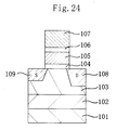
- Figure 24 is a cross-sectional view illustrating an exemplary memory cell structure for a drain-side FN-FN type flash EEPROM.
- the memory cell includes: a P-type semiconductor substrate 101 ; a deep N-type well 102 ; a P-type well 103 ; a gate insulating film 104 ; a floating gate electrode 105 ; an interelectrode insulating film 106 ; a control gate electrode 107 ; a drain diffusion layer 108 ; and a source diffusion layer 109 .
- the flash EEPROM shown in Figure 24 has fundamentally the same memory cell structure as that of the CHE-type flash EEPROM, but is somewhat different from the latter in the shapes of the diffusion layers. Specifically, in a memory cell of the CHE-type flash EEPROM, a source diffusion layer is deeper than a drain diffusion layer. Conversely, in a memory cell of the drain-side FN-FN type flash EEPROM, the drain diffusion layer 108 is deeper than the source diffusion layer 109 . This structural difference comes from the locations of the tunneling current utilized by the flash EEPROMs of these two types.
- the CHE-type flash EEPROM uses the tunneling current flowing between the source diffusion layer and the floating gate electrode
- the drain-side FN-FN type flash EEPROM uses the tunneling current flowing between the drain diffusion layer 108 and the floating gate electrode 105 .
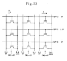
- Figure 25(a) is an electric circuit diagram illustrating voltages applied for simultaneously erasing data from all the memory cells in the drain-side FN-FN type flash EEPROM as a conventional nonvolatile semiconductor memory device.
- Figure 25(b) is a cross-sectional view illustrating how electrons move during the erase operation.
- each memory word line M.W-0 , 1 , 2 interconnects the control gate electrodes 107 of memory cells arranged on the same row in the direction X .
- Each source line S-0 , 1 , 2 interconnects the source diffusion layers 109 of memory cells arranged on the same row in the direction X .
- each bit line B-0 , 1 , 2 interconnects the drain diffusion layers 108 of memory cells arranged on the same column in the direction Y .
- the source lines are disposed in parallel to the word lines for memory cells (i.e., the memory word lines) and the bit lines are disposed vertically to the memory word lines.
- Figure 25(a) illustrates the voltages applied for simultaneously erasing data from all of the nine memory cells illustrated.
- a voltage of +7 V is applied to the memory word lines M.W-0 , 1 , 2 and a voltage of -7 V is applied to the P-type well PW .
- the potential difference between the control gate electrode 107 and the surface of the channel is 14 V at every memory transistor. Consequently, as shown in Figure 25(b) , tunneling current flows from the entire surface region of the channel into the floating gate electrode 105 , whereby electrons are injected into the floating gate electrode 105 .
- the threshold voltage of the memory transistor is about 4 V.
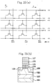
- Figure 26(a) is an electric circuit diagram illustrating voltages applied for writing data into only one memory cell located at the center of the array and selected from the nine memory cells included in the drain-side FN-FN type flash EEPROM.
- Figure 26(b) is a cross-sectional view illustrating how electrons move during the write operation.
- a voltage of -9 V is applied to the memory word line M.W-1 connected to the memory cell to which data is selectively written (i.e., a selected memory cell).
- voltages of +5 V and 0 V are respectively applied to the bit line B-1 connected to the selected memory cell and to the P-type well ( PW ) 3 .
- the potential difference between the control gate electrode 107 and the drain diffusion layer 108 is 14 V at the selected memory cell. Consequently, as shown in Figure 26(b) , tunneling current flows from the floating gate electrode 105 into the drain diffusion layer 108 and electrons are ejected out of the floating gate electrode 105 .
- the threshold voltage of the memory transistor is about 1.2 V.
- a voltage of 0 V is applied to the other memory word lines M.W-0 , 2 and to the other bit lines B-0 , 2 .
- the potential difference between the control gate electrode 107 and the drain diffusion layer 108 can be no greater than 9 V at the non-selected memory cells and it is possible to prevent the data from being erroneously written into the non-selected memory cells.
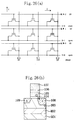
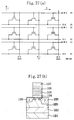
- Figure 27(a) is an electric circuit diagram illustrating voltages applied for reading data from only one memory cell located at the center and selected from the nine memory cells included in the drain-side FN-FN type flash EEPROM as a nonvolatile semiconductor memory device.
- Figure 27(b) is a cross-sectional view illustrating how electrons move during the read operation.
- a voltage of 3 V is applied to the memory word line M.W-1 connected to a memory cell from which data is selectively read out (i.e., a selected memory cell).
- voltages of 1 V and 0 V are respectively applied to the bit line B-1 connected to the selected memory cell and the P-type well PW .
- the drain-side FN-FN type flash EEPROM has the following three problems.
- the first problem concerns the unsatisfactory reliability thereof.
- a potential difference of about 5 V is required between the drain diffusion layer 108 and the P-type well 103 .
- band-to-band tunneling current is generated between the drain diffusion layer 108 and the P-type well 103 .
- holes are generated owing to the band-to-band tunneling current in the vicinity of a boundary region between the P-type well 103 and the drain diffusion layer 108 , and are trapped in the gate insulating film 104 . Consequently, the reliability is deteriorated.
- the second problem pertains to the power consumed during writing.
- the band-to-band tunneling current is generated as described above. Accordingly, write current of about 100 nA is required per cell.
- a memory cell of the drain-side FN-FN type flash EEPROM is constituted by only one memory transistor. Accordingly, if the variation in threshold voltages is to be controlled after the write operation has been performed, then a write depth (i.e., the threshold voltage) should be controlled on a bit-by-bit basis, which requires a too much complicated controller. Moreover, since the controllable variation of the threshold voltage is as small as about 0.8 V, the threshold voltages after the write operation has been performed are distributed in the range from about 0.8 V to about 1.6 V. Thus, in order not to cause erroneous reading, the power supply voltage cannot be less than about 2.5 V, even through the voltage is preferably further lower.
- nonvolatile semiconductor memory device in which a memory cell includes a side-wall-shaped select transistor, was proposed in United States Patent No. 5,402,371, for example.
- the nonvolatile semiconductor memory device and a method for driving the same will be described.
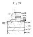
- Figure 28 is a cross-sectional view illustrating a memory cell structure for the nonvolatile semiconductor memory device.
- a select transistor is formed as a sidewall on the side face of the floating gate electrode 105 and the control gate electrode 107 , and includes a select gate electrode 113 .
- a lateral interelectrode insulating film 112 is interposed between the select gate electrode 113 and the floating gate and control gate electrodes 105 , 107 .
- a gate insulating film 111 is interposed between the select gate electrode 113 and the substrate.
- the memory cell shown in Figure 28 uses the sidewall-shaped select gate electrode 113 made of polysilicon, thereby realizing a rewrite operation using the tunneling current flowing between the floating gate electrode 105 and the entire surface of the channel for both writing and erasing.
- no potential difference is required between the drain diffusion layer 108 and the P-type well 103 , and therefore no band-to-band tunneling current is generated. Accordingly, no holes resulting from the band-to-band tunneling current are generated.
- the reliability problem can be solved and the current consumed during rewriting can be reduced.
- the threshold voltage of a memory transistor may be determined by the threshold voltage of the select transistor additionally provided.
- Such a rewrite method using the tunneling current flowing between the floating gate electrode 105 and the entire surface of the channel for both writing and erasing was also implemented by a NAND-type flash EEPROM. Also, it was already proved that this method is more advantageous in terms of reliability (i.e., the number of times satisfactory rewriting is ensured). In addition, this method enables a rewrite operation using a single power supply at a lower voltage.
- the NAND-type flash EEPROM has an array structure of a NAND type, this flash EEPROM requires an adversely long random access time.
- the non-volatile semiconductor memory device shown in Figure 28 has an array structure of a NOR type, and therefore can effectively perform random access in a shorter time. However, the cell size of the NOR-type flash EEPROM is larger than that of the NAND-type flash EEPROM.
- the nonvolatile semiconductor memory device shown in Figure 28 has a NOR-type array structure enabling random access at a higher speed and realizes a rewrite operation using the tunneling current between the floating gate electrode 105 and the entire surface of the channel for both writing and erasing.
- the array structure of the conventional nonvolatile semiconductor memory device shown in Figure 28 and a method for driving the same will be described.
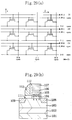
- Figure 29(a) is an electric circuit diagram illustrating voltages applied for simultaneously erasing data from all the memory cells, each including the sidewall-shaped select transistor of the conventional nonvolatile semiconductor memory device as shown in Figure 28 .
- Figure 29(b) is a cross-sectional view illustrating how electrons move during the erase operation.
- each memory word line M.W-0 , 1 , 2 interconnects the control gate electrodes 107 of memory cells arranged on the same row in the direction X .
- Each select word line S.W-0 , 1 , 2 interconnects the select gate electrodes 113 of memory cells arranged on the same row in the direction X .
- Each source line S-0 , 1 , 2 interconnects the source diffusion layers 109 of memory cells arranged on the same row in the direction X .
- each bit line B-0 , 1 , 2 interconnects the drain diffusion layers 108 of memory cells arranged on the same column in the direction Y .
- the source lines are disposed in parallel to the word lines for memory cells (i.e., the memory word lines and the select word lines) and the bit lines are disposed vertically to the word lines.
- Figure 29(a) illustrates the voltages applied for simultaneously erasing data from all of the nine memory cells illustrated.
- a voltage of -7 V is applied to the memory word lines M.W-0 , 1 and 2 and a voltage of +7 V is applied to the P-type well PW .
- the potential difference between the control gate electrode 107 and the surface of the channel is 14 V at every memory transistor.
- tunneling current flows from the floating gate electrode 105 into the entire surface region of the channel, whereby electrons are ejected out of the floating gate electrode 105 .
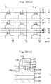
- Figure 30(a) is an electric circuit diagram illustrating voltages applied for writing data into only one memory cell located at the center and selected from the nine memory cells, each including the sidewall-shaped select transistor of the nonvolatile semiconductor memory device as shown in Figure 28 .
- Figure 30(b) is a cross-sectional view illustrating how electrons move during the write operation.
- a voltage of +9 V is applied to the memory word line M.W-1 connected to a memory cell to which data is selectively written (i.e., a selected memory cell).
- a voltage of -5 V is applied to the select word line S.W-1 and the bit line B-1 that are connected to the selected memory cell and to the P-type well PW .
- the potential difference between the control gate electrode 107 and the surface region of the channel is 14 V at the selected memory transistor. Accordingly, as shown in Figure 30(b) , tunneling current flows from the entire surface region of the channel into the floating gate electrode 105 , whereby electrons are injected into the floating gate electrode 105 .
- a voltage of -5 V is applied to the other memory word lines M.W-0 , 2 and select word lines S.W-0 , 2 , and a voltage of 0 V is applied to the other bit lines B-0, 2 .
- the potential difference between the control gate electrode 107 and the surface region of the channel can be no greater than 9 V at the non-selected memory cells and it is possible to prevent the data from being erroneously written into the non-selected memory cells.
- a voltage of -5 V is applied to all the select word lines S.W-0 , 1 , 2 , because all the select transistors should be turned OFF.
- Figure 31(a) is an electric circuit diagram illustrating voltages applied for reading data from only one memory cell located at the center and selected from the nine memory cells, each including the sidewall-shaped select transistor of the nonvolatile semiconductor memory device as shown in Figure 28 .
- Figure 31(b) is a cross-sectional view illustrating how electrons move during the read operation. As shown in Figure 31(a) , a voltage of 3 V is applied to the memory word line M.W-1 connected to the memory cell from which data is selectively read out (i.e., a selected memory cell).
- the nonvolatile semiconductor memory device shown in Figure 28 and the method for driving the same have the following three advantages over the drain-side FN-FN type flash EEPROM shown in Figure 24 .
- the first advantage lies in the improvement of reliability.
- a potential difference of about 5 V is required between the drain diffusion layer 108 and the P-type well 103 .
- a voltage of -9 V is applied to the control gate electrode 107 , band-to-band tunneling current is generated.
- holes are generated owing to the band-to-band tunneling current and trapped in the gate insulating film 104 . Consequently, the reliability is deteriorated.
- the flash EEPROM shown in Figure 28 including the sidewall-shaped select gate electrode uses the tunneling current flowing between the floating gate electrode 105 and the entire surface region of the channel of the memory transistor for both writing and erasing. Accordingly, no potential difference is generated between the drain diffusion layer 108 and the P-type well 103 and no band-to-band tunneling current is generated. Thus, since almost no holes are generated, the deterioration of reliability can be suppressed.
- the second advantage pertains to the reduction of power consumed during writing and erasing.
- the band-to-band tunneling current is generated as described above. Accordingly, write current of about 100 nA is required per memory cell.
- the flash EEPROM shown in Figure 28 no band-to-band tunneling current is generated during either writing or erasing. Thus, write current of only 1 nA or less is required per memory cell.
- the flash EEPROM shown in Figure 28 can operate while consuming one-hundredth or less power compared with the drain-side FN-FN type flash EEPROM. As a result, the area occupied by an internal voltage step-up circuit can be reduced. Alternatively, since the number of bits, to which data can be written simultaneously, increases, a write time can be decreased or a rewrite operation can be performed at an even lower voltage.
- the third advantage relates to the lower limit of the power supply voltage during reading.
- a memory cell of the drain-side FN-FN type flash EEPROM is constituted by only one memory transistor. Accordingly, if the variation in threshold voltages is to be controlled after the write operation has been performed, then a write depth (i.e., the threshold voltage) should be controlled on a bit-by-bit basis, which requires a too much complicated controller. Moreover, since the controllable variation of the threshold voltages is as small as about 0.8 V, the threshold voltages after the write operation has been performed are distributed within a range from about 0.8 V to about 1.6 V. Thus, in order not to cause erroneous reading, the power supply voltage cannot be less than about 2.5 V, even through the voltage is preferably further lower.
- a memory cell has a serial connection of two transistors, i.e., select transistor and memory transistor. Accordingly, even when the threshold voltage of the memory transistor is negative, the threshold voltage of the memory cell is no lower than the threshold voltage of the select transistor.
- the threshold voltage of the memory cell can be set somewhere between about 0.6 V and about 0.8 V. By narrowing the voltage range in this manner, reading can be performed at as low as about 1.5 V, for example.
- the area occupied by a memory cell increases.
- a memory cell is constituted by a single memory transistor.
- the memory cell structure of the flash EEPROM shown in Figure 28 requires a select transistor to operate, the area occupied by a memory cell increases for that part.
- the increase of the area occupied by a single memory cell is less large than the case of additionally providing a select transistor for the drain-side FN-FN type flash EEPROM.
- the nonvolatile semiconductor memory device shown in Figure 28 and a method for driving the same can be regarded as having the above described three advantages over the drain-side FN-FN type flash EEPROM.
- the following two problems are likely to be caused.
- the first problem concerns the reliability of the lateral interelectrode insulating film 112 formed between the select gate electrode and the control gate electrode.
- the lateral thickness (i.e., the gate length) of the select gate electrode 113 shaped like a sidewall cannot be too large and at most about 0.2 ⁇ m in view of the process efficiency. Accordingly, the thickness of the gate insulating film 111 of the select transistor should be about 4 nm or more to make the select transistor exert its originally intended function.
- the thickness of the lateral interelectrode insulating film 112 is at most about 10 nm even when the effect of accelerated oxidation of polysilicon is taken into consideration. That is to say, since a potential difference of 14 V is generated in the lateral interelectrode insulating film 112 having a thickness as small as 10 nm during writing, insulation breakdown possibly happens to deteriorate the reliability.
- the second problem relates to the source-to-drain breakdown voltage of the select transistor including the select gate electrode 113 .
- the drain diffusion layer 108 of the select transistor in each of the non-selected memory cells connected in common with the selected memory cell to the same word line has a potential of about 0 V.
- the source diffusion layer 109 thereof has a potential of about -5 V.
- the potential of the source diffusion layer 109 is substantially equal to that of the P-type well.
- a potential difference of about 5 V is generated between the drain diffusion layer 108 and the source diffusion layer 109 .
- the gate length of the select gate electrode 113 is at most about 0.2 ⁇ m
- the source-to-drain breakdown voltage of the select transistor is at most about 2.5 V, which is far lower than 5 V. Accordingly, during writing, since the select transistors of the non-selected memory cells are not turned OFF, erroneous writing possibly happens.
- the object of the present invention is to provide a non-volatile semiconductor memory device functioning as a flash EEPROM, in which a memory cell includes a memory transistor and a select transistor, and a method for driving the same.
- the device of the present invention is configured to prevent the lateral interelectrode insulating film between the select transistor and the memory transistor from being deteriorated and to suppress erroneous writing resulting from an insufficient source-to-drain breakdown voltage of the select transistor.
- the present invention takes the measures of: using an independent transistor, not a sidewall-shaped transistor, as the select transistor; disposing electrically independent source lines in parallel to or vertically to respective bit lines (i.e., vertically to or in parallel to respective word lines); and providing a plurality of electrically independent well regions for the respective bit lines.
- a first nonvolatile semiconductor memory device has an array of memory cells arranged in columns and rows over a well region of a semiconductor substrate.
- Each of the memory cells includes a memory transistor including: a first gate insulating film, which is formed on the semiconductor substrate and has such a thickness as to allow tunneling current to pass therethrough; a floating gate electrode, which is formed on the first gate insulating film and where charges are storable; an interelectrode insulating film formed on the floating gate electrode; and a control gate electrode formed on the interelectrode insulating film.
- Each memory cell further includes: a select transistor including a second gate insulating film formed on the semiconductor substrate and a select gate electrode formed on the second gate insulating film, the select transistor being disposed on the semiconductor substrate to be spaced apart from the memory transistor; an intermediate diffusion layer formed in a region of the semiconductor substrate and located between the memory transistor and the select transistor; and source/drain diffusion layers formed in the semiconductor substrate to interpose a region underlying the memory transistor, a region underlying the select transistor and the intermediate diffusion layer therebetween.
- the first device of the present invention has such a structure as preventing band-to-band tunneling current from being generated, the reliability can be improved and the power consumption during writing and erasing can be reduced.
- this device since this device includes a select transistor, the threshold voltage of a memory cell can be defined by the stable threshold voltage of the select transistor. Accordingly, the power supply voltage may be low during reading.
- the memory transistor and the select transistor are provided to be spaced apart from each other. Thus, unlike a conventional nonvolatile semiconductor memory device where a memory cell includes a sidewall-shaped select gate electrode, the deterioration in reliability of a lateral interelectrode insulating film is not an issue in this device of the present invention.
- the gate length of the select gate electrode of the select transistor can be set at a sufficiently large value. Accordingly, the breakdown voltage of the select transistor is no longer insufficient. Consequently, a nonvolatile semiconductor memory device, exhibiting excellent characteristics and having an easily implementable structure, is realized.
- the select transistor may be disposed between the source diffusion layer and the intermediate diffusion layer, while the memory transistor may be disposed between the drain diffusion layer and the intermediate diffusion layer.
- the first device may further include: a plurality of memory word lines, each said memory word line interconnecting the control gate electrodes of the respective memory transistors in the memory cells arranged on the same row and associated with the memory word line; a plurality of select word lines, each said select word line interconnecting the select gate electrodes of the respective select transistors in the memory cells arranged on the same row and associated with the select word line; a plurality of source lines, each said source line interconnecting the source diffusion layers of the memory cells arranged on the same row and associated with the source line; and a plurality of bit lines, each said bit line interconnecting the drain diffusion layers of the memory cells arranged on the same column and associated with the bit line.
- the select transistor is preferably disposed between the source diffusion layer and the intermediate diffusion layer, while the memory transistor is preferably disposed between the drain diffusion layer and the intermediate diffusion layer.
- the first device preferably further includes: a plurality of memory word lines, each said memory word line interconnecting the control gate electrodes of the respective memory transistors in the memory cells arranged on the same row and associated with the memory word line; a plurality of select word lines, each said select word line interconnecting the select gate electrodes of the respective select transistors in the memory cells arranged on the same row and associated with the select word line; a plurality of source lines, each said source line interconnecting the source diffusion layers of the memory cells arranged on the same column and associated with the source line; and a plurality of bit lines, each said bit line interconnecting the drain diffusion layers of the memory cells arranged on the same column and associated with the bit line.
- the source lines extend in parallel to the bit lines (i.e., along the columns) and are provided electrically independently from each other for the respective bit lines. Accordingly, in this structure, no leakage current is generated between bit lines through a source line. As a result, not only the above effects are attained, but also erroneous writing can be prevented without fail while electrons are injected into the floating gate electrode of the memory transistor. Moreover, the circuit size of a decoder controlling a select word line can be reduced and a high-speed operation is realized.
- the select transistor may be disposed between the drain diffusion layer and the intermediate diffusion layer, while the memory transistor may be disposed between the source diffusion layer and the intermediate diffusion layer.
- the first device may further include: a plurality of memory word lines, each said memory word line interconnecting the control gate electrodes of the respective memory transistors in the memory cells arranged on the same row and associated with the memory word line; a plurality of select word lines, each said select word line interconnecting the select gate electrodes of the respective select transistors in the memory cells arranged on the same row and associated with the select word line; a plurality of source lines, each said source line interconnecting the source diffusion layers of the memory cells arranged on the same column and associated with the source line; and a plurality of bit lines, each said bit line interconnecting the drain diffusion layers of the memory cells arranged on the same column and associated with the bit line.
- the source lines extend in parallel to the bit lines (i.e., along the columns) and are provided electrically independently for the respective bit lines, the effects described above can be attained.
- the configuration of a bit line driver including a read circuit can be simplified, this structure is advantageous to a high-speed read operation.
- the well region is divided into a plurality of electrically isolated regions corresponding to the respective columns.
- the potential in each well region can be controlled on a bit line basis.
- the potential difference between a source or drain diffusion layer and an associated well region can be 0 V and no breakdown voltage needs to be secured for this part.
- the reliability can be further improved.
- the select transistor may be disposed between the source diffusion layer and the intermediate diffusion layer, while the memory transistor may be disposed between the drain diffusion layer and the intermediate diffusion layer.
- the first device may further include: a plurality of memory word lines, each said memory word line interconnecting the control gate electrodes of the respective memory transistors in the memory cells arranged on the same row and associated with the memory word line; a plurality of select word lines, each said select word line interconnecting the select gate electrodes of the respective select transistors in the memory cells arranged on the same row and associated with the select word line; a plurality of source lines, each said source line interconnecting the source diffusion layers of the memory cells arranged on the same column and associated with the source line; and a plurality of bit lines, each said bit line interconnecting the drain diffusion layers of the memory cells arranged on the same column and associated with the bit line.
- the select transistor is preferably disposed between the drain diffusion layer and the intermediate diffusion layer, while the memory transistor is preferably disposed between the source diffusion layer and the intermediate diffusion layer.
- the first device preferably further includes: a plurality of memory word lines, each said memory word line interconnecting the control gate electrodes of the respective memory transistors in the memory cells arranged on the same row and associated with the memory word line; a plurality of select word lines, each said select word line interconnecting the select gate electrodes of the respective select transistors in the memory cells arranged on the same row and associated with the select word line; a plurality of source lines, each said source line interconnecting the source diffusion layers of the memory cells arranged on the same column and associated with the source line; and a plurality of bit lines, each said bit line interconnecting the drain diffusion layers of the memory cells arranged on the same column and associated with the bit line.
- the source lines are provided in parallel to the bit lines and electrically independently from each other for the respective bit lines. Accordingly, in this structure, no leakage current is generated between bit lines through a source line. As a result, erroneous writing can be prevented without fail while electrons are injected into the floating gate electrode of the memory transistor.
- the first device may further include a circuit for controlling a potential in each said select word line, the circuit being a high-power transistor optimized to operate at about a power supply voltage such that the potential in the select word line is variable in the range from a ground potential to the power supply voltage.
- the circuit size of a decoder can be reduced and a high-speed read operation is realized.
- the first device may further include a circuit for controlling a potential in each said bit line, the circuit being a high-power transistor optimized to operate at about a power supply voltage such that the potential in the bit line is variable in the range from a ground potential to the power supply voltage.
- the second gate insulating film of the select transistor and the first gate insulating film of the memory transistor are formed at the same thickness during the same process step such that a potential difference between the select gate electrode of the select transistor and the well region causes an electric field of 5 MV/cm or less to be applied to the second gate insulating film.
- the thickness of the second gate insulating film may be adjusted at such a value as limiting the voltage applied thereto to 5 V or less, while the thickness of the first gate insulating film may be adjusted at such a value as allowing electrons to be tunneled.
- a second nonvolatile semiconductor memory device has an array of memory cells arranged in columns and rows over a well region of a semiconductor substrate.
- Each memory cell includes a memory transistor including: a first gate insulating film, which is formed on the semiconductor substrate and has such a thickness as to allow tunneling current to pass therethrough; a floating gate electrode, which is formed on the first gate insulating film and where charges are storable; an interelectrode insulating film formed on the floating gate electrode; and a control gate electrode formed on the interelectrode insulating film.
- Each memory cell further includes source/drain diffusion layers formed in the semiconductor substrate to interpose a region underlying the memory transistor therebetween. The well region is divided into a plurality of electrically isolated regions corresponding to the respective columns.
- the second device Since the second device has a structure making the potential in a well region controllable on a bit line basis, the potential difference between a source or drain diffusion layer and an associated well region can be 0 V and no breakdown voltage needs to be secured for this part. As a result, satisfactory reliability can be ensured without providing a select transistor, and therefore the device size can be further miniaturized while attaining the above effects.
- the second device preferably further includes: a plurality of memory word lines, each said memory word line interconnecting the control gate electrodes of the respective memory transistors in the memory cells arranged on the same row and associated with the memory word line; a plurality of source lines, each said source line interconnecting the source diffusion layers of the memory cells arranged on the same column and associated with the source line; and a plurality of bit lines, each said bit line interconnecting the drain diffusion layers of the memory cells arranged on the same column and associated with the bit line.
- the first or second device may further include: a plurality of laterally isolating regions, formed along the columns and between the respective well regions and made of a semiconductor or an insulator of an opposite conductivity type to that of the well regions, for laterally isolating the respective well regions from each other; and a plurality of vertically isolating regions, each said vertically isolating region being interposed between an associated one of the well regions and the semiconductor substrate and made of a semiconductor or an insulator of the opposite conductivity type to that of the well regions.
- the well regions can be electrically isolated from each other for the respective columns with more certainty.
- a first method for driving a nonvolatile semiconductor memory device is a method for driving the first nonvolatile semiconductor memory device.
- tunneling current allowing electrons to pass through the first gate insulating film of the memory transistor, is used while the electrons are ejected out of the floating gate electrode and while the electrons are injected into the floating gate electrode.
- a nonvolatile semiconductor memory device having such a structure as preventing the deterioration in reliability of the lateral interelectrode insulating film and the shortage of a breakdown voltage unlike a conventional nonvolatile semiconductor memory device, is driven so as to prevent band-to-band tunneling current from being generated. Accordingly, write and erase operations can be performed with low power consumption while suppressing the deterioration in characteristics of the nonvolatile semiconductor memory device.
- an erase operation is performed by applying a ground potential or a first negative voltage to the control gate electrode of the memory transistor and a second voltage, higher than the first voltage, to the well region and thereby ejecting electrons out of the floating gate electrode of the memory transistor.
- tunneling current flows through the entire surface of the first gate insulating film and electrons move from the floating gate electrode toward the well region.
- the band-to-band tunneling current is not generated, and therefore an erase operation can be performed with low power consumption and without deteriorating the reliability.
- a threshold voltage of the memory transistor is negative after the erase operation has been performed.
- the threshold voltage of the select transistor if the threshold voltage of the select transistor is set at a relatively low positive voltage, the threshold voltage of a memory cell can be easily defined by the threshold voltage of the select transistor, even through the threshold voltage of the memory transistor is variable. Accordingly, a read operation can be performed at a low voltage.
- the select transistor may be disposed between the source diffusion layer and the intermediate diffusion layer, while the memory transistor may be disposed between the drain diffusion layer and the intermediate diffusion layer.
- the device may further include: a plurality of memory word lines, each said memory word line interconnecting the control gate electrodes of the respective memory transistors in the memory cells arranged on the same row and associated with the memory word line; a plurality of select word lines, each said select word line interconnecting the select gate electrodes of the respective select transistors in the memory cells arranged on the same row and associated with the select word line; a plurality of source lines, each said source line interconnecting the source diffusion layers of the memory cells arranged on the same row or the same column and associated with the source line; and a plurality of bit lines, each said bit line interconnecting the drain diffusion layers of the memory cells arranged on the same column and associated with the bit line.
- a write operation may be performed by applying: a first positive voltage to the control gate electrode of one of the memory transistors, to which transistor data is written; a second voltage, lower than the first voltage, to the control gate electrodes of the other memory transistors, to which the data is not written; a third voltage, lower than the first voltage, to the well region; a fourth voltage, equal to or higher than the third voltage, to the bit line connected to the memory transistor, to which the data is written; and a fifth voltage, higher than the fourth voltage, to the bit lines connected to the memory transistors, to which the data is not written, and thereby selectively injecting electrons into the floating gate electrode of the memory transistor, to which the data is written.
- the voltage applied to the first gate insulating film of the memory transistors in the non-selected memory cells can be smaller than the voltage applied to the first gate insulating film of the memory transistor in the selected memory cell.
- the select transistor may be disposed between the drain diffusion layer and the intermediate diffusion layer, while the memory transistor may be disposed between the source diffusion layer and the intermediate diffusion layer.
- the device may further include: a plurality of memory word lines, each said memory word line interconnecting the control gate electrodes of the respective memory transistors in the memory cells arranged on the same row and associated with the memory word line; a plurality of select word lines, each said select word line interconnecting the select gate electrodes of the respective select transistors in the memory cells arranged on the same row and associated with the select word line; a plurality of source lines, each said source line interconnecting the source diffusion layers of the memory cells arranged on the same column and associated with the source line; and a plurality of bit lines, each said bit line interconnecting the drain diffusion layers of the memory cells arranged on the same column and associated with the bit line.
- a write operation may be performed by applying: a first positive voltage to the control gate electrode of one of the memory transistors, to which transistor data is written; a second voltage, lower than the first voltage, to the control gate electrodes of the other memory transistors, to which the data is not written; a third voltage, lower than the first voltage, to the well region; a fourth voltage, equal to or higher than the third voltage, to the source line connected to the memory transistor, to which the data is written; and a fifth voltage, higher than the fourth voltage, to the source lines connected to the memory transistors, to which the data is not written, and thereby selectively injecting electrons into the floating gate electrode of the memory transistor, to which the data is written.
- the voltage applied to the first gate insulating film of the memory transistors in the non-selected memory cells can be smaller than the voltage applied to the first gate insulating film of the memory transistor in the selected memory cell.
- erroneous writing can be prevented with more certainty.
- erroneous writing can be prevented without the application of a negative voltage to the bit line of the selected memory cell, simplified control is realized during writing.
- the well region may be divided into a plurality of electrically isolated regions corresponding to the respective columns.
- the device may further include: a plurality of memory word lines, each said memory word line interconnecting the control gate electrodes of the respective memory transistors in the memory cells arranged on the same row and associated with the memory word line; a plurality of select word lines, each said select word line interconnecting the select gate electrodes of the respective select transistors in the memory cells arranged on the same row and associated with the select word line; a plurality of source lines, each said source line interconnecting the source diffusion layers of the memory cells arranged on the same column and associated with the source line; and a plurality of bit lines, each said bit line interconnecting the drain diffusion layers of the memory cells arranged on the same column and associated with the bit line.
- a write operation may be performed by applying: a first positive voltage to the control gate electrode of one of the memory transistors, to which transistor data is written; a second voltage, lower than the first voltage, to the control gate electrodes of the other memory transistors, to which the data is not written; a third voltage, lower than the first voltage, to the well region where the memory transistor, to which the data is written, is located; and a fourth voltage, higher than the third voltage, to the well regions where the memory transistors, to which the data is not written, are located, and thereby selectively injecting electrons into the floating gate electrode of the memory transistor, to which the data is written.
- the potential difference between a source or drain diffusion layer of a memory cell and an associated well region can be substantially eliminated. Accordingly, since no breakdown voltage should be secured, the structure can be simplified.
- each said source line may interconnect the respective source diffusion layers of the memory cells arranged on the same row and associated with the source line, and the third voltage, applied to the well region, is applied to the select gate electrodes of the select transistors associated with the write operation such that the select transistors are turned OFF.
- a threshold voltage of the memory transistor is equal to or higher than a ground potential after the write operation has been performed.
- a control voltage can be set relatively high during reading. Accordingly, erroneous reading resulting from the unintended activation of the memory transistors in the non-selected memory cells can be prevented.
- the device may further include: a plurality of memory word lines, each said memory word line interconnecting the control gate electrodes of the respective memory transistors in the memory cells arranged on the same row and associated with the memory word line; a plurality of select word lines, each said select word line interconnecting the select gate electrodes of the respective select transistors in the memory cells arranged on the same row and associated with the select word line; a plurality of source lines, each said source line interconnecting the source diffusion layers of the memory cells arranged on the same column and associated with the source line; and a plurality of bit lines, each said bit line interconnecting the drain diffusion layers of the memory cells arranged on the same column and associated with the bit line. Then, the device may be driven such that a potential in each said select word line is variable between a ground potential and a power supply voltage during erase, write and read operations.
- a decoder for controlling a select word line may be a very small transistor having a breakdown voltage as low as a power supply voltage. As a result, the circuit area of the decoder used for controlling a select word line can be reduced and a high-speed operation is realized.
- the device may further include: a plurality of memory word lines, each said memory word line interconnecting the control gate electrodes of the respective memory transistors in the memory cells arranged on the same row and associated with the memory word line; a plurality of select word lines, each said select word line interconnecting the select gate electrodes of the respective select transistors in the memory cells arranged on the same row and associated with the select word line; a plurality of source lines, each said source line interconnecting the source diffusion layers of the memory cells arranged on the same column and associated with the source line; and a plurality of bit lines, each said bit line interconnecting the drain diffusion layers of the memory cells arranged on the same column and associated with the bit line. Then, the device may be driven such that a potential in each said bit line is variable between a ground potential and a power supply voltage during erase, write and read operations.
- a decoder for controlling a bit line may be a very small transistor having a breakdown voltage as low as a power supply voltage. As a result, the circuit area of the decoder used for controlling a bit line can be reduced and a high-speed operation is realized.
- the device may be driven such that a potential difference between the select gate electrode of each said select transistor and the well region causes an electric field of 5 MV/cm or less to be applied to the second gate insulating film during erase, write and read operations.
- a second method for driving a nonvolatile semiconductor memory device is a method for driving the second nonvolatile semiconductor memory device.
- tunneling current allowing electrons to pass through the first gate insulating film of the memory transistor, is used while the electrons are ejected out of the floating gate electrode and while the electrons are injected into the floating gate electrode.
- a nonvolatile semiconductor memory device having such a structure as preventing the deterioration in reliability of the lateral interelectrode insulating film and the shortage of a breakdown voltage without using a select transistor unlike a conventional nonvolatile semiconductor memory device, is driven so as to prevent band-to-band tunneling current from being generated. Accordingly, write and erase operations can be performed with low power consumption while suppressing the deterioration in characteristics of the nonvolatile semiconductor memory device.
- an erase operation may be performed by applying a first positive voltage to the control gate electrode of the memory transistor and a second voltage, lower than the first voltage, to the well region and thereby injecting the electrons into the floating gate electrode of the memory transistor.
- a threshold voltage of the memory transistor is preferably equal to or higher than a ground potential after the erase operation has been performed.
- erroneous reading resulting from the unintended activation of memory cells in erase state, can be prevented during a read operation.
- each said memory cell may further include: a select transistor including a second gate insulating film formed on the semiconductor substrate and a select gate electrode formed on the second gate insulating film, the select transistor being disposed on the semiconductor substrate to be spaced apart from the memory transistor; and an intermediate diffusion layer formed in a region of the semiconductor substrate and located between the memory transistor and the select transistor.
- a threshold voltage of the memory transistor is preferably equal to or higher than a power supply voltage after the erase operation has been performed.
- a write operation may be performed by applying: a ground potential or a first negative voltage to the control gate electrode of one of the memory transistors, to which transistor data is written; a second voltage, higher than the first voltage, to the control gate electrodes of the other memory transistors, to which the data is not written; a third voltage, higher than the first voltage, to the well region where the memory transistor, to which the data is written, is located; and a fourth voltage, lower than the third voltage, to the well regions where the memory transistors, to which the data is not written, are located and thereby selectively ejecting electrons out of the floating gate electrode of the memory transistor, to which the data is written.
- the threshold voltage can be in a controllable write state on a bit-by-bit basis. Unlike the case an erase operation is performed by ejecting electrons out of the floating gate electrode, the variation in threshold voltages resulting from excessive erasure can be prevented. Accordingly, the variation in threshold voltages of a memory transistor, to which data is written, can be suppressed and erroneous reading can be prevented with more certainty.
- a threshold voltage of the memory transistor is negative after the write operation has been performed.
- the threshold voltage of a memory cell in write state is clearly different from the threshold voltage of a memory cell in erase state. Accordingly, erroneous reading can be prevented.
- a threshold voltage of the memory transistor is preferably in the range from a ground potential to a power supply voltage after the write operation has been performed.
- a constant potential, close to a ground potential is preferably established in the control gate electrodes and the well regions of the memory transistors in selected ones of the memory cells, from which data is read out, and a potential in the select gate electrodes of the select transistors in selected ones of the memory cells is preferably set in the range from a threshold voltage of the select transistors to the power supply voltage.
- a read operation is performed by setting a potential in a memory word line, which is activated with a delay because of the complicated configuration of a decoder, at a constant value in both the selected memory cell and the non-selected memory cells and controlling a potential in a select word line with a decoder having a simpler configuration. Accordingly, reading can be performed at a high speed.
- a potential in the control gate electrodes of the memory transistors in selected ones of the memory cells, from which data is read out is set at the power supply voltage.
- the power supply voltage may be lower.
- Figure 1 is a cross-sectional view illustrating the structure of a memory cell taken in the direction Y (i.e., a cross section including a gate longitudinal direction, see Figure 4(a) ) in a nonvolatile semiconductor memory device of the first embodiment.
- a memory transistor and a select transistor which are disposed in a single memory cell, are apparently arranged side by side horizontally (i.e., in the direction X ).
- memory word lines M.W parallel to the control gate electrodes of memory transistors and select word lines S.W parallel to the select gate electrodes of select transistors also extend horizontally in Figure 4(a) .
- the memory transistors and select transistors are arranged side by side vertically in Figure 4(a) (i.e., in the direction Y ).
- the memory cell includes: a P-type semiconductor substrate 1 ; a deep N-type well 2 ; a P-type well 3 ; a memory transistor; a select transistor; a drain diffusion layer 8 ; a source diffusion layer 9 ; and an intermediate diffusion layer 10 formed in the substrate 1 between the memory transistor and the select transistor.
- the memory transistor includes: a gate insulating film 4 ; a floating gate electrode 5 made of a first polysilicon film; an interelectrode insulating film 6 ; and a control gate electrode 7 made of a second polysilicon film.
- the select transistor includes: a gate insulating film 11 ; a select gate electrode 13 made of the first polysilicon film; an interelectrode insulating film 16 ; and a dummy electrode 15 made of the second polysilicon film.
- the select gate electrode 13 and the dummy electrode 15 are short-circuited at a site not shown, and the select transistor functions as a general MOS transistor.
- the memory cell of the nonvolatile semiconductor memory device of the first embodiment is made up of the memory transistor Memory Tr of an ordinary stacked gate type on the right-hand side of Figure 1 , and the select transistor Select Tr on the left-hand side of Figure 1 .
- the drain diffusion layer 8 is provided adjacent to the memory transistor, the source diffusion layer 9 is provided adjacent to the select transistor, and the intermediate diffusion layer 10 is provided between the memory transistor and the select transistor.
- the floating gate electrode 5 of the memory transistor and the select gate electrode 13 of the select transistor are formed out of the same first polysilicon film, and the control gate electrode 7 of the memory transistor and the dummy electrode 15 of the select transistor are formed out of the same second polysilicon film.
- the present invention is not always limited to such an embodiment.
- an ordinary single-layer polysilicon gate structure including only the select gate electrode 13 may be used by eliminating the dummy electrode 15 from the select transistor.
- each pair of gate electrodes can be shaped during a common process step. Accordingly, the resulting size of a memory cell can be smaller.
- the gate insulating films 4 , 11 of the memory transistor and the select transistor are made of a single insulating film formed during the same process step at the same thickness.
- the threshold voltages of the memory transistor and the select transistor are controlled by the doping level of a dopant implanted at a time.
- the drain diffusion layer 8 , the source diffusion layer 9 and the intermediate diffusion layer 10 are formed by implanting a dopant at the same time. Accordingly, these diffusion layers 8 , 9 and 10 have an equal dopant concentration and the same depth, and therefore are formed symmetrically.
- the thickness of the gate insulating films 4 , 11 of the memory transistor and the select transistor is set at about 8 nm, because the memory transistor is required to perform write and erase operations by using tunneling current.
- the drain and source diffusion layers 108 , 109 should be formed to have different dopant concentrations and diffusion depths during two different process steps so as to generate tunneling current between the drain diffusion layer 108 and the floating gate electrode 105 . Accordingly, in such a case, it is difficult to simply the fabrication process and to further reduce the size of the device. Such inconveniences can be eliminated by employing the structure of this embodiment.
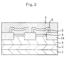
- Figure 2 is a cross-sectional view illustrating the structure of a memory transistor section taken in the direction X (i.e., a cross section including a gate width direction, see Figure 4(a) ) in the nonvolatile semiconductor memory device of the first embodiment.
- the floating gate electrodes 5 of adjacent memory transistors are electrically isolated from each other by an element isolating film 14 provided therebetween.
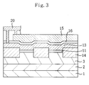
- Figure 3 is a cross-sectional view illustrating the structure of a select transistor section taken in the direction X in the nonvolatile semiconductor memory device of the first embodiment.
- the select gate electrode 13 is continuous among the select transistors adjacent to each other in the direction X , and is electrically short-circuited with the dummy electrode 15 at regular intervals through a metal interconnect 20 or the like on the element isolation film 14 .
- the select gate electrode 13 is not necessarily electrically short-circuited with the dummy electrode 15 .
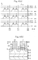
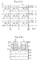
- Figure 4(a) is an electric circuit diagram illustrating voltages applied for simultaneously erasing data from all the memory cells in the nonvolatile semiconductor memory device of the first embodiment, while Figure 4(b) is a cross-sectional view illustrating how electrons move during the erase operation.
- the power supply voltage is assumed to be 1.5 V.
- each memory word line M.W-0 , 1 , 2 interconnects the control gate electrodes 7 of memory transistors arranged on the same row in the direction X .
- Each select word line S.W-0 , 1 , 2 interconnects the select gate electrodes 13 of select transistors arranged on the same row in the direction X .
- Each source line S-0 , 1 , 2 interconnects the source diffusion layers 9 of memory cells arranged on the same row in the direction X .
- each bit line B-0 , 1 , 2 interconnects the drain diffusion layers 8 of memory cells arranged on the same column in the direction Y .
- the source lines are disposed in parallel to the word lines for the memory cells (i.e., the memory word lines and the select word lines), while the bit lines are disposed vertically to the word lines.
- Figure 4(a) illustrates voltages applied for simultaneously erasing data from all of the nine memory cells illustrated.
- a voltage of -8 V is applied to the memory word lines M.W-0 , 1 , 2
- a voltage of +5 V is applied to the P-type well PW
- a voltage of 1.5 V is applied to the select word lines S.W-0 , 1 , 2 .
- the potential difference between the control gate electrode 7 and the surface of the channel is 13 V at every memory transistor.
- tunneling current flows from the floating gate electrode 5 into the entire surface region of the channel of the memory transistor, whereby electrons are ejected out of the floating gate electrode 5 .
- the threshold voltage of the memory transistor is about -1.5 V.
- the threshold voltage of the select transistor is set at about 0.6 V.
- the potential in the select word lines S.W-0 , 1 , 2 is set equal to the power supply voltage of 1.5 V, in order to weaken the electric field applied to the gate insulating film 11 (thickness: about 8 nm) of the select transistor.
- the electric field applied to the gate insulating film 11 of the select transistor is 4.4 MV/cm, which is less than 5 MV/cm as a general reference level below which reliability is ensured. Accordingly, the deterioration in reliability, resulting from the deterioration of the gate insulating film 11 , can be prevented.
- a potential equal to that applied to the P-type well 3 may be applied to the source lines S-0 , 1 , 2 and the bit lines B-0 , 1 , 2 .
- a voltage of 0 V (ground potential) may be applied to the memory word lines M.W-0 , 1 , 2 and a voltage of +13 V may be applied to the P-type well ( PW ) 3 .
- the peripheral circuits can be advantageously simplified.
- the absolute value of the positive voltage is larger (i.e., increases from 5 to 13), the breakdown voltage of the transistor should be increased.
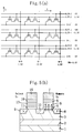
- Figure 5(a) is an electric circuit diagram illustrating voltages applied for writing data into only one memory cell located at the center and selected from the nine memory cells in the nonvolatile semiconductor memory device of this embodiment.
- Figure 5(b) is a cross-sectional view illustrating how electrons move during the write operation.
- a voltage of +9 V is applied to the memory word line M.W-1 connected to the control gate electrode of a selected memory cell.
- a voltage of -3.5 V is applied to the select word line S.W-1 connected to the select gate electrode of the selected memory cell.
- a voltage of -3.5 V is applied to the bit line B-1 connected to the drain diffusion layer of the selected memory cell.
- a voltage of 0 V is applied to the other memory word lines M.W-0 , 2
- a voltage of -3.5 V is applied to the other select word lines S.W-0 , 2
- a voltage of 1.5 V is applied to the other bit lines B-0 , 2 .
- a write operation may be performed by respectively applying voltages of +12.5 in, 0 V, 0 V and 0 V to the memory word line M.W-1 , the select word line S.W-1 and the bit line B-1 and the P-type well PW without applying any negative voltage.
- voltages of 0 V, 0 V and 5.0 V may be applied to the other memory word lines M.W-0 , 2 , the other select word lines S.W-0 , 2 and the other bit lines B-0 , 2 , respectively.
- the gate length of the select gate electrode 13 of the select transistor is set at about 0.5 ⁇ m in order to secure a source-to-drain breakdown voltage of about 5 V. Since the select gate electrode 13 of this embodiment is not in the shape of a sidewall unlike the memory cell of the conventional nonvolatile semiconductor memory device shown in Figure 28 , the gate length thereof may be set at an arbitrary value. The gap between the select transistor and the memory transistor is almost as large as a minimum design rule (e.g., about 0.3 ⁇ m). Accordingly, unlike the conventional nonvolatile semiconductor memory device shown in Figure 28 , the deterioration in reliability of the lateral interelectrode insulating film 112 has nothing to do with this embodiment.
- Figure 6(a) is an electric circuit diagram illustrating voltages applied for reading data from only one memory cell located at the center and selected from the nine memory cells in the nonvolatile semiconductor memory device of this embodiment.
- Figure 6(b) is a cross-sectional view illustrating how electrons move during the read operation.
- a voltage of 0 V is applied to all the memory word lines M.W-0 , 1 , 2 for all the memory cells.
- a voltage of 1.5 V is applied to the select word line S.W-1 connected to the selected memory cell, while a voltage of 0 V is applied to the other select word lines S.W-0 , 2 .
- a voltage of 1 V is applied to the bit line B-1 connected to the selected memory cell, while the other bit lines B-0 , 2 are opened. And a voltage of 0 V is applied to the P-type well PW .
- the current does not flow.
- the reading method of this embodiment there is no need to select a particular memory word line because the voltage applied to the select word line connected to the select gate electrode 13 of the selected memory cell is controlled during reading.
- the configuration of a decoder for a memory word line is complicated because the decoder is driven with a high positive or negative voltage.
- the configuration of a decoder for a select word line is simpler. Accordingly, such a reading method is advantageous in increasing a read speed, which should be far higher than a write speed or an erase speed.
- this method can also effectively suppress a gate read disturb phenomenon during reading.
- the "gate read disturb" is a phenomenon that data is erroneously written into or erased from a memory cell owing to a readout gate voltage applied to the control gate electrode.
- a positive voltage equal to or lower than the threshold voltage of a memory cell may be applied to the word lines for all the memory cells, or to only the memory word line of a selected memory cell.
- the method of this embodiment is the simplest of all of these.
- the nonvolatile semiconductor memory device of this embodiment can also attain all the advantages of the conventional nonvolatile semiconductor memory device shown in Figure 28 over the drain-side FN-FN type flash EEPROM. Specifically, the device of this embodiment
- the device of this embodiment can solve the following two disadvantages of the nonvolatile semiconductor memory device shown in Figure 28 :
- the nonvolatile semiconductor memory device of this embodiment can provide a highly implementable structure while simultaneously exhibiting satisfactory characteristics.
- the gate length of the select gate electrode of the select transistor should be 0.2 ⁇ m or more in the nonvolatile semiconductor memory device of the first embodiment.
- this device is somewhat disadvantage in terms of miniaturization.
- the present invention is applied to a fabrication process carried out under a design rule of about 0.35 ⁇ m, this increase in area of the gate electrode is negligible.
- a conventional flash EEPROM a single-transistor structure including only a memory transistor has prevailed in order to reduce the area occupied by the flash EEPROM.
- the nonvolatile semiconductor memory device of the present invention is particularly suitable for these applications.
- the source lines are provided independently in parallel to respective bit lines (vertically to respective word lines).
- the structures of the memory transistor and the select transistor are totally the same as those of the first embodiment, and the illustration and description thereof will be omitted herein.
- Figure 7 is an electric circuit diagram illustrating voltages applied during erasing in the nonvolatile semiconductor memory device of this embodiment.
- the power supply voltage is assumed to be 1.5 V.
- each memory word line M.W-0 , 1 , 2 interconnects the control gate electrodes 7 of memory transistors arranged on the same row in the direction X .
- Each select word line S.W-0 , 1 , 2 interconnects the select gate electrodes 13 of select transistors arranged on the same row in the direction X .
- Each source line S-0 , 1 , 2 interconnects the source diffusion layers 9 of memory cells arranged on the same column in the direction Y .
- each bit line B-0 , 1 , 2 interconnects the drain diffusion layers 8 of memory cells arranged on the same column in the direction Y .
- the array structure of this embodiment is different from that of the first embodiment in that not only the bit lines B-0 , 1 , 2 , but also the source lines S-0 , 1 , 2 are disposed vertically to the word lines for memory cells (i.e., the memory word lines M.W-0 , 1 , 2 and the select word lines S.W-0 , 1 , 2 ).
- each source line S-0 , 1 , 2 is provided electrically independently between a pair of memory cells adjacent to each other in the direction X .
- Figure 7 illustrates voltages applied for simultaneously erasing data from all of the nine memory cells illustrated.
- a voltage of -8 V is applied to all the memory word lines M.W-0 , 1 , 2 .
- a voltage of 1.5 V is applied to all the select word lines S.W-0 , 1 , 2 .
- All the bit lines B-0 , 1 , 2 and the source lines S-0 , 1 , 2 are opened.
- a voltage of +5 V is applied to the P-type well PW .
- the erase operation is performed in the same manner as in the first embodiment (see Figure 4(b) ), and the detailed description thereof will be omitted herein.
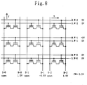
- Figure 8 is an electric circuit diagram illustrating voltages applied for writing data into only one memory cell located at the center and selected from the nine memory cells.
- a voltage of +9 V is applied to the memory word line M.W-1 connected to the control gate electrode of a selected memory cell.
- a voltage of 0 V is applied to the select word line S.W-1 connected to the select gate electrode of the selected memory cell.
- a voltage of -3.5 V is applied to the bit line B-1 connected to the drain diffusion layer of the selected memory cell.
- a voltage of -3.5 V is applied to the P-type well PW .
- the potential difference between the control gate electrode 7 of the memory transistor and the surface of the channel is 12.5 V at the selected memory cell.
- tunneling current flows from the entire surface region of the channel of the memory transistor into the floating gate electrode 5 of the memory transistor, whereby electrons are injected into the floating gate electrode 5 .
- the threshold voltage of the memory transistor is about 1 V.
- a voltage of 0 V is applied to the other memory word lines M.W-0 , 2 , and a voltage of 1.5 V is applied to the other bit lines B-0 , 2 .
- the potential difference between the control gate electrode 7 and the surface of the channel can be no greater than 7.5 V at the non-selected memory cells, and it is possible to prevent the data from being erroneously written into the non-selected memory cells.
- the select transistors need not be turned OFF unlike the first embodiment. This is because no leakage current is generated between bit lines through a source line, since the source lines are provided electrically independently in parallel to the respective bit lines.
- the applied voltage may be set at any other value.
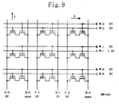
- Figure 9 is an electric circuit diagram illustrating voltages applied for reading data from only one memory cell located at the center and selected from the nine memory cells.
- a voltage of 0 V is applied to all the memory word lines M.W-0 , 1 , 2 for all the memory cells.
- a voltage of 1.5 V is applied to the select word line S.W-1 connected to the select gate electrode of a selected memory cell, while a voltage of 0 V is applied to the other select word lines S.W-0 , 2 .
- a voltage of 1 V is applied to the bit line B-1 connected to the drain diffusion layer of the selected memory cell, while the other bit lines B-0 , 2 are opened.
- a voltage of 0 V is applied to the P-type well PW .
- the read operation is performed in the same manner as in the first embodiment (see Figure 6(b) ), and the detailed description thereof will be omitted herein.
- a decoder for controlling a select word line may be a very small transistor having a breakdown voltage substantially as low as the power supply voltage (1.5 V).
- this embodiment is advantageous in reducing the area of a decoder for controlling the select word line and in realizing a higher-speed operation.
- the nonvolatile semiconductor memory device of this embodiment can also attain all of the advantages of the conventional nonvolatile semiconductor memory device shown in Figure 28 over the drain-side FN-FN type flash EEPROM. Specifically, the device of this embodiment
- the device of this embodiment can solve the following two disadvantages of the nonvolatile semiconductor memory device shown in Figure 28 :
- the gate length of the select gate electrode of the select transistor should be 0.2 ⁇ m or more in the first embodiment.
- the device of the first embodiment is somewhat disadvantage in terms of miniaturization.
- this second embodiment since the source lines are arranged in a different manner to solve this problem, there is no need to set the breakdown voltage of the select transistor at 5 V or more. Accordingly, it is no longer necessary to limit the gate length of a select gate electrode of the select transistor in order to solve the problem (2) barring the implementation of the nonvolatile semiconductor memory device shown in Figure 28 . Consequently, this embodiment is more advantageous than the first embodiment in terms of miniaturization.
- the third embodiment provides a means for eliminating such a disadvantage.
- source lines are also disposed electrically independently in parallel to respective bit lines (i.e., vertically to the word lines).
- the structures of the memory transistor and the select transistor are substantially the same as those of the first embodiment, and the illustration and description thereof will be omitted herein.
- these transistors are disposed in an opposite manner to the first and second embodiments. That is to say, in a memory cell of this embodiment, a memory transistor is disposed adjacent to the source diffusion layer 9 and a select transistor is disposed adjacent to the drain diffusion layer 8 .
- Figure 10(a) is an electric circuit diagram illustrating voltages applied for simultaneously erasing data from all the memory cells in the nonvolatile semiconductor memory device of the third embodiment, while Figure 10(b) is a cross-sectional view illustrating how electrons move during the erase operation.
- the power supply voltage is assumed to be 1.5 V.
- the array structure of this embodiment is the same as the array structure of the second embodiment shown in Figure 7 .
- the nonvolatile semiconductor memory device of the third embodiment also performs the erase method and operation in the same way as the device of the second embodiment (see Figures 7 and 10(a) ). Specifically, by applying the voltages shown in Figure 10(a) , tunneling current flows from the floating gate electrode 5 into the entire surface region of the channel of the memory transistor, whereby electrons are ejected out of the floating gate electrode 5 as shown in Figure 10(b) .
- Figure 11(a) is an electric circuit diagram illustrating voltages applied for writing data into only one memory cell located at the center and selected from the memory cells in the nonvolatile semiconductor memory device of the third embodiment.
- Figure 11(b) is a cross-sectional view illustrating how electrons move during the write operation.
- a voltage of +9 V is applied to the memory word line M.W-1 connected to the control gate electrode of a selected memory cell.
- a voltage of 0 V is applied to the select word line S.W-1 connected to the select gate electrode of the selected memory cell.
- a voltage of -3.5 V is applied to the source line S-1 connected to the source diffusion layer of the selected memory cell.
- a voltage of 0 V is applied to the other memory word lines M.W-0 , 2 and select word lines S.W-0 , 2 and a voltage of 1.5 V is applied to the other source lines S-0 , 2 .
- the potential difference between the control gate electrode 7 and the surface of the channel can be no greater than 7.5 V at the memory transistors of the non-selected memory cells. Consequently, it is possible to prevent the data from being erroneously written into the non-selected memory cells.
- the bit lines B-0 , 1 , 2 are all opened in this embodiment.
- the memory transistor since the memory transistor is disposed adjacent to the source diffusion layer 9 , it is no longer necessary to apply a negative voltage to the bit line connected to the selected memory cell during writing.
- Figure 12(a) is an electric circuit diagram illustrating voltages applied for reading data from only one memory cell located at the center and selected from the memory cells in the nonvolatile semiconductor memory device of the third embodiment.
- Figure 12(b) is a cross-sectional view illustrating how electrons move during the read operation.
- the voltages applied for reading as shown in Figure 12(a) are the same as those applied for reading in the second embodiment (see Figure 9 ).
- As a result of the application of these voltages in a memory cell in erase state, electrons move and current flows as shown in Figure 12(b) . On the other hand, in the other memory cells in write state, the current does not flow.
- drain disturb is a phenomenon that data is erroneously written into or erased from a memory cell because of a readout drain voltage applied to a drain.
- the nonvolatile semiconductor memory device of this embodiment can also attain all of the advantages of the conventional nonvolatile semiconductor memory device shown in Figure 28 over the drain-side FN-FN type flash EEPROM. Specifically, the device of this embodiment
- the device of this embodiment can solve the following two disadvantages of the nonvolatile semiconductor memory device shown in Figure 28 :
- the nonvolatile semiconductor memory device of this embodiment can provide a highly implementable structure while simultaneously exhibiting satisfactory characteristics.
- this embodiment is advantageous over the first and second embodiments on the following points.
- positive and negative voltages should be both applied to the bit lines, and therefore, the configuration of a bit line driver is adversely complicated.
- a bit line driver includes a read circuit, an overly complicated bit line driver is disadvantageous to the implementation of a high-speed read operation.
- the memory transistor is disposed adjacent to the source diffusion layer 9 of a memory cell, and it is no longer necessary to apply a negative voltage to the bit lines.
- the configuration of a bit line driver can be simplified and this embodiment is advantageous to the implementation of a high-speed read operation.
- a voltage of -3.5 V is applied to the P-type well and a voltage of 1.5 V is applied to a bit line or a source line during a write operation.
- a sufficient breakdown voltage should be secured between the diffusion layer and the P-type well.
- Such a high breakdown voltage possibly bars further miniaturisation.
- source lines are disposed electrically independently in parallel to respective bit lines (i.e., vertically to the word lines).
- the P-type well 3 are also divided into a plurality of electrically independent regions parallel to respective bit lines.
- Figure 13 is a cross-sectional view illustrating the structure of a memory transistor section taken in the direction X in the nonvolatile semiconductor memory device of the fourth embodiment. It is noted that the cross section of the memory transistor section taken in the direction Y in the nonvolatile semiconductor memory device of the fourth embodiment is the same as that of the nonvolatile semiconductor memory device of the third embodiment shown in Figure 10(b) . That is to say, the memory transistor is disposed adjacent to the source diffusion layer 9 and the select transistor is disposed adjacent to the drain diffusion layer 8 .
- a well-isolating film 18 is provided to divide the P-type well 3 into three electrically isolated regions 3a , 3b and 3c in the direction X .
- the floating gate electrodes 5 of the respective memory transistors are electrically isolated from each other by the well-isolating film 18 .
- the well-isolating film 18 extends straight in the direction Y .
- a plurality of memory cells located on the same cross section taken in the direction Y , are disposed within the same P-type well 3a , 3b or 3c .
- the bottom of the P-type well 3 is electrically isolated from the P-type semiconductor substrate 1 by the deep N-type well 2 .
- an SOI (silicon on insulator) structure may be employed, i.e., the well 3 and the substrate 1 may be isolated from each other by an insulating film.
- Figure 14 is a cross-sectional view illustrating the structure of a select transistor section taken in the direction X in the nonvolatile semiconductor memory device of the fourth embodiment.
- the select gate electrode 13 is continuous among the select transistors adjacent to each other in the direction X , and is electrically short-circuited at regular intervals with the dummy electrode 15 through a metal interconnect 20 or the like on the well-isolating film 18 .
- the select gate electrode 13 is not necessarily electrically short-circuited with the dummy electrode 15 .
- Figure 15 is an electric circuit diagram illustrating voltages applied during an erase operation of the nonvolatile semiconductor memory device of the fourth embodiment.
- the power supply voltage is assumed to be 1.5 V.
- the array structure of the non-volatile semiconductor memory device of the fourth embodiment is the same as that of the third embodiment.
- a plurality of memory cells arranged in the direction Y are disposed in common within the same one of P-type well regions 3a , 3b or 3c , isolated from each other and provided for the respective memory cells adjacent to each other in the direction X .
- well contact lines PW-0 , 1 , 2 are provided to make contact with the respective P-type well regions 3a , 3b and 3c .
- different voltages may be applied independently by respective decoders to the P-type well regions 3a , 3b and 3c.
- a voltage of 5 V is applied to the well contact lines PW-0 , 1 , 2 , connected to the P-type well regions 3a , 3b and 3c , respectively, during an erase operation. Accordingly, the same voltages as those applied in the third embodiment (see Figure 10(a) ) are applied during this erase operation after all. Thus, the description thereof will be omitted herein.
- Figure 16 is an electric circuit diagram illustrating voltages applied for writing data into only one memory cell located at the center and selected from the memory cells in the nonvolatile semiconductor memory device of the fourth embodiment.
- a voltage of +9 V is applied to the memory word line M.W-1 connected to the control gate electrode of the selected memory cell.
- a voltage of 0 V is applied to the select word line S.W-1 connected to the select gate electrode of the selected memory cell.
- a voltage of -3.5 V is applied to the source line S-1 connected to the source diffusion layer of the selected memory cell.
- a voltage of 0 V is applied to the other memory word lines M.W-0 , 2 and select word lines S.W-0 , 2 , and a voltage of 1.5 V is applied to the other source lines S-0 , 2 and well contact lines PW-0 , 2 .
- the potential difference between the control gate electrode 7 and the surface of the channel can be no greater than 7.5 V at the memory transistors of the non-selected memory cells. Consequently, it is possible to prevent the data from being erroneously written into the non-selected memory cells.
- the bit lines B-0 , 1 , 2 are all opened in this embodiment, thereby simplifying the control operation as much as possible.
- the nonvolatile semiconductor memory device of this embodiment can control in this manner the potential in the P-type well for non-selected memory cells on a bit line basis. Accordingly, since the potential difference between the source diffusion layer 9 (or the drain diffusion layer 8 ) and the P-type well 3 can be 0 V, it is no longer necessary to secure a high breakdown voltage for this part.
- Figure 17 is an electric circuit diagram illustrating voltages applied for reading data from only one memory cell located at the center and selected from the memory cells in the nonvolatile semiconductor memory device of the fourth embodiment.
- the voltages applied for reading as shown in Figure 17 are the same as those applied for reading in the third embodiment (see Figure 12(a) ), because a voltage of 0 V is applied to the respective well contact lines PW-0 , 1 , 2 .
- a voltage of 0 V is applied to the respective well contact lines PW-0 , 1 , 2 .
- the nonvolatile semiconductor memory device of this embodiment can also attain all of the advantages of the conventional nonvolatile semiconductor memory device shown in Figure 28 over the drain-side FN-FN type flash EEPROM. Specifically, the device of this embodiment
- the device of this embodiment can solve the following two disadvantages of the nonvolatile semiconductor memory device shown in Figure 28 :
- the nonvolatile semiconductor memory device of this embodiment can provide a highly implementable structure while simultaneously exhibiting satisfactory characteristics.
- this embodiment is advantageous over the first, second and third embodiments on the following points.
- a potential difference of about 5 V is generated between the source diffusion layer 9 (or the drain diffusion layer 8 ) and the P-type well 3 .
- a high breakdown voltage should be secured between the diffusion layer and the well. Accordingly, if the design rule should be defined at as small as about 0.2 ⁇ m or less, problems happen.
- source lines are disposed electrically independently in parallel to respective bit lines (i.e., vertically to the word lines) and the P-type well 3 are also divided into a plurality of electrically isolated regions parallel to respective bit lines.
- this embodiment it is easy to set the potential difference between the source diffusion layer 9 (or the drain diffusion layer 8 ) and the P-type well at 0 V. Therefore, this embodiment is advantageous to miniaturization requiring a design rule of 0.2 ⁇ m or less.
- a memory transistor is disposed adjacent to the source diffusion layer 9 , while a select transistor is disposed adjacent to the drain diffusion layer 8 .
- these transistors may be disposed in an opposite fashion.
- the present invention is not limited to such an embodiment.
- Figure 18 is an electric circuit diagram illustrating voltages applied for performing an erase operation by injecting electrons into the floating gate electrode 5 .
- Figure 19 is an electric circuit diagram illustrating voltages applied for performing a write operation by ejecting electrons out of the floating gate electrode 5 .
- the threshold voltages defined for writing and erasing may be inverted. The effects attained by this inversion will be described in the next embodiment.
- a memory transistor and a select transistor are both required. Specifically, in the first embodiment, a select transistor should be provided adjacent to the source region of a memory cell so that the source lines disposed along the word lines may be opened. In the second, third and fourth embodiments, the operation of simultaneously erasing data from a plurality of memory cells is performed by ejecting electrons out of the floating gate electrode 5 (the threshold voltage decreases). Thus, a select transistor should also be provided (either in the source region or in the drain region) to avoid the problem of excessive erasure.
- the nonvolatile semiconductor memory device of the foregoing embodiments is disadvantageous over the conventional drain-side FN-FN type flash EEPROM shown in Figure 24 in that the area occupied by a memory cell increases in these embodiments.
- a nonvolatile semiconductor memory device which can avoid the increase in area of a memory cell, will be described as the fifth embodiment.
- source lines are also disposed electrically independently in parallel to respective bit lines (i.e., vertically to the word lines).
- the P-type well 3 are also divided into a plurality of electrically isolated regions parallel to the respective bit lines.
- a memory cell of this embodiment includes only a memory transistor, not a select transistor.
- Figure 20 is a cross-sectional view illustrating the structure of a memory transistor section taken in the direction Y in the nonvolatile semiconductor memory device of the fifth embodiment.
- the memory cell of this embodiment includes only the same components (identified by the same reference numerals) as the nonvolatile semiconductor memory device of the first embodiment shown in Figure 1 , and the description thereof will be omitted herein.
- the memory cell of this embodiment includes only the memory transistor and is not provided with any select transistor.
- Figure 21 is an electric circuit diagram illustrating voltages applied during an erase operation of the nonvolatile semiconductor memory device of the fifth embodiment.
- the power supply voltage is assumed to be 1.5 V.
- each memory word line M.W-0 , 1 , 2 interconnects the control gate electrodes 7 of memory transistors arranged on the same row in the direction X .
- Each source line S-0 , 1 , 2 interconnects the source diffusion layers 9 of memory cells arranged on the same column in the direction Y .
- each bit line B-0 , 1 , 2 interconnects the drain diffusion layers 8 of memory cells arranged on the same column in the direction Y .
- the source lines S-0 , 1 , 2 and the bit lines B-0 , 1 , 2 are disposed vertically to the word lines for memory cells (i.e., the memory word lines M.W-0 , 1 , 2 ).
- the source lines S-0 , 1 , 2 are provided for the respective bit lines B-0 , 1 , 2 and are electrically isolated from each other between memory cells adjacent to each other in the direction X .
- the P-type well 3 is divided into respective electrically isolated regions between memory cells adjacent to each other in the direction X . And the potentials in the P-type well regions 3 are controllable by using decoders for well contact lines PW-0 , 1 , 2 .
- Figure 21 illustrates the voltages applied for simultaneously erasing data from all of the nine memory cells illustrated.
- a voltage of +9 V is applied to all the memory word lines M.W-0 , 1 , 2 and a voltage of -3.5 V is applied to all the well contact lines PW-0 , 1 , 2 .
- the potential difference between the control gate electrode 7 and the surface of the channel is 12.5 V at every memory transistor. Consequently, tunneling current flows from the entire surface region of the channel into the floating gate electrode 5 at the memory transistor, whereby electrons are injected into the floating gate electrode 5 .
- the threshold voltage of the memory transistor is about 2.0 V.
- Figure 22 is an electric circuit diagram illustrating voltages applied for writing data into only one memory cell located at the center and selected from the nine memory cells in the non-volatile semiconductor memory device of this embodiment.
- a voltage of -8 V is applied to the memory word line M.W-1 connected to the control gate electrode of a selected memory cell.
- a voltage of 5 V is applied to the well contact line PW-1 connected to the P-type well of the selected memory cell.
- the potential difference between the control gate electrode 7 and the surface of the channel is 13 V at the memory transistor of the selected memory cell. Consequently, tunneling current flows from the floating gate electrode 5 into the entire surface of the channel, whereby electrons are ejected out of the floating gate electrode 5 .
- the threshold voltage of the memory transistor is about 0.5 V.
- a voltage of 0 V is applied to the other memory word lines M.W-0 , 2 and well contact lines PW-0 , 2 .
- the potential difference between the control gate electrode 7 and the surface of the channel can be no greater than 8 V at the memory transistors of the non-selected memory cells. Consequently, it is possible to prevent the data from being erroneously written into non-selected memory cells.
- all the bit lines B-0 , 1 , 2 and source lines S-0 , 1 , 2 may be either opened (about 0 V) or set at respective potentials equal to those of the P-type well regions connected to the bit lines and source lines.
- the threshold voltage can be in a controllable write state on a bit-by-bit basis during a write operation performed by ejecting electrons (threshold voltage decreases). Accordingly, a memory cell can include only a memory transistor while avoiding the problem of excessive erasure.
- Figure 23 is an electric circuit diagram illustrating voltages applied for reading data from only one memory cell located at the center and selected from the nine memory cells in the nonvolatile semiconductor memory device of this embodiment.
- a voltage of 1.5 V is applied to the memory word line M.W-1 connected to the control gate electrode of the selected memory cell, while a voltage of 0 V is applied to the other memory word lines M-0 , 2 .
- a voltage of 1 V is applied to the bit line B-1 connected to the drain diffusion layer of the selected memory cell, while the other bit lines B-0 , 2 are opened.
- the nonvolatile semiconductor memory device of this embodiment can also attain all of the advantages of the conventional nonvolatile semiconductor memory device shown in Figure 28 over the drain-side FN-FN type flash EEPROM. Specifically, the device of this embodiment
- the device of this embodiment can solve the following two disadvantages of the nonvolatile semiconductor memory device shown in Figure 28 :
- the nonvolatile semiconductor memory device of this embodiment can provide a highly implementable structure while simultaneously exhibiting satisfactory characteristics.
- the nonvolatile semiconductor memory device of this embodiment does not include any select transistor but includes only a memory transistor, the area occupied by a single memory cell can be reduced as compared with the nonvolatile semiconductor memory device shown in Figure 28 .
- circuit designing technologies are required for controlling the write depth (threshold voltage) of a memory cell bit by bit to be distributed within a narrow range (e.g., from 0.6 V to 0.8 V).
- Figures 33 through 35 are electric circuit diagrams illustrating voltages applied for performing erase, write and read operations, respectively, in a conventional nonvolatile semiconductor memory device disclosed in Japanese Laid-Open Publication No. 8-279566.
- the structure of a memory cell in the nonvolatile semiconductor memory device described in this publication is similar to that of the memory cell in the fifth embodiment shown in Figure 20 .
- the memory cell described in the publication is configured to apply an equal potential to all the wells provided for the respective columns, not to independently control the potentials in the respective well regions as in the fifth embodiment. This is because, in the memory cells of the publication, the wells are provided for the respective columns just to suppress leakage current between adjacent columns.
- the threshold voltages and the operations for writing and erasing are defined in mutually opposite manners.
- Figure 32(a) is a graph illustrating the distributions of threshold voltages of a memory cell after write and erase operations have been performed by the memory cell of this embodiment.
- Figure 32(b) is a graph illustrating the distributions of threshold voltages of a memory cell after write and erase operations have been performed by the memory cell of the above identified publication.
- the threshold voltage in erase state (where the threshold voltage is high) is in the range from 2.0 V to 3.0 V in this embodiment.
- the threshold voltage in the erase state in this embodiment is much lower than the threshold voltage of 3.0 V to 3.5 V in the write state (where the threshold voltage is high) in accordance with the technology disclosed in the publication.
- the lower threshold voltages are approximately equal to each other in both this embodiment and the prior art.
- the distribution of lower threshold voltages should be controlled to have a narrower range.
- the write or erase operation should be controlled on a bit-by-bit basis.
- the respective well regions are coded, it is possible to decrease only the threshold voltage of a particular memory cell located at the intersection between a well region and a word line, and therefore, the operation can be controlled on a bit-by-bit basis.
- control cannot be performed but to set the potentials in the respective wells at an equal value, and it is difficult to decrease only the threshold voltage of a particular bit.
- an operation at 1.5 V is enabled in accordance with this embodiment. That is a prominent effect attainable only by this embodiment.
- the technology disclosed in the above-identified publication can solve two out of the three conventional problems, i.e., (1) improvement of reliability and (2) reduction of power consumption during writing.
Landscapes
- Engineering & Computer Science (AREA)
- Microelectronics & Electronic Packaging (AREA)
- Non-Volatile Memory (AREA)
- Semiconductor Memories (AREA)
- Read Only Memory (AREA)
Applications Claiming Priority (2)
| Application Number | Priority Date | Filing Date | Title |
|---|---|---|---|
| JP33954897A JP3378879B2 (ja) | 1997-12-10 | 1997-12-10 | 不揮発性半導体記憶装置及びその駆動方法 |
| JP33954897 | 1997-12-10 |
Publications (2)
| Publication Number | Publication Date |
|---|---|
| EP0924768A2 true EP0924768A2 (de) | 1999-06-23 |
| EP0924768A3 EP0924768A3 (de) | 2000-03-01 |
Family
ID=18328519
Family Applications (1)
| Application Number | Title | Priority Date | Filing Date |
|---|---|---|---|
| EP98123178A Withdrawn EP0924768A3 (de) | 1997-12-10 | 1998-12-04 | Halbleiterspeicheranordnung und deren Betriebsverfahren |
Country Status (4)
| Country | Link |
|---|---|
| US (3) | US6169307B1 (de) |
| EP (1) | EP0924768A3 (de) |
| JP (1) | JP3378879B2 (de) |
| TW (1) | TW430997B (de) |
Cited By (4)
| Publication number | Priority date | Publication date | Assignee | Title |
|---|---|---|---|---|
| WO2002071408A1 (en) * | 2001-03-05 | 2002-09-12 | Microchip Technology Incorporated | Split common source on eeprom array |
| US6980461B2 (en) | 2003-05-13 | 2005-12-27 | Innovative Silicon S.A. | Reference current generator, and method of programming, adjusting and/or operating same |
| US7736959B2 (en) | 2003-07-22 | 2010-06-15 | Innovative Silicon Isi Sa | Integrated circuit device, and method of fabricating same |
| CN111739571A (zh) * | 2019-03-25 | 2020-10-02 | 亿而得微电子股份有限公司 | 低电流电子可擦除可重写只读存储器阵列的快速擦除方法 |
Families Citing this family (67)
| Publication number | Priority date | Publication date | Assignee | Title |
|---|---|---|---|---|
| JP3378879B2 (ja) | 1997-12-10 | 2003-02-17 | 松下電器産業株式会社 | 不揮発性半導体記憶装置及びその駆動方法 |
| JP2000068484A (ja) | 1998-08-19 | 2000-03-03 | Nec Corp | 不揮発性半導体記憶装置及びその製造方法並びに不揮発 性半導体記憶装置を内蔵したマイクロコンピュータ及び その製造方法 |
| US6501680B1 (en) * | 1999-10-07 | 2002-12-31 | Hyundai Electronics Industries Co., Ltd. | Nonvolatile memory, cell array thereof, and method for sensing data therefrom |
| US6577531B2 (en) * | 2000-04-27 | 2003-06-10 | Semiconductor Energy Laboratory Co., Ltd. | Nonvolatile memory and semiconductor device |
| KR100386611B1 (ko) * | 2000-05-08 | 2003-06-02 | 주식회사 하이닉스반도체 | 플래쉬 메모리 셀의 어레이와 그를 이용한 데이터프로그램방법과 소거방법 |
| JP4823408B2 (ja) | 2000-06-08 | 2011-11-24 | ルネサスエレクトロニクス株式会社 | 不揮発性半導体記憶装置 |
| US6438030B1 (en) * | 2000-08-15 | 2002-08-20 | Motorola, Inc. | Non-volatile memory, method of manufacture, and method of programming |
| US20020096707A1 (en) * | 2001-01-24 | 2002-07-25 | Rudeck Paul J. | Modified source/drain re-oxidation method and system |
| JP4574912B2 (ja) * | 2001-08-22 | 2010-11-04 | シャープ株式会社 | 半導体記憶装置の形成方法 |
| JP2003068894A (ja) * | 2001-08-29 | 2003-03-07 | Sharp Corp | 半導体記憶装置およびその形成方法 |
| JP2003203997A (ja) * | 2002-01-07 | 2003-07-18 | Mitsubishi Electric Corp | 不揮発性半導体記憶装置及びその製造方法 |
| JP3978062B2 (ja) | 2002-03-26 | 2007-09-19 | 松下電器産業株式会社 | 半導体記憶素子への電圧印加方法及び半導体記憶装置 |
| US6747896B2 (en) | 2002-05-06 | 2004-06-08 | Multi Level Memory Technology | Bi-directional floating gate nonvolatile memory |
| US7221591B1 (en) | 2002-05-06 | 2007-05-22 | Samsung Electronics Co., Ltd. | Fabricating bi-directional nonvolatile memory cells |
| US6914820B1 (en) | 2002-05-06 | 2005-07-05 | Multi Level Memory Technology | Erasing storage nodes in a bi-directional nonvolatile memory cell |
| KR100442883B1 (ko) * | 2002-09-11 | 2004-08-02 | 삼성전자주식회사 | 측벽 게이트와 sonos 셀 구조를 갖는 불휘발성메모리 소자의 제조 방법 |
| JP3914869B2 (ja) | 2002-12-20 | 2007-05-16 | スパンション インク | 不揮発性メモリ及びその書き換え方法 |
| US6819594B2 (en) * | 2003-01-06 | 2004-11-16 | Ememory Technology Inc. | Electrically erasable programmable logic device |
| US6962852B2 (en) | 2003-03-19 | 2005-11-08 | Promos Technologies Inc. | Nonvolatile memories and methods of fabrication |
| US6962851B2 (en) * | 2003-03-19 | 2005-11-08 | Promos Technologies, Inc. | Nonvolatile memories and methods of fabrication |
| US6995060B2 (en) * | 2003-03-19 | 2006-02-07 | Promos Technologies Inc. | Fabrication of integrated circuit elements in structures with protruding features |
| US6893921B2 (en) * | 2003-04-10 | 2005-05-17 | Mosel Vitelic, Inc. | Nonvolatile memories with a floating gate having an upward protrusion |
| JP3884397B2 (ja) | 2003-04-25 | 2007-02-21 | 株式会社東芝 | 不揮発性半導体記憶装置 |
| US6902974B2 (en) * | 2003-05-16 | 2005-06-07 | Promos Technologies Inc. | Fabrication of conductive gates for nonvolatile memories from layers with protruding portions |
| US6846712B2 (en) | 2003-05-16 | 2005-01-25 | Promos Technologies Inc. | Fabrication of gate dielectric in nonvolatile memories having select, floating and control gates |
| US7214585B2 (en) * | 2003-05-16 | 2007-05-08 | Promos Technologies Inc. | Methods of fabricating integrated circuits with openings that allow electrical contact to conductive features having self-aligned edges |
| US6974739B2 (en) * | 2003-05-16 | 2005-12-13 | Promos Technologies Inc. | Fabrication of dielectric on a gate surface to insulate the gate from another element of an integrated circuit |
| US6955967B2 (en) * | 2003-06-27 | 2005-10-18 | Freescale Semiconductor, Inc. | Non-volatile memory having a reference transistor and method for forming |
| US6885044B2 (en) | 2003-07-30 | 2005-04-26 | Promos Technologies, Inc. | Arrays of nonvolatile memory cells wherein each cell has two conductive floating gates |
| US6951782B2 (en) * | 2003-07-30 | 2005-10-04 | Promos Technologies, Inc. | Nonvolatile memory cell with multiple floating gates formed after the select gate and having upward protrusions |
| US7169667B2 (en) | 2003-07-30 | 2007-01-30 | Promos Technologies Inc. | Nonvolatile memory cell with multiple floating gates formed after the select gate |
| US7052947B2 (en) * | 2003-07-30 | 2006-05-30 | Promos Technologies Inc. | Fabrication of gate dielectric in nonvolatile memories in which a memory cell has multiple floating gates |
| US7101757B2 (en) * | 2003-07-30 | 2006-09-05 | Promos Technologies, Inc. | Nonvolatile memory cells with buried channel transistors |
| US7060565B2 (en) * | 2003-07-30 | 2006-06-13 | Promos Technologies Inc. | Fabrication of dielectric for a nonvolatile memory cell having multiple floating gates |
| JP2005085404A (ja) | 2003-09-10 | 2005-03-31 | Matsushita Electric Ind Co Ltd | 半導体記憶装置 |
| US7238575B2 (en) * | 2004-03-10 | 2007-07-03 | Promos Technologies, Inc. | Fabrication of conductive lines interconnecting conductive gates in nonvolatile memories, and non-volatile memory structures |
| US7148104B2 (en) * | 2004-03-10 | 2006-12-12 | Promos Technologies Inc. | Fabrication of conductive lines interconnecting first conductive gates in nonvolatile memories having second conductive gates provided by conductive gate lines, wherein the adjacent conductive gate lines for the adjacent columns are spaced from each other, and non-volatile memory structures |
| JP2005332502A (ja) * | 2004-05-20 | 2005-12-02 | Renesas Technology Corp | 半導体装置およびicカード |
| JP2006060030A (ja) * | 2004-08-20 | 2006-03-02 | Renesas Technology Corp | 半導体記憶装置 |
| JP4338656B2 (ja) | 2005-02-15 | 2009-10-07 | 富士通マイクロエレクトロニクス株式会社 | 半導体記憶装置の書き込み方法 |
| US20070099386A1 (en) * | 2005-10-31 | 2007-05-03 | International Business Machines Corporation | Integration scheme for high gain fet in standard cmos process |
| US20070120173A1 (en) * | 2005-11-28 | 2007-05-31 | Bohumil Lojek | Non-volatile memory cell with high current output line |
| JP2007208036A (ja) * | 2006-02-02 | 2007-08-16 | Sanken Electric Co Ltd | 半導体素子 |
| KR100843141B1 (ko) * | 2006-05-19 | 2008-07-02 | 삼성전자주식회사 | 비휘발성 메모리 집적 회로 장치 및 그 제조 방법 |
| TWI466269B (zh) * | 2006-07-14 | 2014-12-21 | Semiconductor Energy Lab | 非揮發性記憶體 |
| JP4856488B2 (ja) * | 2006-07-27 | 2012-01-18 | ルネサスエレクトロニクス株式会社 | 半導体装置 |
| KR100852236B1 (ko) | 2006-09-05 | 2008-08-13 | 삼성전자주식회사 | 이이피롬 장치 및 그 제조 방법 |
| KR100851546B1 (ko) * | 2006-09-22 | 2008-08-11 | 삼성전자주식회사 | 비휘발성 기억 장치 및 그 동작 방법 |
| WO2008041303A1 (en) | 2006-09-29 | 2008-04-10 | Fujitsu Limited | Nonvolatile semiconductor storage apparatus, reading method thereof, writing method thereof and erasing method thereof |
| CN101512664B (zh) | 2006-09-29 | 2012-10-24 | 富士通半导体股份有限公司 | 非易失性半导体存储器件及其读取、写入和删除方法 |
| US8325530B2 (en) * | 2006-10-03 | 2012-12-04 | Macronix International Co., Ltd. | Cell operation methods using gate-injection for floating gate NAND flash memory |
| KR100861749B1 (ko) | 2006-12-22 | 2008-10-09 | 최웅림 | 2t nor형 비휘발성 메모리 셀 어레이, 2t nor형비휘발성 메모리의 데이터 처리방법 |
| US8320191B2 (en) | 2007-08-30 | 2012-11-27 | Infineon Technologies Ag | Memory cell arrangement, method for controlling a memory cell, memory array and electronic device |
| JP2009130136A (ja) * | 2007-11-22 | 2009-06-11 | Renesas Technology Corp | 不揮発性半導体記憶装置およびその製造方法 |
| EP2264756B1 (de) | 2008-03-31 | 2012-08-29 | Fujitsu Semiconductor Limited | Halbleiterbauelement |
| JP5458526B2 (ja) | 2008-08-08 | 2014-04-02 | 富士通セミコンダクター株式会社 | 半導体装置及びその製造方法 |
| US8446779B2 (en) * | 2009-08-21 | 2013-05-21 | Globalfoundries Singapore Pte. Ltd. | Non-volatile memory using pyramidal nanocrystals as electron storage elements |
| JP2010239147A (ja) * | 2010-06-09 | 2010-10-21 | Renesas Electronics Corp | 不揮発性半導体記憶装置 |
| CN102779552B (zh) * | 2011-05-11 | 2015-09-09 | 旺宏电子股份有限公司 | 记忆体的程序化方法及记忆体阵列中记忆胞的程序化方法 |
| KR101832934B1 (ko) | 2012-01-27 | 2018-02-28 | 삼성전자주식회사 | 비휘발성 메모리 장치, 그것을 포함하는 메모리 시스템, 그것의 블록 관리 방법, 프로그램 방법 및 소거 방법 |
| US9355725B2 (en) * | 2013-12-12 | 2016-05-31 | Cypress Semiconductor Corporation | Non-volatile memory and method of operating the same |
| US9847109B2 (en) * | 2015-12-21 | 2017-12-19 | Imec Vzw | Memory cell |
| FR3071355B1 (fr) | 2017-09-20 | 2019-08-30 | Stmicroelectronics (Rousset) Sas | Cellule-memoire eeprom compacte |
| CN110546708B (zh) * | 2017-12-15 | 2023-04-21 | 成都锐成芯微科技股份有限公司 | 快闪存储器的编程电路、编程方法及快闪存储器 |
| KR102791813B1 (ko) * | 2019-05-16 | 2025-04-08 | 에스케이하이닉스 주식회사 | 메모리 장치, 메모리 장치를 포함하는 메모리 시스템 및 메모리 시스템의 동작 방법 |
| JP7462389B2 (ja) * | 2019-07-18 | 2024-04-05 | ローム株式会社 | 不揮発性半導体記憶装置 |
| CN111129017B (zh) * | 2019-12-26 | 2022-06-07 | 华虹半导体(无锡)有限公司 | Otp存储器及其制造方法 |
Citations (2)
| Publication number | Priority date | Publication date | Assignee | Title |
|---|---|---|---|---|
| US5559735A (en) | 1995-03-28 | 1996-09-24 | Oki Electric Industry Co., Ltd. | Flash memory having select transistors |
| EP0778623A2 (de) | 1995-11-14 | 1997-06-11 | Programmable Microelectronics Corporation | Durch heisse Elektroneninjektion programmierbare und durch Tunneleffekt löschbare PMOS-Speicherzelle |
Family Cites Families (26)
| Publication number | Priority date | Publication date | Assignee | Title |
|---|---|---|---|---|
| JPS61281546A (ja) | 1985-06-07 | 1986-12-11 | Hitachi Ltd | 半導体集積回路装置 |
| JPH0754632B2 (ja) | 1985-10-25 | 1995-06-07 | 日立超エル・エス・アイエンジニアリング | 半導体記憶装置 |
| JPS62113478A (ja) | 1985-11-13 | 1987-05-25 | Toshiba Corp | 不揮発性半導体メモリ |
| JPH04123471A (ja) * | 1990-09-14 | 1992-04-23 | Oki Electric Ind Co Ltd | 半導体記憶装置のデータ書込みおよび消去方法 |
| JP2655765B2 (ja) | 1991-05-29 | 1997-09-24 | ローム株式会社 | 半導体装置 |
| JPH0644791A (ja) * | 1992-05-08 | 1994-02-18 | Seiko Epson Corp | 不揮発性半導体装置 |
| JPH065870A (ja) | 1992-06-16 | 1994-01-14 | Fujitsu Ltd | 半導体記憶装置 |
| JPH06120515A (ja) | 1992-10-09 | 1994-04-28 | Oki Electric Ind Co Ltd | 半導体不揮発性メモリのデータ書き込み及びデータ消去方法 |
| JPH06334156A (ja) | 1993-05-21 | 1994-12-02 | Sony Corp | Nor型フラッシュメモリ |
| US5513319A (en) | 1993-07-02 | 1996-04-30 | Dell Usa, L.P. | Watchdog timer for computer system reset |
| US5515319A (en) * | 1993-10-12 | 1996-05-07 | Texas Instruments Incorporated | Non-volatile memory cell and level shifter |
| JPH0817949A (ja) * | 1994-03-25 | 1996-01-19 | Nippon Steel Corp | 不揮発性半導体記憶装置及びその製造方法 |
| US5793081A (en) * | 1994-03-25 | 1998-08-11 | Nippon Steel Corporation | Nonvolatile semiconductor storage device and method of manufacturing |
| US5457652A (en) * | 1994-04-01 | 1995-10-10 | National Semiconductor Corporation | Low voltage EEPROM |
| US5471422A (en) * | 1994-04-11 | 1995-11-28 | Motorola, Inc. | EEPROM cell with isolation transistor and methods for making and operating the same |
| US5487033A (en) * | 1994-06-28 | 1996-01-23 | Intel Corporation | Structure and method for low current programming of flash EEPROMS |
| JPH08125041A (ja) | 1994-10-21 | 1996-05-17 | Sony Corp | 不揮発性半導体メモリ装置およびその読み出し/書き込み方法 |
| JP3328463B2 (ja) | 1995-04-06 | 2002-09-24 | 株式会社日立製作所 | 並列型不揮発性半導体記憶装置及び同装置の使用方法 |
| KR100413652B1 (ko) | 1995-09-11 | 2004-05-27 | 마츠시타 덴끼 산교 가부시키가이샤 | 반도체기억장치및그구동방법 |
| JP3323079B2 (ja) | 1995-09-11 | 2002-09-09 | 松下電器産業株式会社 | 半導体記憶装置,その駆動方法及びその製造方法 |
| AU7475196A (en) * | 1995-10-25 | 1997-05-15 | Nvx Corporation | Semiconductor non-volatile memory device having a nand cell structure |
| US5912842A (en) * | 1995-11-14 | 1999-06-15 | Programmable Microelectronics Corp. | Nonvolatile PMOS two transistor memory cell and array |
| JPH09199618A (ja) | 1996-01-23 | 1997-07-31 | Sony Corp | 不揮発性半導体記憶装置 |
| US5896315A (en) * | 1997-04-11 | 1999-04-20 | Programmable Silicon Solutions | Nonvolatile memory |
| US5867425A (en) * | 1997-04-11 | 1999-02-02 | Wong; Ting-Wah | Nonvolatile memory capable of using substrate hot electron injection |
| JP3378879B2 (ja) | 1997-12-10 | 2003-02-17 | 松下電器産業株式会社 | 不揮発性半導体記憶装置及びその駆動方法 |
-
1997
- 1997-12-10 JP JP33954897A patent/JP3378879B2/ja not_active Expired - Lifetime
-
1998
- 1998-12-03 TW TW087120087A patent/TW430997B/zh not_active IP Right Cessation
- 1998-12-04 EP EP98123178A patent/EP0924768A3/de not_active Withdrawn
- 1998-12-08 US US09/206,560 patent/US6169307B1/en not_active Expired - Lifetime
-
2000
- 2000-10-03 US US09/677,844 patent/US6377490B1/en not_active Expired - Fee Related
-
2002
- 2002-01-22 US US10/050,965 patent/US6657893B2/en not_active Expired - Lifetime
Patent Citations (2)
| Publication number | Priority date | Publication date | Assignee | Title |
|---|---|---|---|---|
| US5559735A (en) | 1995-03-28 | 1996-09-24 | Oki Electric Industry Co., Ltd. | Flash memory having select transistors |
| EP0778623A2 (de) | 1995-11-14 | 1997-06-11 | Programmable Microelectronics Corporation | Durch heisse Elektroneninjektion programmierbare und durch Tunneleffekt löschbare PMOS-Speicherzelle |
Cited By (4)
| Publication number | Priority date | Publication date | Assignee | Title |
|---|---|---|---|---|
| WO2002071408A1 (en) * | 2001-03-05 | 2002-09-12 | Microchip Technology Incorporated | Split common source on eeprom array |
| US6980461B2 (en) | 2003-05-13 | 2005-12-27 | Innovative Silicon S.A. | Reference current generator, and method of programming, adjusting and/or operating same |
| US7736959B2 (en) | 2003-07-22 | 2010-06-15 | Innovative Silicon Isi Sa | Integrated circuit device, and method of fabricating same |
| CN111739571A (zh) * | 2019-03-25 | 2020-10-02 | 亿而得微电子股份有限公司 | 低电流电子可擦除可重写只读存储器阵列的快速擦除方法 |
Also Published As
| Publication number | Publication date |
|---|---|
| JPH11177068A (ja) | 1999-07-02 |
| US6377490B1 (en) | 2002-04-23 |
| TW430997B (en) | 2001-04-21 |
| JP3378879B2 (ja) | 2003-02-17 |
| EP0924768A3 (de) | 2000-03-01 |
| US6169307B1 (en) | 2001-01-02 |
| US20020064071A1 (en) | 2002-05-30 |
| US6657893B2 (en) | 2003-12-02 |
Similar Documents
| Publication | Publication Date | Title |
|---|---|---|
| US6169307B1 (en) | Nonvolatile semiconductor memory device comprising a memory transistor, a select transistor, and an intermediate diffusion layer | |
| KR101056797B1 (ko) | 불휘발성 반도체 기억장치 | |
| JP4601287B2 (ja) | 不揮発性半導体記憶装置 | |
| KR100852849B1 (ko) | 비대칭성 전하 트래핑을 갖는 다중-상태 nand 메모리 셀, 전자 시스템, 다중-상태 nand 메모리 셀을 프로그래밍, 소거 또는 판독하기 위한 방법, 및 다중 상태 nand 메모리 셀의 스트링 어레이를 판독하기 위한 방법 | |
| US6493262B1 (en) | Method for operating nonvolatile memory cells | |
| JP5059437B2 (ja) | 不揮発性半導体記憶装置 | |
| US4972371A (en) | Semiconductor memory device | |
| KR20090023164A (ko) | 메모리 셀이 공유하는 측면 전극을 구비한 nand 타입 비휘발성 반도체 메모리 디바이스 | |
| US20090053866A1 (en) | Nonvolatile semiconductor memory device, method for driving the same, and method for fabricating the same | |
| JP4073525B2 (ja) | 不揮発性半導体記憶装置 | |
| US20070208903A1 (en) | Semiconductor device composed of high voltage transistors | |
| KR100346021B1 (ko) | 불휘발성반도체메모리 | |
| KR101314328B1 (ko) | 비휘발성 메모리 소자 및 그 동작 방법 | |
| US5461249A (en) | Nonvolatile semiconductor memory device and manufacturing method therefor | |
| JPH031574A (ja) | 不揮発性半導体記憶装置およびその製造方法 | |
| KR20170131843A (ko) | 불휘발성 sram 메모리 셀, 및 불휘발성 반도체 기억 장치 | |
| KR100663345B1 (ko) | 공통의 드레인 라인들을 구비하는 비휘발성 메모리 셀 어레이 | |
| US7256443B2 (en) | Semiconductor memory and method of manufacturing the same | |
| JP2026003578A (ja) | 不揮発性メモリのプログラミング方法 | |
| CN107093457B (zh) | 半导体器件 | |
| US6642571B2 (en) | Nonvolatile semiconductor memory | |
| JP3408531B2 (ja) | 不揮発性半導体記憶装置及びその駆動方法 | |
| JP2006310564A (ja) | 不揮発性半導体記憶装置およびその製造方法 | |
| JPH11162181A (ja) | 不揮発性半導体記憶装置 | |
| KR100267769B1 (ko) | 비휘발성 메모리 소자의 제조방법 |
Legal Events
| Date | Code | Title | Description |
|---|---|---|---|
| PUAI | Public reference made under article 153(3) epc to a published international application that has entered the european phase |
Free format text: ORIGINAL CODE: 0009012 |
|
| AK | Designated contracting states |
Kind code of ref document: A2 Designated state(s): DE FR GB NL |
|
| AX | Request for extension of the european patent |
Free format text: AL;LT;LV;MK;RO;SI |
|
| PUAL | Search report despatched |
Free format text: ORIGINAL CODE: 0009013 |
|
| AK | Designated contracting states |
Kind code of ref document: A3 Designated state(s): AT BE CH CY DE DK ES FI FR GB GR IE IT LI LU MC NL PT SE |
|
| AX | Request for extension of the european patent |
Free format text: AL;LT;LV;MK;RO;SI |
|
| 17P | Request for examination filed |
Effective date: 20000407 |
|
| AKX | Designation fees paid |
Free format text: DE FR GB NL |
|
| RAP1 | Party data changed (applicant data changed or rights of an application transferred) |
Owner name: MATSUSHITA ELECTRIC INDUSTRIAL CO., LTD. |
|
| 17Q | First examination report despatched |
Effective date: 20071219 |
|
| RAP1 | Party data changed (applicant data changed or rights of an application transferred) |
Owner name: PANASONIC CORPORATION |
|
| STAA | Information on the status of an ep patent application or granted ep patent |
Free format text: STATUS: THE APPLICATION IS DEEMED TO BE WITHDRAWN |
|
| 18D | Application deemed to be withdrawn |
Effective date: 20130702 |