EP0926824A2 - Oscillateur à soustraction de courant et procédé correspondant - Google Patents
Oscillateur à soustraction de courant et procédé correspondant Download PDFInfo
- Publication number
- EP0926824A2 EP0926824A2 EP98309969A EP98309969A EP0926824A2 EP 0926824 A2 EP0926824 A2 EP 0926824A2 EP 98309969 A EP98309969 A EP 98309969A EP 98309969 A EP98309969 A EP 98309969A EP 0926824 A2 EP0926824 A2 EP 0926824A2
- Authority
- EP
- European Patent Office
- Prior art keywords
- current
- output node
- node
- delay element
- sink
- Prior art date
- Legal status (The legal status is an assumption and is not a legal conclusion. Google has not performed a legal analysis and makes no representation as to the accuracy of the status listed.)
- Withdrawn
Links
- 230000005669 field effect Effects 0.000 claims description 45
- 238000000034 method Methods 0.000 claims description 15
- 238000007599 discharging Methods 0.000 claims description 8
- 230000007704 transition Effects 0.000 claims description 8
- 230000000295 complement effect Effects 0.000 claims description 7
- 230000004044 response Effects 0.000 claims description 4
- 230000003111 delayed effect Effects 0.000 description 6
- 239000003990 capacitor Substances 0.000 description 5
- 238000010586 diagram Methods 0.000 description 5
- 238000013459 approach Methods 0.000 description 2
- 230000001419 dependent effect Effects 0.000 description 2
- 230000010355 oscillation Effects 0.000 description 2
- 230000003071 parasitic effect Effects 0.000 description 2
- XUIMIQQOPSSXEZ-UHFFFAOYSA-N Silicon Chemical compound [Si] XUIMIQQOPSSXEZ-UHFFFAOYSA-N 0.000 description 1
- 230000004075 alteration Effects 0.000 description 1
- 230000009286 beneficial effect Effects 0.000 description 1
- 230000008859 change Effects 0.000 description 1
- 230000001934 delay Effects 0.000 description 1
- 229910052710 silicon Inorganic materials 0.000 description 1
- 239000010703 silicon Substances 0.000 description 1
- 238000012358 sourcing Methods 0.000 description 1
- 238000006467 substitution reaction Methods 0.000 description 1
- 239000000758 substrate Substances 0.000 description 1
Images


Classifications
-
- H—ELECTRICITY
- H03—ELECTRONIC CIRCUITRY
- H03K—PULSE TECHNIQUE
- H03K3/00—Circuits for generating electric pulses; Monostable, bistable or multistable circuits
- H03K3/02—Generators characterised by the type of circuit or by the means used for producing pulses
- H03K3/027—Generators characterised by the type of circuit or by the means used for producing pulses by the use of logic circuits, with internal or external positive feedback
- H03K3/03—Astable circuits
- H03K3/0315—Ring oscillators
-
- H—ELECTRICITY
- H03—ELECTRONIC CIRCUITRY
- H03K—PULSE TECHNIQUE
- H03K5/00—Manipulating of pulses not covered by one of the other main groups of this subclass
- H03K5/13—Arrangements having a single output and transforming input signals into pulses delivered at desired time intervals
- H03K5/133—Arrangements having a single output and transforming input signals into pulses delivered at desired time intervals using a chain of active delay devices
-
- H—ELECTRICITY
- H03—ELECTRONIC CIRCUITRY
- H03L—AUTOMATIC CONTROL, STARTING, SYNCHRONISATION OR STABILISATION OF GENERATORS OF ELECTRONIC OSCILLATIONS OR PULSES
- H03L7/00—Automatic control of frequency or phase; Synchronisation
- H03L7/06—Automatic control of frequency or phase; Synchronisation using a reference signal applied to a frequency- or phase-locked loop
- H03L7/08—Details of the phase-locked loop
- H03L7/099—Details of the phase-locked loop concerning mainly the controlled oscillator of the loop
- H03L7/0991—Details of the phase-locked loop concerning mainly the controlled oscillator of the loop the oscillator being a digital oscillator, e.g. composed of a fixed oscillator followed by a variable frequency divider
Definitions
- This invention relates generally to oscillators and more particularly to a current-robbing oscillator and method.
- Modern electronics conventionally uses an oscillator for a variety of reasons, including producing a clock signal.
- One method of producing an oscillating signal includes connecting an odd number of inverting delay stages in series and providing the output of the last inverting delay stage to the input of the first inverting delay stage. Because the number of delay stages is odd, the output of such an oscillator cycles from high to low and back to high with a period equal to the delay of each delay stage multiplied by two times the number of delay stages. Thus, the frequency of such an oscillator is the reciprocal of the product of the delay of one stage and twice the number of stages.
- the device is referred to as a single-ended oscillator.
- Single-ended oscillators are desirable because they are relatively immune to substrate and thermal noise. However, they are more susceptible to power supply noise than a differential oscillator. Therefore, a single-ended oscillator is particularly desirable in digital applications.
- a conventional approach to controlling the frequency of single-ended oscillators is to increase the frequency of the oscillator by increasing the drive strength of an inverter in a delay stage of the oscillator. This has been accomplished by increasing the number of inverters in parallel or by attaching a controlled amount of capacitance, through a voltage controlled resistor, to the output node of each stage. Although valid, these approaches have disadvantages. First, the silicon area required to produce such an oscillator can be tremendous. Second, the control versus range is not very linear.
- an oscillator includes a plurality of inverting delay elements connected in a ring, each inverting delay element comprising an inverter having an output node and a programmable current circuit operable to rob a variable amount of current from the output node of the inverter to control the duration of a delay period associated with the delay element.
- a method of delaying and inverting an electrical signal includes receiving an electrical signal having a first value at an input node of an inverter.
- the inverter has an output node.
- the method also includes charging or discharging the output node to the complement of the first value in response to receiving the electrical signal at the input node.
- the method further includes sinking or sourcing a variable amount of current from the output node to set the time period required to charge or discharge the output node to the complement of the first value.
- an oscillator can be provided that is easy to control digitally.
- an oscillator can be provided that utilizes a low, or the least, amount of power at its highest frequency of operation. This is beneficial because circuits traditionally require greater power at higher frequencies. Thus, when power demand for additional circuits associated with the oscillator is highest, the power demand of the oscillator itself is lowest.
- an oscillator can be provided having a control range in which the frequency of the oscillator is linear with respect to a number of set control bits. Thus, a linear control range for frequency of the oscillator may be achieved.
- the linearity of the control region may be attributed to the robbing of current from an output node of an inverter in a delay element.
- the amount of current robbed from the inverter is constant until a transition from a high to low voltage at an output node of the inverter is completed.
- a conventional oscillator utilizes a dynamic current through an inverter, which translates into non-linear control.
- FIGURES 1 through 6 of the drawings like numerals being used for like and corresponding parts of the various drawings.
- FIG. 1 is a block diagram of a current-robbing oscillator 10 according to an embodiment of the present invention.
- Current-robbing oscillator 10 includes a plurality of inverting delay elements 12, 14, 16, 18, and 20 connected in a ring. Inverting delay elements 12, 14, 16, 18, and 20 each produce an output signal that is the complement of its input signal and that is delayed by a time period ⁇ . In the described embodiment, inverting delay elements 12, 14, 16, 18, and 20 produce the same time delay ⁇ .
- Inverting delay element 12 has an input node 22 and an output node 24.
- Inverting delay element 14 has an input node 24, which is the output node of inverting delay element 12.
- Inverting delay element 14 also has an output node 26, which is also an input node for inverting delay element 16.
- Inverting delay element 16 has an output node 28, which is also an input node for inverting delay element 18.
- Inverting delay element 18 has an output node 30, which is also an input node for inverting delay element 20.
- Inverting delay element 20 has an output node 22, which is also the input node for inverting delay element 12.
- Inverting delay element 12 also receives a feedback signal 32 from output node 26 of inverting delay element 14.
- inverting delay element 14 receives feedback signal 34 from output node 28 of inverting delay element 16.
- Inverting delay element 16 receives a feedback signal 36 from output node 30 from inverting delay element 18, and inverting delay element 18 receives feedback signal 38 from output node 22 of inverting delay element 20.
- inverting delay element 20 receives a feedback signal 39 from output node 24 of inverting delay element 12.
- current-robbing oscillator 10 generates an oscillating signal at nodes 22, 24, 26, 28, and 30 as follows.
- Input node 22 of inverting delay element is assumed to be a logic high.
- Inverting delay element 12 delays the logic high at input node 22 for a time period ⁇ .
- inverting delay element produces at node 24 the complement of a logic high, which is a logic low.
- a logic low is ground.
- the logic low at node 24 is then delayed by inverting delay element 14 for a time period ⁇ to produce a logic high at node 26.
- a logic high at node 26 is delayed for a time period ⁇ by inverting delay element 16 to produce a logic low at node 28.
- the logic low at node 28 is delayed for a time period ⁇ by inverting delay element 18 to produce a logic high at node 30.
- the logic high at node 30 is delayed for a time period ⁇ to produce a logic low at node 22.
- node 22 transitions from a logic high to a logic low over a time period of 5 ⁇ .
- Node 22 similarly transitions from a logic low to a logic high over an additional time period of 5 ⁇ . Therefore current-robbing oscillator 10 may produce a signal at node 22 that oscillates with a period of 10 ⁇ .
- Feedback signals 32, 34, 36, 38, and 39 may be utilized in one embodiment of the invention to provide particular advantages. The operation of feedback signals 32, 34, 36, 38, and 39 is described in conjunction with Figure 3.
- FIG. 2 is a schematic diagram of inverting delay element 12.
- Inverting delay element 12 includes an inverter 40.
- Inverter 40 includes a P-channel field effect transistor 42 and an N-channel field effect transistor 44.
- Both P-channel field effect transistor 42 and N-channel field effect transistor 44 include a gate, a source, and a drain.
- Node 22 is connected to the gates of P-channel field effect transistor 42 and N-channel field effect transistor 44.
- the drains of P-channel field effect transistor 42 and N-channel field effect transistor 44 are connected to node 24.
- the source of P-channel field effect transistor 42 is connected to a voltage source V 1 and the source of N-channel field effect transistor 44 is connected to ground.
- inverter 40 inverts a voltage signal applied at node 22 and places the result at node 24. If a logic high is placed at node 22, transistor 42 will turn off because it is a P-channel field effect transistor and it has a zero gate-to-source voltage. A P-channel field effect transistor does not conduct if it has a zero gate-to-source voltage. Conversely, N-channel field effect transistor 44 will turn on because it is an N-channel field effect transistor and has a positive gate-to-source voltage. An N-channel field effect transistor will conduct current if it has a positive gate-to-source voltage.
- inverter 40 acts as an inverter.
- P-channel field effect transistor 42 turns on because it is a P-channel device and has a negative gate-to-source voltage.
- a P-channel field effect transistor conducts current when it has a negative gate-to-source voltage.
- N-channel field effect transistor 44 will turn off because it is an N-channel field effect transistor and has a zero gate-to-source voltage.
- a N-channel field effect transistor does not conduct current when it has a zero gate-to-source voltage. Therefore current will flow from voltage source V 1 to node 24 and node 24 will begin to charge from a low value to a high value, eventually assuming a voltage of approximately V 1 .
- node 24 The charging and discharging of node 24 is not instantaneous because of a parasitic capacitance of inverting delay element 12, which is represented by imaginary capacitor 46.
- the time required to charge node 24 is proportional to the capacitance of the imaginary capacitor 46 and inversely proportional to current 48 through node 24. Therefore, for a fixed capacitance of imaginary capacitor 46, the time to charge node 24 may be varied by varying current 48.
- a current source 51 may source current 48 from node 24 and slow the discharging of node 24, thus robbing current from node 24.
- Such robbing of current increases the delay of inverting and delay element 12 during periods when the voltage at node 22 is high.
- a high impedance resistor 53 is illustrated as being in parallel with inverting and delay element 12 for receiving current when a switch 55 is open.
- the delay time ⁇ , of inverting delay element 12 may be adjusted.
- the frequency of oscillation of a voltage at nodes 22, 24, 26, 28, and 30 of current-robbing oscillator may be varied.
- the frecuency of oscillation of nodes 22, 24, 26, 28, and 30 of current-robbing oscillator 10 may be varied by varying the amount of current, such as current 48, robbed from an output node, such as node 24, of each delay element.
- a current sink 50 modifies current 48 through output node 24 by sinking, or robbing, current from node 24.
- Current sink 50 is illustrated as being in parallel with a large impedance resistor 54.
- current is robbed from node 24 by current sink 50 only when the voltage at node 24 is low.
- One method for robbing current only when the output at node 24 is low is accomplished by providing a switch 52. Switch 52 is closed, corresponding to an "on" condition, when the voltage at node 24 is charging from low to high. Conversely, switch 52 is open, or "off,” when the voltage at node 24 is discharging from high to low.
- switch 52 If switch 52 is open, current sink 50 sinks current across high impedance resistor 52. If switch 52 is closed, or "on,” current sink 50 sinks current from node 24, robbing current from node 24, and therefore reducing the amount of current which charges capacitor 46. Switch 55 may similarly control robbing of current from node 24 by current source 51 when node 24 is discharging.
- the time to charge parasitic capacitance, or the capacitance of imaginary capacitor 46 is inversely proportional to the amount of current flowing through node 24. Therefore by reducing the amount of current through node 24, the time required to discharge node 24 from a high value to a low value is reduced.
- the delay period, ⁇ , of inverting delay element 12 may also be modified.
- the amount of current sunk through current sink 50 or sourced by current source 51 may therefore be modified to produce a tuneable delay for inverting delay element 12.
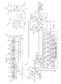
- Figure 3 illustrates an exemplary implementation of inverting delay element 12.
- Inverting delay elements 14, 16, 18, and 20 may be similarly constructed.
- Inverting delay element 12 includes inverter 40, programmable current sink 50, switch 52, and a shut off device 56.
- Inverter 40 is as described above in conjunction with Figure 2.
- Programmable current sink 50 comprises a plurality 58 of N-channel field effect transistors.
- Plurality 58 of N-channel field effect transistors includes field effect transistors 60, 62, 64, 66, 68, 70, 72, and 74.
- Plurality 58 of field effect transistors have sources connected to ground and drains connected a node 76.
- the gates of plurality 58 of transistors are connected to a plurality 77 of control nodes.
- Plurality 77 of control nodes includes control nodes 78, 80, 82, 84, 86, 88, 90, and 92.
- a transistor 94 serves as a switch 52 to selectively connect node 24 with node 76.
- Transistor 94 is an N-channel field effect transistor. The gate of transistor 94 is connected to shut-off device 56.
- a current source such as current source 51 is not utilized. Therefore, only charging of node 24 is delayed by robbing current from node 24.
- other embodiments of the invention could utilize a current source such as current source 51. Therefore, the delay period ⁇ of each inverting delay element 12, 14, 16, 18, and 20 will differ somewhat for transitions from low to high than for transitions from high to low.
- Shut-off device 56 includes a pair of inverters 94 and 96.
- Inverter 94 includes a P-channel field effect transistor 98 and an N-channel field effect transistor 100.
- the gates of P-channel field effect transistor 98 and N-channel field effect transistor are connected to a node 102.
- the drains of field effect transistors 98 and 100 are connected to an output node 104, which is connected to the gate of transistor 94 in switch 52. Therefore, the voltage at output node 104 of shut-off device 56 controls switch 52.
- Inverter 96 includes a P-channel field effect transistor 106 and an N-channel field effect transistor 108.
- the gates of P-channel field effect transistor 106 and N-channel field effect transistor 108 are connected to a node 110, which is connected to output node 26 of inverting delay element 14. Therefore, node 110 receives feedback signal 32 having the voltage at the output of the next inverting delay element, which in this example is inverting delay element 14.
- the drains of P-channel field effect transistor 106 and N-channel field effect transistor 108 are connected to node 112, which is connected to node 102.
- shut-off device 56 receives feedback signal 32 at node 110 from output node 26 of inverting delay element 14.
- Inverter 96 inverts the voltage at 110 and provides an output voltage at node 112, which is provided as an input voltage at node 102 to inverter 94.
- Inverter 94 inverts the voltage at node 102 to produce a voltage at node 104 that is the same as the voltage at node 26.
- the voltage at node 104 is provided to the gate of transistor 94 and therefore controls the status of switch 52. Because transistor 94 in switch 52 is an N-channel field effect transistor, a positive gate-to-source voltage of transistor 94 turns switch 52 on and a negative gate-to-source voltage turns switch 52 off.
- shut off device 56 includes inverters 94 and 96 rather than directly connecting the gate of transistor 94 to node 26 because of two reasons. The first is that inverter 96 may be a low strength inverter. Therefore inverter 96 does not provide a large load to the next stage. The second reason is that node 24 can completely transition before switch 52 is activated or deactivated.
- each transistor of the plurality of transistors 58 in programmable current sink 50 may be turned on or off to sink current by the application of an appropriate voltage at each of the plurality of control nodes 77. Because plurality 58 of field effect transistors are N-channel devices, a positive gate-to-source voltage applied to the gate of the transistors turns the transistors on. Thus, a maximum current may be sunk by programmable current sink 50 by applying a high voltage to each of the plurality of control nodes 77, and no voltage may be sunk by programmable current sink 50 by applying a low voltage to each of the plurality of control node 77.
- Varying amounts of current may be sunk by programmable current sink 50 by selectively controlling each of the plurality of control nodes 77.
- the current produced by transistors 60, 62, 64, 66, 68, 70, 72, and 74 are weighted such that the current produced by transistor 60 is k2 7 , the current produced by transistor 62 is k2 6 , the current produced by transistor 64 is k2 5 , the current produced by transistor 66 is k2 4 , the current produced by transistor 68 is k2 3 , the current produced by transistor 70 is k2 2 , the current produced by transistor 72 is k2 1 , the current produced by transistor 74 is k2 0 , where k is a constant.
- Control nodes 77 may therefore be controlled digitally by an 8 bit control word. Results of the operation of the above-described current-robbing oscillator 10 are described below in conjunction with Figure 4 through 6.
- Figure 4 is a graph of delay versus control word for current-robbing oscillator 10 for the four most-significant bits of the control word, which corresponds to control nodes 78, 80, 82, and 84.
- Each control word corresponds to a step change in current that is sunk by programmable current sink 50.
- the far left-hand side of FIGURE 4 corresponds to no current being sunk by programmable current sink 50 and the far right-hand side of FIGURE 5 corresponds to a large current being sunk by programmable current sink 50.
- the delay, or period, of current-robbing oscillator 10 is fairly linear with respect to the current sunk by programmable sink 50, as well as linear with respect to the control word.
- Figure 5 illustrates a graph of frequency of current-robbing oscillator 10 with respect to the control word, which corresponds to the amount of current sunk by programmable current sink 50.
- the relationship between frequency of current-robbing oscillator 10 and the control word is fairly linear over the range of 60 to 260 MHz, which is desirable.
- the linearity of the control region may be attributed to the robbing of current from output nodes of inverters in each delay element 12, 14, 16, 18, and 20, such as node 24 in inverter 40.
- the amount of current robbed from the inverter 40 is constant until a transition from a high to low voltage at node 24 is completed.
- oscillator 10 may produce an oscillating frequency with a higher frequency than traditional oscillators.
- Figure 6 illustrates a graph of current consumption for current-robbing oscillator 10 versus control word for the four most-significant bits of the control word, which corresponds to the amount of current sunk by programmable current sink 50.
- the far left hand side of the graph in FIGURE 6 corresponds to a control word of 0000, which represents no current sunk by programmable current sink 50
- the far right hand side of Figure 6 represents a control word of 1111, which corresponds to a large current sunk by programmable current sink 50.
- the current consumption of current-robbing oscillator 10 is highest when no current is sunk by programmable current source sink 50 and is lowest when the maximum amount of current is sunk by programmable current sink 50.
Landscapes
- Physics & Mathematics (AREA)
- Nonlinear Science (AREA)
- Pulse Circuits (AREA)
Applications Claiming Priority (2)
| Application Number | Priority Date | Filing Date | Title |
|---|---|---|---|
| US08/990,484 US5949292A (en) | 1997-12-15 | 1997-12-15 | Ring oscillator using current robbing for controlling delay period |
| US990484 | 1997-12-15 |
Publications (2)
| Publication Number | Publication Date |
|---|---|
| EP0926824A2 true EP0926824A2 (fr) | 1999-06-30 |
| EP0926824A3 EP0926824A3 (fr) | 2000-12-27 |
Family
ID=25536201
Family Applications (1)
| Application Number | Title | Priority Date | Filing Date |
|---|---|---|---|
| EP98309969A Withdrawn EP0926824A3 (fr) | 1997-12-15 | 1998-12-04 | Oscillateur à soustraction de courant et procédé correspondant |
Country Status (3)
| Country | Link |
|---|---|
| US (1) | US5949292A (fr) |
| EP (1) | EP0926824A3 (fr) |
| JP (2) | JPH11317647A (fr) |
Families Citing this family (16)
| Publication number | Priority date | Publication date | Assignee | Title |
|---|---|---|---|---|
| US5990714A (en) * | 1996-12-26 | 1999-11-23 | United Microelectronics Corporation | Clock signal generating circuit using variable delay circuit |
| JP2001339283A (ja) * | 2000-05-26 | 2001-12-07 | Mitsubishi Electric Corp | 遅延回路およびそのための半導体回路装置 |
| US6411150B1 (en) * | 2001-01-30 | 2002-06-25 | Cypress Semiconductor Corp. | Dynamic control of input buffer thresholds |
| JP2002261590A (ja) * | 2001-02-28 | 2002-09-13 | Asahi Kasei Microsystems Kk | 遅延装置 |
| US6509771B1 (en) | 2001-12-14 | 2003-01-21 | International Business Machines Corporation | Enhanced operational frequency for a precise and programmable duty cycle generator |
| US6577202B1 (en) | 2001-12-14 | 2003-06-10 | International Business Machines Corporation | Multiple duty cycle tap points for a precise and programmable duty cycle generator |
| US6603339B2 (en) | 2001-12-14 | 2003-08-05 | International Business Machines Corporation | Precision aligned multiple concurrent duty cycles from a programmable duty cycle generator |
| US6593789B2 (en) | 2001-12-14 | 2003-07-15 | International Business Machines Corporation | Precise and programmable duty cycle generator |
| US7212021B2 (en) * | 2002-03-12 | 2007-05-01 | Intel Corporation | Manufacturing integrated circuits and testing on-die power supplies using distributed programmable digital current sinks |
| US7039885B1 (en) * | 2003-01-21 | 2006-05-02 | Barcelona Design, Inc. | Methodology for design of oscillator delay stage and corresponding applications |
| GB2403082B (en) * | 2003-06-18 | 2005-08-31 | Motorola Inc | Arrangement and method for digital delay line |
| US20060224337A1 (en) * | 2005-03-31 | 2006-10-05 | Intel Corporation, A Delaware Corporation | Programmable current load systems and methods |
| KR100728996B1 (ko) | 2006-09-29 | 2007-06-15 | 주식회사 하이닉스반도체 | 링 오실레이터 |
| US10075133B2 (en) | 2016-01-15 | 2018-09-11 | Seamless Microsystems, Inc. | Systems and methods for ring-oscillator based operational amplifiers for scaled CMOS technologies |
| US10833664B2 (en) | 2017-08-14 | 2020-11-10 | Apple Inc. | Supply tracking delay element in multiple power domain designs |
| CN120567160B (zh) * | 2025-07-31 | 2025-10-03 | 中国人民解放军国防科技大学 | 利用相反时钟补偿加固的环形振荡器、芯片及电子设备 |
Citations (2)
| Publication number | Priority date | Publication date | Assignee | Title |
|---|---|---|---|---|
| JPH09191239A (ja) * | 1996-01-10 | 1997-07-22 | Hitachi Ltd | 可変遅延回路 |
| US5684423A (en) * | 1991-10-09 | 1997-11-04 | Fujitsu Limited | Variable delay circuit |
Family Cites Families (3)
| Publication number | Priority date | Publication date | Assignee | Title |
|---|---|---|---|---|
| US5300898A (en) * | 1992-07-29 | 1994-04-05 | Ncr Corporation | High speed current/voltage controlled ring oscillator circuit |
| JP3528203B2 (ja) * | 1993-06-30 | 2004-05-17 | ソニー株式会社 | リング発振器および電圧制御発振器 |
| US5559473A (en) * | 1994-06-23 | 1996-09-24 | At&T Global Information Solutions Company | Multi-range voltage controlled oscillator |
-
1997
- 1997-12-15 US US08/990,484 patent/US5949292A/en not_active Expired - Lifetime
-
1998
- 1998-12-04 EP EP98309969A patent/EP0926824A3/fr not_active Withdrawn
- 1998-12-15 JP JP10356489A patent/JPH11317647A/ja not_active Withdrawn
-
2008
- 2008-07-02 JP JP2008173522A patent/JP2008252943A/ja not_active Abandoned
Patent Citations (2)
| Publication number | Priority date | Publication date | Assignee | Title |
|---|---|---|---|---|
| US5684423A (en) * | 1991-10-09 | 1997-11-04 | Fujitsu Limited | Variable delay circuit |
| JPH09191239A (ja) * | 1996-01-10 | 1997-07-22 | Hitachi Ltd | 可変遅延回路 |
Also Published As
| Publication number | Publication date |
|---|---|
| EP0926824A3 (fr) | 2000-12-27 |
| JP2008252943A (ja) | 2008-10-16 |
| JPH11317647A (ja) | 1999-11-16 |
| US5949292A (en) | 1999-09-07 |
Similar Documents
| Publication | Publication Date | Title |
|---|---|---|
| JP2008252943A (ja) | 発振器 | |
| US5300898A (en) | High speed current/voltage controlled ring oscillator circuit | |
| US6191630B1 (en) | Delay circuit and oscillator circuit using same | |
| US4388537A (en) | Substrate bias generation circuit | |
| US5565817A (en) | Ring oscillator having accelerated charging and discharging of capacitors | |
| US4874971A (en) | Edge-sensitive dynamic switch | |
| US6346843B2 (en) | Clock signal generating circuit using variable delay circuit | |
| KR200156574Y1 (ko) | 가변 지연선 | |
| US7292079B2 (en) | DLL-based programmable clock generator using a threshold-trigger delay element circuit and a circular edge combiner | |
| JPH0158896B2 (fr) | ||
| US3995232A (en) | Integrated circuit oscillator | |
| US7471105B2 (en) | Level shifter and level shifting method for higher speed and lower power | |
| US6184754B1 (en) | Voltage-controlled oscillator circuit and voltage-controlled oscillating method | |
| KR100319505B1 (ko) | 집적회로 | |
| US6958626B2 (en) | Off chip driver | |
| US20130147564A1 (en) | Oscillator with frequency determined by relative magnitudes of current sources | |
| US5760655A (en) | Stable frequency oscillator having two capacitors that are alternately charged and discharged | |
| US6177846B1 (en) | Ring oscillator type voltage controlled oscillator | |
| US20030094978A1 (en) | Voltage-controlled oscillator having short synchronous pull-in time | |
| JPH0254698B2 (fr) | ||
| US20030218510A1 (en) | Self-regulating voltage controlled oscillator | |
| US5801566A (en) | System clock generating circuit for a semiconductor device | |
| JP3611045B2 (ja) | 位相整合回路 | |
| US20060170478A1 (en) | Delay circuit for semiconductor device | |
| JPH07336216A (ja) | 電圧制御発振器 |
Legal Events
| Date | Code | Title | Description |
|---|---|---|---|
| PUAI | Public reference made under article 153(3) epc to a published international application that has entered the european phase |
Free format text: ORIGINAL CODE: 0009012 |
|
| AK | Designated contracting states |
Kind code of ref document: A2 Designated state(s): DE FR GB IT NL |
|
| AX | Request for extension of the european patent |
Free format text: AL;LT;LV;MK;RO;SI |
|
| RIN1 | Information on inventor provided before grant (corrected) |
Inventor name: TAYLOR, LUNDY (NMI) Inventor name: DONDERSHINE, STEVEN L. Inventor name: FAHRENBRUCH, SHAWN A. |
|
| PUAL | Search report despatched |
Free format text: ORIGINAL CODE: 0009013 |
|
| AK | Designated contracting states |
Kind code of ref document: A3 Designated state(s): AT BE CH CY DE DK ES FI FR GB GR IE IT LI LU MC NL PT SE |
|
| AX | Request for extension of the european patent |
Free format text: AL;LT;LV;MK;RO;SI |
|
| 17P | Request for examination filed |
Effective date: 20010516 |
|
| AKX | Designation fees paid |
Free format text: DE FR GB IT NL |
|
| 17Q | First examination report despatched |
Effective date: 20020823 |
|
| STAA | Information on the status of an ep patent application or granted ep patent |
Free format text: STATUS: THE APPLICATION IS DEEMED TO BE WITHDRAWN |
|
| 18D | Application deemed to be withdrawn |
Effective date: 20030103 |