EP0930701A2 - Filtre stratifié - Google Patents
Filtre stratifié Download PDFInfo
- Publication number
- EP0930701A2 EP0930701A2 EP99100880A EP99100880A EP0930701A2 EP 0930701 A2 EP0930701 A2 EP 0930701A2 EP 99100880 A EP99100880 A EP 99100880A EP 99100880 A EP99100880 A EP 99100880A EP 0930701 A2 EP0930701 A2 EP 0930701A2
- Authority
- EP
- European Patent Office
- Prior art keywords
- electrode
- disposed
- resonator
- input
- electrodes
- Prior art date
- Legal status (The legal status is an assumption and is not a legal conclusion. Google has not performed a legal analysis and makes no representation as to the accuracy of the status listed.)
- Granted
Links
Images

Classifications
-
- H—ELECTRICITY
- H01—ELECTRIC ELEMENTS
- H01P—WAVEGUIDES; RESONATORS, LINES, OR OTHER DEVICES OF THE WAVEGUIDE TYPE
- H01P1/00—Auxiliary devices
- H01P1/20—Frequency-selective devices, e.g. filters
- H01P1/201—Filters for transverse electromagnetic waves
- H01P1/205—Comb or interdigital filters; Cascaded coaxial cavities
-
- H—ELECTRICITY
- H03—ELECTRONIC CIRCUITRY
- H03H—IMPEDANCE NETWORKS, e.g. RESONANT CIRCUITS; RESONATORS
- H03H9/00—Networks comprising electromechanical or electro-acoustic elements; Electromechanical resonators
- H03H9/02—Details
- H03H9/05—Holders or supports
- H03H9/10—Mounting in enclosures
- H03H9/1007—Mounting in enclosures for bulk acoustic wave [BAW] devices
- H03H9/1035—Mounting in enclosures for bulk acoustic wave [BAW] devices the enclosure being defined by two sealing substrates sandwiching the piezoelectric layer of the BAW device
-
- H—ELECTRICITY
- H01—ELECTRIC ELEMENTS
- H01P—WAVEGUIDES; RESONATORS, LINES, OR OTHER DEVICES OF THE WAVEGUIDE TYPE
- H01P1/00—Auxiliary devices
- H01P1/20—Frequency-selective devices, e.g. filters
- H01P1/201—Filters for transverse electromagnetic waves
- H01P1/203—Strip line filters
- H01P1/20327—Electromagnetic interstage coupling
- H01P1/20336—Comb or interdigital filters
- H01P1/20345—Multilayer filters
-
- H—ELECTRICITY
- H01—ELECTRIC ELEMENTS
- H01P—WAVEGUIDES; RESONATORS, LINES, OR OTHER DEVICES OF THE WAVEGUIDE TYPE
- H01P7/00—Resonators of the waveguide type
- H01P7/10—Dielectric resonators
-
- H—ELECTRICITY
- H03—ELECTRONIC CIRCUITRY
- H03H—IMPEDANCE NETWORKS, e.g. RESONANT CIRCUITS; RESONATORS
- H03H9/00—Networks comprising electromechanical or electro-acoustic elements; Electromechanical resonators
- H03H9/02—Details
- H03H9/05—Holders or supports
- H03H9/0538—Constructional combinations of supports or holders with electromechanical or other electronic elements
- H03H9/0547—Constructional combinations of supports or holders with electromechanical or other electronic elements consisting of a vertical arrangement
- H03H9/0561—Constructional combinations of supports or holders with electromechanical or other electronic elements consisting of a vertical arrangement consisting of a multilayered structure
Definitions
- the present invention relates to the field of laminated filters used for products such as communications equipment.
- laminated filters are configured by providing resonator electrodes in parallel on an inner layer within a stack of several laminated dielectric sheets, and an I/O electrode at a position facing the resonator electrodes through this inner layer of the dielectric sheets.
- another resonator electrode and capacitance are connected in series to form a resonator electrode for notching, and connected to the laminated filter.
- This resonator electrode for notching generates an attenuation pole within the frequency characteristics, steepening the frequency characteristics curve.
- a laminated filter of the present invention comprises a laminated body created by laminating a plurality of dielectric sheets, a plurality of resonator electrodes disposed on the same layer within an inner part of the laminated body, and a first input-output electrode disposed on the inner part of the laminated body at a position facing one of the resonator electrodes for input through the dielectric sheet, a second input-output electrode disposed on the inner part of the laminated body at a position facing one of the resonator electrodes for output through the dielectric sheet.
- One end of at least one of the first and second input-output electrodes is connected to a stub electrode which has one open-circuit end.
- the stub electrodes By connecting the stub electrodes to the I/O electrodes, a large attenuation is achieved and, at the same time, the size of the laminated filter can be reduced.
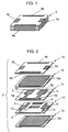
- a laminated filter in a preferred embodiment of the present invention is explained with reference to Figs. 1 to 4.
- dielectric sheets 1a to 1e are made of generally rectangular ceramic dielectric sheets but other shapes may be used. These dielectric sheets 1a to 1e are laminated together to form laminated body 2 including a plurality of inner dielectric sheets 1b, 1c and 1d forming an inner part.
- Input-output (I/O) terminals 3a and 3b and ground terminals 4a and 4b are disposed, as shown in Fig. 1, at the side faces of the laminated body 2.
- the I/O terminals 3a and 3b are disposed on opposed side faces.
- One of two resonator electrodes 5 forms part of an input resonance circuit, and the other forms part of an output resonance circuit. These two resonator electrodes 5 are disposed on dielectric sheet 1c. For each resonator electrode 5, one end is connected to the ground terminal 4a, forming a short-circuit end 5a, and the other end extends towards ground terminal 4b and forms an open-circuit end 5b.
- I/O electrodes 6 are disposed on dielectric sheet 1d. One end of each I/O electrode 6 is connected to a corresponding I/O terminal 3a or 3b. The other end of each I/O electrode 6 is located at a position facing the open-circuit end 5b of one of the resonator electrodes 5 for input and output through the dielectric sheet 1c, forming input-output (I/O) capacitance 7 shown in Fig. 3.
- a coupling electrode 8 is disposed on dielectric sheet 1d. Coupling electrode 8 is disposed facing portions of both resonator electrodes 5which are placed side by side, and through the dielectric sheet 1c, creating an inter-stage coupling capacitance 9 shown in Fig. 3.
- a frequency compression electrode 10 is disposed on the dielectric sheet 1d. One end of the frequency compression electrode 10 is connected to the ground terminal 4b, and the other end is disposed at a position facing the open-circuit end 5b of the resonator electrode 5 through the dielectric sheet 1c, creating a loading capacitance 11 shown in Fig. 3.
- Shielding electrode 12a is disposed on dielectric sheet 1b on top of the dielectric sheet 1c and shielding electrode 12d is disposed on the dielectric sheet 1e underneath the dielectric sheet 1d, respectively.
- Shielding electrodes 12a and 12b are respectively connected to the ground terminals 4a and 4b.
- the purpose of these shielding electrodes 12a and 12b on the upper face of the topmost inner layer and the bottom layer of the laminated filter is to vertically sandwich the components of a filter circuit disposed on an inner part of the laminated body 2, i.e., the resonator electrodes 5, I/O electrodes 6, frequency compression electrode 10, stub electrode or electrodes 13, and coupling electrode 8; so as to improve the shielding capability of the laminated filter.
- Each stub electrode 13 includes a strip disposed on the dielectric sheet 1d at a position which does not overlap any portion of the resonator electrode 5 through the dielectric sheet 1c. One end of each stub electrode 13 is connected to an I/O electrode 6, and the other end is an open-circuit end.
- Each stub electrode 13 is a 1/4-wavelength strip line.
- impedance at the open-circuit end becomes 0.
- these signals are short-circuited, generating attenuation pole 14 within the frequency characteristics as shown in the attenuation - frequency curve shown in Fig. 4.
- the laminated filter of the present invention can be made smaller.
- the laminated filter demonstrates high performance.
- each stub electrode 13 is connected to an I/O electrode 6, and the other end is extended toward the short-circuit end 5a of the resonator electrode 5. If, however, the stub electrode 13 were to extend toward the open-circuit end 5b of a corresponding resonator electrode 5 and were disposed facing resonator electrode 5 across dielectric sheet 1c, the stub electrode 13 would form a capacitance coupling with the resonator electrode 5 across dielectric sheet 1c because the open-circuit end 5b of the resonator electrode 5 has a strong capacitance coupling capability. This will prevent generation of the attenuation pole 14 shown in Fig. 4, resulting in the formation of only I/O capacitance 7 shown in Fig. 3.
- the laminated filter of the present invention secures a larger attenuation and prevents capacitance coupling between the stub electrode and the resonator electrode by connecting the stub electrode to the I/O electrode. Accordingly, the present invention enables the required frequency characteristics to be achieved and also provides for a smaller-sized laminated filter.
- the preferred embodiment of the present invention is explained in details with reference to the case when a dielectric sheet on which a resonator electrode is formed and a dielectric sheet on which an I/O electrode is formed are laminated adjacent each other.
- the invention may be practiced or embodied in still other combinations.
- another dielectric sheet may be disposed between these two dielectric sheets (which are dielectric sheets shown as sheets 1c and 1d as shown in Fig. 2).
- the essential characteristic of the invention is that the resonator electrode and I/O electrode are facing each other through a dielectric sheet or sheets.
- the preferred embodiment described herein is therefore illustrative and not restrictive.
- the scope of the invention is indicated by the appended claims and all modifications which come within the true spirit of the claims are intended to be embraced therein.
Landscapes
- Physics & Mathematics (AREA)
- Electromagnetism (AREA)
- Acoustics & Sound (AREA)
- Control Of Motors That Do Not Use Commutators (AREA)
Applications Claiming Priority (2)
| Application Number | Priority Date | Filing Date | Title |
|---|---|---|---|
| JP10008313A JPH11205006A (ja) | 1998-01-20 | 1998-01-20 | 積層フィルタ |
| JP831398 | 1998-01-20 |
Publications (3)
| Publication Number | Publication Date |
|---|---|
| EP0930701A2 true EP0930701A2 (fr) | 1999-07-21 |
| EP0930701A3 EP0930701A3 (fr) | 2001-06-06 |
| EP0930701B1 EP0930701B1 (fr) | 2006-04-05 |
Family
ID=11689676
Family Applications (1)
| Application Number | Title | Priority Date | Filing Date |
|---|---|---|---|
| EP99100880A Expired - Lifetime EP0930701B1 (fr) | 1998-01-20 | 1999-01-19 | Filtre stratifié |
Country Status (5)
| Country | Link |
|---|---|
| US (1) | US6191669B1 (fr) |
| EP (1) | EP0930701B1 (fr) |
| JP (1) | JPH11205006A (fr) |
| KR (1) | KR100462698B1 (fr) |
| DE (1) | DE69930680T2 (fr) |
Cited By (1)
| Publication number | Priority date | Publication date | Assignee | Title |
|---|---|---|---|---|
| EP1988598A3 (fr) * | 2007-05-02 | 2009-09-02 | NGK Sparkplug Co., Ltd. | Filtre de bande passante stratifié et diplexeur l'utilisant |
Families Citing this family (52)
| Publication number | Priority date | Publication date | Assignee | Title |
|---|---|---|---|---|
| US7274549B2 (en) | 2000-12-15 | 2007-09-25 | X2Y Attenuators, Llc | Energy pathway arrangements for energy conditioning |
| US9054094B2 (en) | 1997-04-08 | 2015-06-09 | X2Y Attenuators, Llc | Energy conditioning circuit arrangement for integrated circuit |
| US7042703B2 (en) | 2000-03-22 | 2006-05-09 | X2Y Attenuators, Llc | Energy conditioning structure |
| US7110235B2 (en) | 1997-04-08 | 2006-09-19 | Xzy Altenuators, Llc | Arrangement for energy conditioning |
| US6606011B2 (en) | 1998-04-07 | 2003-08-12 | X2Y Attenuators, Llc | Energy conditioning circuit assembly |
| WO1999052210A1 (fr) | 1998-04-07 | 1999-10-14 | X2Y Attenuators, L.L.C. | Support de composants |
| US7301748B2 (en) | 1997-04-08 | 2007-11-27 | Anthony Anthony A | Universal energy conditioning interposer with circuit architecture |
| US7336467B2 (en) | 2000-10-17 | 2008-02-26 | X2Y Attenuators, Llc | Energy pathway arrangement |
| US6894884B2 (en) | 1997-04-08 | 2005-05-17 | Xzy Attenuators, Llc | Offset pathway arrangements for energy conditioning |
| US6650525B2 (en) | 1997-04-08 | 2003-11-18 | X2Y Attenuators, Llc | Component carrier |
| US6018448A (en) | 1997-04-08 | 2000-01-25 | X2Y Attenuators, L.L.C. | Paired multi-layered dielectric independent passive component architecture resulting in differential and common mode filtering with surge protection in one integrated package |
| US20030161086A1 (en) | 2000-07-18 | 2003-08-28 | X2Y Attenuators, Llc | Paired multi-layered dielectric independent passive component architecture resulting in differential and common mode filtering with surge protection in one integrated package |
| US7321485B2 (en) | 1997-04-08 | 2008-01-22 | X2Y Attenuators, Llc | Arrangement for energy conditioning |
| US7106570B2 (en) | 1997-04-08 | 2006-09-12 | Xzy Altenuators, Llc | Pathway arrangement |
| US7336468B2 (en) | 1997-04-08 | 2008-02-26 | X2Y Attenuators, Llc | Arrangement for energy conditioning |
| US7110227B2 (en) | 1997-04-08 | 2006-09-19 | X2Y Attenuators, Llc | Universial energy conditioning interposer with circuit architecture |
| US6954346B2 (en) | 1997-04-08 | 2005-10-11 | Xzy Attenuators, Llc | Filter assembly |
| US6603646B2 (en) * | 1997-04-08 | 2003-08-05 | X2Y Attenuators, Llc | Multi-functional energy conditioner |
| US7427816B2 (en) | 1998-04-07 | 2008-09-23 | X2Y Attenuators, Llc | Component carrier |
| EP1067618B1 (fr) * | 1999-07-08 | 2007-12-12 | Matsushita Electric Industrial Co., Ltd. | Filtre stratifié, duplexeur et dispositif de communication mobile l' utilisant |
| US7113383B2 (en) | 2000-04-28 | 2006-09-26 | X2Y Attenuators, Llc | Predetermined symmetrically balanced amalgam with complementary paired portions comprising shielding electrodes and shielded electrodes and other predetermined element portions for symmetrically balanced and complementary energy portion conditioning |
| EP1312148A4 (fr) | 2000-08-15 | 2009-06-03 | X2Y Attenuators Llc | Systeme d'electrodes pour conditionnement d'energie en circuit |
| US7193831B2 (en) * | 2000-10-17 | 2007-03-20 | X2Y Attenuators, Llc | Energy pathway arrangement |
| KR100536511B1 (ko) * | 2000-10-17 | 2005-12-14 | 엑스2와이 어테뉴에이터스, 엘.엘.씨 | 공통 기준 노드를 갖는 단일 또는 다수의 회로들을 위한 차폐 아말감 및 차폐된 에너지 경로들 및 다른 엘리먼트들 |
| WO2002047936A1 (fr) * | 2000-12-12 | 2002-06-20 | Japan Science And Technology Corporation | Mecanisme de direction pour voiture electrique |
| US20020158305A1 (en) * | 2001-01-05 | 2002-10-31 | Sidharth Dalmia | Organic substrate having integrated passive components |
| EP1384302A1 (fr) * | 2001-04-02 | 2004-01-28 | X2Y Attenuators, L.L.C. | Ensembles de chemins decales pour conditionnement d'energie |
| KR100432846B1 (ko) * | 2001-05-10 | 2004-05-24 | 전자부품연구원 | 자계 결합 세기의 조절가능한 적층형 유전체 필터 |
| KR100430253B1 (ko) * | 2002-05-10 | 2004-05-03 | 엘지이노텍 주식회사 | 스트립 라인을 이용한 필터회로 제조방법 |
| KR20030092443A (ko) * | 2002-05-29 | 2003-12-06 | 엘지이노텍 주식회사 | 고주파용 대역통과필터 |
| US6900708B2 (en) * | 2002-06-26 | 2005-05-31 | Georgia Tech Research Corporation | Integrated passive devices fabricated utilizing multi-layer, organic laminates |
| US7260890B2 (en) * | 2002-06-26 | 2007-08-28 | Georgia Tech Research Corporation | Methods for fabricating three-dimensional all organic interconnect structures |
| US6987307B2 (en) * | 2002-06-26 | 2006-01-17 | Georgia Tech Research Corporation | Stand-alone organic-based passive devices |
| US7180718B2 (en) * | 2003-01-31 | 2007-02-20 | X2Y Attenuators, Llc | Shielded energy conditioner |
| US7489914B2 (en) * | 2003-03-28 | 2009-02-10 | Georgia Tech Research Corporation | Multi-band RF transceiver with passive reuse in organic substrates |
| WO2005002018A2 (fr) | 2003-05-29 | 2005-01-06 | X2Y Attenuators, Llc | Connecteur se rapportant a des structures comprenant un conditionneur d'energie |
| KR20060120683A (ko) | 2003-12-22 | 2006-11-27 | 엑스2와이 어테뉴에이터스, 엘.엘.씨 | 내부적으로 차폐된 에너지 컨디셔너 |
| US8345433B2 (en) * | 2004-07-08 | 2013-01-01 | Avx Corporation | Heterogeneous organic laminate stack ups for high frequency applications |
| US20060077020A1 (en) * | 2004-10-13 | 2006-04-13 | Cyntec Company | Circuits and manufacturing configurations of compact band-pass filter |
| JP2008537843A (ja) | 2005-03-01 | 2008-09-25 | エックストゥーワイ アテニュエイターズ,エルエルシー | 内部で重なり合った調整器 |
| WO2006093831A2 (fr) | 2005-03-01 | 2006-09-08 | X2Y Attenuators, Llc | Conditionneur d'energie avec electrodes traversantes reliees |
| WO2006099297A2 (fr) | 2005-03-14 | 2006-09-21 | X2Y Attenuators, Llc | Conditionneur a conducteurs coplanaires |
| EP1991996A1 (fr) | 2006-03-07 | 2008-11-19 | X2Y Attenuators, L.L.C. | Structures de conditionneur d'énergie |
| US7439840B2 (en) | 2006-06-27 | 2008-10-21 | Jacket Micro Devices, Inc. | Methods and apparatuses for high-performing multi-layer inductors |
| US7808434B2 (en) * | 2006-08-09 | 2010-10-05 | Avx Corporation | Systems and methods for integrated antennae structures in multilayer organic-based printed circuit devices |
| US7989895B2 (en) | 2006-11-15 | 2011-08-02 | Avx Corporation | Integration using package stacking with multi-layer organic substrates |
| JP5633708B2 (ja) * | 2012-04-05 | 2014-12-03 | Tdk株式会社 | 積層型バンドパスフィルタ |
| KR101431005B1 (ko) * | 2012-05-31 | 2014-08-20 | 주식회사 릿치마이크로웨이브 | 3차원 적층 유전체 공진기 조립체 |
| KR101333165B1 (ko) * | 2013-07-11 | 2013-11-27 | 주식회사 티에프티 | 변압기용 불연성 부싱 및 그 제조방법 |
| KR101672902B1 (ko) | 2016-06-02 | 2016-11-07 | 우진전기 주식회사 | 변압기용 리드선 일체형 고압 복합부싱 |
| KR101642765B1 (ko) | 2016-06-02 | 2016-07-27 | 우진전기 주식회사 | 리드선 일체형 고압 복합부싱이 설치된 주상변압기 |
| US11682816B2 (en) * | 2019-08-22 | 2023-06-20 | Mediatek Inc. | Filter circuits |
Family Cites Families (9)
| Publication number | Priority date | Publication date | Assignee | Title |
|---|---|---|---|---|
| JP3115149B2 (ja) * | 1993-03-31 | 2000-12-04 | 日本碍子株式会社 | 積層型誘電体フィルタ |
| EP0917235B1 (fr) * | 1993-08-24 | 2003-01-22 | Matsushita Electric Industrial Co., Ltd. | Duplexeur diélectrique stratifié d' antenne |
| JP3509820B2 (ja) * | 1994-07-08 | 2004-03-22 | 宇部興産株式会社 | ストリップライン型フィルタ |
| JP3558696B2 (ja) * | 1994-08-26 | 2004-08-25 | 日本無線株式会社 | 積層誘電体フィルタ |
| JPH08213805A (ja) * | 1995-02-03 | 1996-08-20 | Matsushita Electric Ind Co Ltd | 積層フィルタ |
| JP3050103B2 (ja) * | 1995-10-19 | 2000-06-12 | 松下電器産業株式会社 | 積層フィルタとそれを用いたフィルタ装置 |
| US5892415A (en) * | 1995-11-20 | 1999-04-06 | Murata Manufacturing Co., Ltd. | Laminated resonator and laminated band pass filter using same |
| JPH09153703A (ja) * | 1995-11-28 | 1997-06-10 | Hitachi Metals Ltd | 誘電体積層フィルタ |
| EP0837517B1 (fr) * | 1996-10-18 | 2004-01-28 | Matsushita Electric Industrial Co., Ltd. | Filtre diélectrique statifié et dispositif de communication |
-
1998
- 1998-01-20 JP JP10008313A patent/JPH11205006A/ja active Pending
-
1999
- 1999-01-16 KR KR10-1999-0004322A patent/KR100462698B1/ko not_active Expired - Fee Related
- 1999-01-19 EP EP99100880A patent/EP0930701B1/fr not_active Expired - Lifetime
- 1999-01-19 DE DE69930680T patent/DE69930680T2/de not_active Expired - Fee Related
- 1999-01-20 US US09/233,512 patent/US6191669B1/en not_active Expired - Fee Related
Cited By (2)
| Publication number | Priority date | Publication date | Assignee | Title |
|---|---|---|---|---|
| EP1988598A3 (fr) * | 2007-05-02 | 2009-09-02 | NGK Sparkplug Co., Ltd. | Filtre de bande passante stratifié et diplexeur l'utilisant |
| US7902941B2 (en) | 2007-05-02 | 2011-03-08 | Ngk Spark Plug Co., Ltd. | Laminate type band pass filter and diplexer using the same |
Also Published As
| Publication number | Publication date |
|---|---|
| DE69930680T2 (de) | 2006-08-24 |
| JPH11205006A (ja) | 1999-07-30 |
| KR19990068244A (ko) | 1999-08-25 |
| EP0930701A3 (fr) | 2001-06-06 |
| DE69930680D1 (de) | 2006-05-18 |
| EP0930701B1 (fr) | 2006-04-05 |
| KR100462698B1 (ko) | 2004-12-20 |
| US6191669B1 (en) | 2001-02-20 |
Similar Documents
| Publication | Publication Date | Title |
|---|---|---|
| US6191669B1 (en) | Laminated filter | |
| EP0917232B1 (fr) | Filtre diélectrique stratifié | |
| US7116188B2 (en) | Laminated dielectric filter, and antenna duplexer and communication equipment using the same | |
| US5777533A (en) | LC filter with external electrodes only on a smaller layer | |
| EP1050962A1 (fr) | Filtre d'ondes acoustiques de surface | |
| JPH03262313A (ja) | バンドパスフィルタ | |
| KR970031264A (ko) | 적층형 공진기 및 이를 이용한 적층형 대역 필터(Laminated Resonator and Laminated Band Pass Filter Using Same) | |
| US6414568B1 (en) | Interdigitated, laminated LC bandpass filter with different length electrodes | |
| JP2957573B1 (ja) | 積層型フィルタ | |
| US5214398A (en) | Dielectric filter coupling structure having a compact terminal arrangement | |
| US5977848A (en) | Polar dielectric filter and dielectric duplexer incorporating same | |
| JPH06151243A (ja) | 積層型フィルタ | |
| JPH10117104A (ja) | 積層誘電体フィルタ | |
| US20020101305A1 (en) | Band pass filter | |
| JP3425065B2 (ja) | 積層型誘電体フィルタ | |
| JP2710904B2 (ja) | 積層型誘電体フィルタ | |
| JPH05335804A (ja) | 積層型誘電体フィルタ | |
| JP3191560B2 (ja) | 共振器およびフィルタ | |
| JPH04220001A (ja) | 誘電体フィルタ | |
| JPH11136001A (ja) | 周波数特性が改善された積層型ストリップライン・フィルタ | |
| JPS60100802A (ja) | 分布定数型フイルタ | |
| JPH11186808A (ja) | 積層フィルタ | |
| JPH0923102A (ja) | フィルター | |
| JP2004140878A (ja) | 積層型誘電体フィルタ | |
| JPH11195901A (ja) | 積層フィルタ |
Legal Events
| Date | Code | Title | Description |
|---|---|---|---|
| PUAI | Public reference made under article 153(3) epc to a published international application that has entered the european phase |
Free format text: ORIGINAL CODE: 0009012 |
|
| AK | Designated contracting states |
Kind code of ref document: A2 Designated state(s): DE FR GB |
|
| AX | Request for extension of the european patent |
Free format text: AL;LT;LV;MK;RO;SI |
|
| PUAL | Search report despatched |
Free format text: ORIGINAL CODE: 0009013 |
|
| AK | Designated contracting states |
Kind code of ref document: A3 Designated state(s): AT BE CH CY DE DK ES FI FR GB GR IE IT LI LU MC NL PT SE |
|
| AX | Request for extension of the european patent |
Free format text: AL;LT;LV;MK;RO;SI |
|
| RIC1 | Information provided on ipc code assigned before grant |
Free format text: 7H 01P 1/203 A |
|
| 17P | Request for examination filed |
Effective date: 20011002 |
|
| AKX | Designation fees paid |
Free format text: DE FR GB |
|
| 17Q | First examination report despatched |
Effective date: 20040511 |
|
| GRAP | Despatch of communication of intention to grant a patent |
Free format text: ORIGINAL CODE: EPIDOSNIGR1 |
|
| GRAS | Grant fee paid |
Free format text: ORIGINAL CODE: EPIDOSNIGR3 |
|
| GRAA | (expected) grant |
Free format text: ORIGINAL CODE: 0009210 |
|
| AK | Designated contracting states |
Kind code of ref document: B1 Designated state(s): DE FR GB |
|
| REG | Reference to a national code |
Ref country code: GB Ref legal event code: FG4D |
|
| REF | Corresponds to: |
Ref document number: 69930680 Country of ref document: DE Date of ref document: 20060518 Kind code of ref document: P |
|
| ET | Fr: translation filed | ||
| PLBE | No opposition filed within time limit |
Free format text: ORIGINAL CODE: 0009261 |
|
| STAA | Information on the status of an ep patent application or granted ep patent |
Free format text: STATUS: NO OPPOSITION FILED WITHIN TIME LIMIT |
|
| 26N | No opposition filed |
Effective date: 20070108 |
|
| PGFP | Annual fee paid to national office [announced via postgrant information from national office to epo] |
Ref country code: GB Payment date: 20080116 Year of fee payment: 10 Ref country code: DE Payment date: 20080117 Year of fee payment: 10 |
|
| PGFP | Annual fee paid to national office [announced via postgrant information from national office to epo] |
Ref country code: FR Payment date: 20080108 Year of fee payment: 10 |
|
| GBPC | Gb: european patent ceased through non-payment of renewal fee |
Effective date: 20090119 |
|
| PG25 | Lapsed in a contracting state [announced via postgrant information from national office to epo] |
Ref country code: DE Free format text: LAPSE BECAUSE OF NON-PAYMENT OF DUE FEES Effective date: 20090801 |
|
| REG | Reference to a national code |
Ref country code: FR Ref legal event code: ST Effective date: 20091030 |
|
| PG25 | Lapsed in a contracting state [announced via postgrant information from national office to epo] |
Ref country code: GB Free format text: LAPSE BECAUSE OF NON-PAYMENT OF DUE FEES Effective date: 20090119 |
|
| PG25 | Lapsed in a contracting state [announced via postgrant information from national office to epo] |
Ref country code: FR Free format text: LAPSE BECAUSE OF NON-PAYMENT OF DUE FEES Effective date: 20090202 |