EP0935280A1 - SOI Substrat und dessen Herstellungsverfahren - Google Patents
SOI Substrat und dessen Herstellungsverfahren Download PDFInfo
- Publication number
- EP0935280A1 EP0935280A1 EP99300620A EP99300620A EP0935280A1 EP 0935280 A1 EP0935280 A1 EP 0935280A1 EP 99300620 A EP99300620 A EP 99300620A EP 99300620 A EP99300620 A EP 99300620A EP 0935280 A1 EP0935280 A1 EP 0935280A1
- Authority
- EP
- European Patent Office
- Prior art keywords
- outer peripheral
- layer
- semiconductor
- insulation layer
- semiconductor substrate
- Prior art date
- Legal status (The legal status is an assumption and is not a legal conclusion. Google has not performed a legal analysis and makes no representation as to the accuracy of the status listed.)
- Granted
Links
Images


Classifications
-
- H—ELECTRICITY
- H10—SEMICONDUCTOR DEVICES; ELECTRIC SOLID-STATE DEVICES NOT OTHERWISE PROVIDED FOR
- H10P—GENERIC PROCESSES OR APPARATUS FOR THE MANUFACTURE OR TREATMENT OF DEVICES COVERED BY CLASS H10
- H10P95/00—Generic processes or apparatus for manufacture or treatments not covered by the other groups of this subclass
-
- H—ELECTRICITY
- H10—SEMICONDUCTOR DEVICES; ELECTRIC SOLID-STATE DEVICES NOT OTHERWISE PROVIDED FOR
- H10P—GENERIC PROCESSES OR APPARATUS FOR THE MANUFACTURE OR TREATMENT OF DEVICES COVERED BY CLASS H10
- H10P90/00—Preparation of wafers not covered by a single main group of this subclass, e.g. wafer reinforcement
- H10P90/19—Preparing inhomogeneous wafers
- H10P90/1904—Preparing vertically inhomogeneous wafers
- H10P90/1906—Preparing SOI wafers
- H10P90/1914—Preparing SOI wafers using bonding
-
- H—ELECTRICITY
- H10—SEMICONDUCTOR DEVICES; ELECTRIC SOLID-STATE DEVICES NOT OTHERWISE PROVIDED FOR
- H10W—GENERIC PACKAGES, INTERCONNECTIONS, CONNECTORS OR OTHER CONSTRUCTIONAL DETAILS OF DEVICES COVERED BY CLASS H10
- H10W10/00—Isolation regions in semiconductor bodies between components of integrated devices
- H10W10/10—Isolation regions comprising dielectric materials
- H10W10/181—Semiconductor-on-insulator [SOI] isolation regions, e.g. buried oxide regions of SOI wafers
-
- Y—GENERAL TAGGING OF NEW TECHNOLOGICAL DEVELOPMENTS; GENERAL TAGGING OF CROSS-SECTIONAL TECHNOLOGIES SPANNING OVER SEVERAL SECTIONS OF THE IPC; TECHNICAL SUBJECTS COVERED BY FORMER USPC CROSS-REFERENCE ART COLLECTIONS [XRACs] AND DIGESTS
- Y10—TECHNICAL SUBJECTS COVERED BY FORMER USPC
- Y10T—TECHNICAL SUBJECTS COVERED BY FORMER US CLASSIFICATION
- Y10T156/00—Adhesive bonding and miscellaneous chemical manufacture
- Y10T156/10—Methods of surface bonding and/or assembly therefor
- Y10T156/1002—Methods of surface bonding and/or assembly therefor with permanent bending or reshaping or surface deformation of self sustaining lamina
- Y10T156/1043—Subsequent to assembly
-
- Y—GENERAL TAGGING OF NEW TECHNOLOGICAL DEVELOPMENTS; GENERAL TAGGING OF CROSS-SECTIONAL TECHNOLOGIES SPANNING OVER SEVERAL SECTIONS OF THE IPC; TECHNICAL SUBJECTS COVERED BY FORMER USPC CROSS-REFERENCE ART COLLECTIONS [XRACs] AND DIGESTS
- Y10—TECHNICAL SUBJECTS COVERED BY FORMER USPC
- Y10T—TECHNICAL SUBJECTS COVERED BY FORMER US CLASSIFICATION
- Y10T156/00—Adhesive bonding and miscellaneous chemical manufacture
- Y10T156/10—Methods of surface bonding and/or assembly therefor
- Y10T156/1052—Methods of surface bonding and/or assembly therefor with cutting, punching, tearing or severing
Definitions
- This invention relates to a semiconductor substrate comprising a semiconductor layer arranged on a supporting base member and also to a method of manufacturing such a semiconductor substrate.
- SOI semiconductor on insulator
- the SOI technology can go back to the days of the SOS (silicon on sapphire) technology of forming an Si layer on a single crystal sapphire substrate by means of hetero-epitaxial growth, using a CVD (chemical vapor phase growth) method.
- SOS silicon on sapphire
- CVD chemical vapor phase growth
- the SIMOX (separation by ion implanted oxygen) technology followed the SOS technology.
- the methods known to date other than the SIMOX technology include a method of bonding a pair of wafers with an oxide film interposed therebetween and polishing or etching one of the wafers to leave a thin single crystal Si layer on the oxide film, a method of implanting hydrogen ions from the surface of an Si substrate carrying thereon an oxide film to a predetermined depth, bonding the substrate to another substrate and then peeling off the latter substrate with a thin single crystal Si layer left on the oxide film typically by means of heat treatment.
- the strength of bonding the silicon substrates can be reduced and even nullified in the peripheral area as it is adversely affected typically by the operation of beveling the substrates.
- SOI wafers under such conditions can become chipped in areas where the bonding strength is not sufficient and the surfaces of the wafers can become damaged, if partly, by Si debris in the course of manufacturing semiconductor devices to reduce the yield of manufacturing high quality semiconductor devices.
- Japanese Patent No. 2658135 discloses a technique for preventing a chipping phenomenon from occurring in a semiconductor substrate comprising a semiconductor layer arranged on a support member by mechanically grinding the outer peripheral edge of the support member by means of a wheel having a electrodeposition surface of diamond.
- highly integrated high-density semiconductor devices require further preventive measures for preventing the appearance of fine debris.
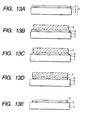
- FIGS. 13A through 13E of the accompanying drawings schematically illustrate a silicon removing process proposed by the inventors of the present invention.
- FIG. 13A shows an SOI substrate 5 prepared by bonding and etching-back operations and comprising an insulation film 2 and a thinned silicon layer 3 that are formed on a support member 1.
- An outer peripheral portion of the silicon layer 3 of the SOI substrate 5 has to be removed because the bonding strength is weak in that portion.
- the use of photolithography is the most popular technique for removing a silicon layer in the semiconductor technology. With such a technique, photoresist is applied to the surface of the SOI substrate and the applied photoresist is exposed to light so that only the photoresist on the portion of the silicon layer 3 to be removed may be removed.
- a photoresist mask as shown in FIG. 13B is produced.
- the exposed extreme end portion of the silicon layer 3 showing only a weak bonding strength is removed, using the remaining photoresist as mask.
- a corresponding extreme end portion of the insulation film 2 located under the silicon layer 3 is removed.
- a wet etching technique using hydrofluoric acid as etchant is popularly employed for removing part of the insulation film 2 because it does not damage the underlying support member 1. Since the wet etching process proceeds isotropically, the insulation film 2 is also etched in an upper portion of its outer periphery located under the silicon layer 3 to produce an undercut as shown in FIG. 13D. The silicon removing process is completed when the photoresist is removed (FIG. 13E).
- the support member 1 and the insulation film 2 are bonded together along their interface so that a portion of the insulation film 2 located directly under the removed extreme end portion of the silicon layer also has to be removed.
- the remaining silicon layer 3 can become etched laterally when a corresponding extreme end portion of the insulation film 2 located under the silicon layer 3 is removed to produce an undercut there so that the outer peripheral end portion of the silicon layer located on the undercut will become overhung and not bonded at all. Then, the overhanging outer peripheral end portion of the silicon layer 3 can eventually give rise to a chipping phenomenon and produce debris.
- the above object is achieved by providing a semiconductor substrate comprising a support member, an insulation layer arranged on the support member and a semiconductor layer arranged on the insulation layer, characterized in that the outer peripheral extremity of said semiconductor layer is located inside the outer peripheral extremity of said support member and the outer peripheral extremity of said insulation layer is located between the outer peripheral extremity of said semiconductor layer and that of said support member so that the outer peripheral portion of the semiconductor substrate including said insulation layer and said semiconductor layer shows a stepped profile.
- a method of manufacturing a semiconductor substrate having a support member, an insulation layer arranged on the support member and a semiconductor layer arranged on the insulation layer characterized by comprising steps of removing an extreme portion from said insulation layer and also an extreme portion from said semiconductor layer so as to make both the outer peripheral extremity of said insulation layer and that of said semiconductor layer to be located inside the outer peripheral extremity of said support member and removing an extreme portion from said semiconductor layer so as to make the outer peripheral extremity of said semiconductor layer to be located inside the outer peripheral extremity of said insulation layer.
- a semiconductor substrate having a configuration as described above can hardly produce an overhanging profile for the outer peripheral extremity and consequently reduce the possibility of occurrence of a chipping phenomenon to a great extent if the insulation layer is laterally etched in the manufacturing process.
- FIGS. 1A and 1B are schematic views of an embodiment of semiconductor substrate according to the invention.
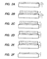
- FIGS. 2A, 2B, 2C, 2D, 2E and 2F are schematic views of another embodiment of semiconductor substrate according to the invention, showing different manufacturing steps.
- FIGS. 3A, 3B, 3C, 3D and 3E are schematic views of still another embodiment of semiconductor substrate according to the invention, showing different manufacturing steps.
- FIGS. 4A, 4B, 4C, 4D, 4E and 4F are schematic views of still another embodiments of semiconductor substrate according to the invention, showing different manufacturing steps.
- FIGS. 5A, 5B, 5C, 5CP, 5D, 5E, 5F and 5FP are schematic views of still another embodiment of semiconductor substrate according to the invention, showing different manufacturing steps.
- FIGS. 6A, 6B, 6C, 6D, 6E and 6F are schematic views of still another embodiment of semiconductor substrate according to the invention, showing different manufacturing steps.
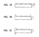
- FIGS. 7A, 7B and 7C are schematic views of still another embodiment of semiconductor substrate according to the invention, showing different manufacturing steps.
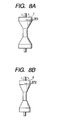
- FIGS. 8A and 8B are schematic views of edge etchers that can be used for the purpose of the present invention.
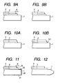
- FIGS. 9A and 9B are schematic partial cross sectional views of still another embodiment of semiconductor substrate according to the invention.
- FIGS. 10A and 10B are schematic partial cross sectional views of a semiconductor substrate prepared for the purpose of comparison.
- FIGS. 11 and 12 are schematic partial cross sectional views of still other embodiments of semiconductor substrate according to the invention.
- FIGS. 13A, 13B, 13C, 13D and 13E are schematic cross sectional views of a semiconductor substrate, showing different steps of a known method of manufacturing a semiconductor substrate.
- FIGS. 1A and 1B are a schematic plan view and a schematic cross sectional side view of a basic embodiment of semiconductor substrate according to the invention.
- the outer peripheral extremity 3A of the semiconductor layer 3 is located inside the outer peripheral extremity 1A of the support member 1 and the outer peripheral extremity 2A of the insulation layer 2 is located between the outer peripheral extremity 3A of the semiconductor layer 3 and the outer peripheral extremity 1A of the support member 1 so that the outer peripheral portion 10 of the embodiment including the semiconductor layer 3 and the insulation layer 2 shows a stepped profile. More specifically, the bottom of the outer peripheral extremity of the semiconductor layer 3 and the top of the outer peripheral extremity of the insulation layer 2 are offset relative to each other by a horizontal distance d so that, unlike FIG. 13E, the outer peripheral extremity of the semiconductor layer 3 does not show an overhanging profile. In other words, the embodiment has a terrace with width d on the outer peripheral portion of the insulation layer 2. Therefore, the outer peripheral extremity of the semiconductor layer 3 can hardly give rise to a chipping phenomenon and debris.
- the support member 1 is preferably a substrate made from a preform of a semiconductor material such as Si, Ge, GaAs or InP.
- a semiconductor material such as Si, Ge, GaAs or InP.
- Si wafers are preferably used.
- the insulation layer is preferably made of an insulating material such as silicon oxide or silicon nitride.
- the semiconductor layer preferably comprises at least a layer of a material selected from a group of semiconductor materials including Si, Ge, SiGe, SiC, GaAs, GaAlAs, InP and GaN.
- the horizontal offset d is preferably not less than 2 microns, more preferably no less than 2 microns and not more than 1,000 microns.
- the thickness of the semiconductor layer is preferably not less than 10 nanometers and not more than 10 microns, more preferably not less than 10 nanometers and not more than 2 microns.
- the thickness of the insulation layer is preferably not less than 10 nanometers and not more than 10 microns, more preferably not less than 10 nanometers and not more than 2 microns.
- a process comprising a bonding step is preferably used for preparing an SOI substrate 5 before processing the outer peripheral portion thereof.
- Specific examples of manufacturing process that can be used for the purpose of the invention include the methods described in Japanese Patent No. 2608351 and U.S. Patent No. 5,371,037, Japanese Patent Application Laid-Open No. 7-302889 and Japanese Patent Application Laid-Open No. 5-211128 and U.S. Patent No. 5,374,564.
- both the method disclosed in Japanese Patent No. 2608351 and U.S. Patent No. 5,371,037 and the one disclosed in Japanese Patent Application Laid-Open No. 7-302889 comprise steps of preparing a first member having a porous single crystal semiconductor layer and a non-porous single crystal semiconductor layer, bonding said first member and a second member with an insulation layer interposed therebetween so as to produce a multilayer structure with said non-porous single crystal semiconductor layer located inside and removing said non-porous single crystal semiconductor layer from said multilayer structure.
- Said semiconductor layer contains silicon and either of the above methods can be used to prepare an SOI substrate containing silicon single crystal whose crystallinity is as excellent as that of a single crystal wafer.
- the method disclosed in Japanese Patent Application Laid-Open No. 5-211128 and U.S. Patent No. 5,374,564 comprises steps of forming a silicon oxide layer on the surface of a single crystal silicon wafer substrate, implanting either hydrogen gas ions or rare gas ions into the wafer from the side of the silicon oxide layer, forming a micro-bubble layer in the single crystal silicon wafer, bonding the wafer to another substrate operating as support member at the side of the silicon oxide and then separating the bonded substrates along the micro-bubble layer to produce an SOI substrate. Then, this SOI substrate may be used to prepare a semiconductor substrate as described above by referring to the first embodiment of the invention.
- the wafer When a semiconductor wafer such as an Si wafer is used as starting material of an SOI substrate prepared by means of a bonding technique, it should be noted that the wafer is beveled both at the top and at the bottom of its outer peripheral extremity. Therefore, in the SOI substrate the outer peripheral extremity of the semiconductor layer (or the insulation layer) and that of the support member may be offset to a slight extent before being subjected to an operation of processing the outer peripheral portion thereof according to the invention.
- the outer peripheral portion of the semiconductor substrate including said insulation layer and said semiconductor layer is processed to show a stepped profile as seen from FIGS. 1A and 1B.
- Techniques that can preferably be used for the processing operation include wet or dry etching using an etching mask and polishing such as chemical mechanical polishing (CMP).
- CMP chemical mechanical polishing
- Both the outer peripheral portion of the semiconductor layer and that of the insulation layer may be processed to show a tapered or sloped profile in such a way that the top surface and the lateral surface thereof intersect each other with an angle greater than the right angle as will be described in greater detail hereinafter.
- the etching process may be that of wet etching or that of dry etching.
- a mixture solution of hydrogen fluoride and nitric acid or TMAH trimethylammoniumhydroxide
- TMAH trimethylammoniumhydroxide
- chlorine, CF 4 or SF 6 may be used as etchant when a dry etching technique is used.
- a hydrofluoric acid solution or a buffered hydrofluoric acid solution may popularly be used in a wet etching process, whereas CH 3 may be used in a dry etching process.
- the etching mode may be isotropic or anisotropic.
- An isotropic etching process, an edge etcher and an edge polisher may preferably be used to process the semiconductor layer and the insulation layer to make them show a tapered profile for the purpose of the invention.
- an SOI substrate 5 is prepared as shown in FIG. 2A by means of a bonding technique.
- the SOI substrate 5 comprises a support member 1, which is a single silicon substrate, an insulation film 2 formed on the support member 1 typically by means of a dry oxidation technique, using only O 2 gas, or a wet oxidation technique, using steam, and a semiconductor (silicon) layer 3 epitaxially grown on the insulation film 2 by means of CVD (chemical vapor deposition).
- CVD chemical vapor deposition
- an etching mask of photoresist 4 is formed on the silicon layer 3 in order to remove a portion of the silicon layer 3 that is located at the outer peripheral extremity thereof on the insulation film 2 and shows a weak bonding strength (FIG.2B). Then, the silicon layer 3 is etched to remove the outer peripheral extremity thereof, using the photoresist 4 as mask (FIG. 2C). After removing the photoresist 4, photoresist 6 is applied anew for etching the insulation film 2 and subjected to a patterning operation (FIG. 2D). To realize an etching selectivity for the insulation film 2 relative to the underlying support member 1, the insulation film 2 is etched by means of wet etching, using hydrofluoric acid as etchant.
- both the photoresist 4 and the photoresist 6 may be of the ordinary positive type or of the ordinary negative type.
- a popular example of photoresist of the positive type is novolak resin that can be applied by spinning. In place of patterning the applied photoresist, a mask may be bonded to the silicon layer 3 so long as an etching mask is appropriately placed in position.
- the method of preparing an SOI substrate 5 for this embodiment is not limited to the above described one, which may be replaced by some other appropriate method.
- FIGS. 3A through 3E schematically illustrate a third embodiment of manufacturing an SOI substrate according to the invention, showing different manufacturing steps.
- an SOI substrate 5 comprising an insulation film 2 and a silicon layer 3 arranged on a support member 1 is prepared (FIG. 3A).
- Photoresist 4 is applied onto the SOI substrate 5 and subjected to a patterning operation to make it show a desired pattern (FIG. 3B).
- an extreme end portion of the silicon layer 3 and also an extreme end portion of the insulation film 2 are etched out successively (FIG. 3C).
- the portion of the silicon layer 3 and that of the insulation film 2 on the support member 1 that are not covered by the photoresist 4 are removed successively.
- a semiconductor substrate according to the invention can be produced without using a photolithography process and the etching operation may be conducted by masking the silicon substrate by means of a tape.
- the peripheral area of the silicon substrate may be etched stepwise by means of an edge etcher that is adapted to etch an object only peripherally.
- a profile as shown in FIG. 2F may be produced in the outer peripheral portion by means of an edge polisher.
- FIGS. 4A through 4F schematically illustrate a fourth embodiment of manufacturing an SOI substrate according to the invention, showing different manufacturing steps.
- an SOI substrate 5 comprising a 2 ⁇ m thick insulation film 2 and a 2 ⁇ m thick silicon layer 3 arranged on a support member 1 is prepared and then, as shown in FIG. 4B, a first photoresist 4 is applied onto the SOI substrate 5 and subjected to a patterning operation to make it show a desired pattern (FIG. 3B).
- a wafer edge exposure system adapted to expose only a peripheral portion of the wafer is used to expose a circular zone located along the outer peripheral extremity of the support member and having a width of L1 to light for removal in this embodiment.
- an extreme end portion of the silicon layer 3 and that of the insulation film 2 of the SOI substrate 5 are etched successively.
- a second photoresist 6 is applied and only a peripheral portion of the photoresist 6 having a width of L2 is exposed to light by means of the wafer edge exposure system to produce a photoresist pattern as shown in FIG. 4D.
- the outer peripheral extremity of the second photoresist 6 is located inside that of the first photoresist 4 by a distance of (L2-L1).
- L1 and L2 may preferably be about 1.8mm and 2.0mm respectively. Note that the difference between the outer peripheral extremity of the first photoresist 4 and that of the second photoresist 6 can be reduced further by using an improved precision exposure system for the patterning operation.
- a phenomenon of side etching can appear to an extent equal to the film thickness (2 ⁇ m) of the insulation film 2 when the insulation film has a tapered profile with a tapering angle of about 45°.
- the silicon layer 3 can be undercut at the bottom when the width is made smaller than the possible extent of side etching of the insulation film 2 (2 ⁇ m).
- the distance between the width of the first photoresist 4 and that of the second photoresist 6 (L2-L1) needs to be greater than the extent of the side etching of the insulation film 2. While there is no upper limit for the widths, the number of devices that can be produced from the silicon active layer is reduced when the widths are too large so that, the widths should be greater than 5 microns depending on the accuracy of the exposure system and preferably between 100 microns and 500 microns when a wafer edge exposure system is used.
- any chipping phenomenon in the silicon layer 3 and the insulation film 2 of the SOI substrate 5 can reliably be prevented from appearing.
- the angle of inclination of the lateral surface of the insulation film is made to be smaller than that of the lateral surface of the semiconductor layer.
- FIGS. 5A through 5F schematically illustrate a fifth embodiment of manufacturing an SOI substrate according to the invention, showing different manufacturing steps.
- an SOI substrate 5 comprising a silicon oxide film 2 as an insulation film with a thickness T2 of 2 ⁇ m thick and a silicon layer 3 with a thickness T3 of 2 ⁇ m arranged on a supporting silicon substrate 1 is prepared by means of a bonding technique and then, as shown in FIG. 5B, a first photoresist 6 is applied onto the SOI substrate 5 and subjected to a patterning operation to make it show a desired pattern.
- TMAH trimethylammonium-hydroxide
- etching solution a mixture of hydrofluoric acid and nitric acid
- RIE reactive ion etching
- CDE chemical dry etching
- an isotropic radical etching operation can be realized in a parallel plate reactive ion etching system using SF 6 gas and O 2 gas with a high electric discharge pressure of 50Pa and adapted to reduce the mean free path of ions and hence the rate of ionic etching.
- the etching operation proceeds perfectly isotropically so that the lateral surface of the silicon layer 3 is tapered with an obtuse angle between the lateral surface and the top surface, while angle AG3 is substantially equal to 45° (FIG. 5CP).
- angle AG3 is substantially equal to 45° (FIG. 5CP).
- a sufficiently large etch selectivity can be secured between the rate of etching the underlying silicon oxide film 2 and that of etching the silicon layer 3 so that consequently only the silicon layer 3 is so etched as to show a tapered profile.
- a second photoresist 4 is applied to the wafer and only the zone along the wafer edge with the width of L1 is exposed to light by using a photomask having a contour similar to that of the first photomask but greater than the latter by 8 microns to produce a patterned photoresist 4 as shown in FIG. 5D. If L1 is 1.992mm, the resist pattern of the photoresist 2 has the outer peripheral extremity aligned with a line drawn outside the first photoresist 6 and separated from the latter by 8 microns.
- etching solution such as a buffered hydrofluoric acid (BHF) solution will suitably be used for the etching operation.
- BHF buffered hydrofluoric acid
- RIE reactive ion etching
- CDE chemical dry etching
- an isotropic etching operation can be realized by wet etching using a buffered hydrofluoric acid (BHF) solution until the silicon oxide film 2 is over-etched to a slight extent and angle AG2 becomes substantially equal to 30 ⁇ .
- BHF buffered hydrofluoric acid
- a sufficiently large etch selectivity can be secured between the rate of etching the underlying silicon oxide film 2 and that of etching the silicon layer 3 so that consequently only the silicon oxide film 2 is so etched as to show a tapered profile with angle AG2 of 30 as shown in FIG 5E (see also FIG 5FP).
- the silicon oxide film 2 When the silicon oxide film 2 is etched to make it show a tapered profile in the outer peripheral portion with angle AG2 equal to 30°, a side etching of 2.8 ⁇ m occurs to the insulating silicon oxide film 2 having a film thickness of 2 ⁇ m.
- the silicon layer 3 can be undercut at the bottom when the width is made smaller than the possible extent of side etching of the insulation film 2.
- the difference (L2-L1) between the width of the first photoresist 6 and that of the second photoresist 4 needs to be greater than the extent of the side etching of the insulation film 2. While there is no upper limit for the widths, the number of devices that can be produced from the silicon active layer is reduced when the widths are too large so that, they should be greater than 5 microns depending on the accuracy of the exposure system and preferably between 100 microns and 500 microns when a wafer edge exposure system is used.
- the photoresist 4 is removed to produce a tapered and terraced profile as shown in FIG. 5F with the angle AG2 of 30° and a terrace width d of 5.2 ⁇ m.
- FIGS. 6A through 6F schematically illustrate a sixth embodiment of manufacturing an SOI substrate according to the invention, showing different manufacturing steps.
- an 8-inch (diameter, 200mm) SOI substrate 5 comprising a 200nm thick silicon oxide film 2 as an insulation film and a 200nm thick silicon layer 3 arranged on a supporting silicon substrate 1 is prepared by means of a bonding technique.
- a first mask tape 14 is applied onto the SOI substrate 5 with the center of the mask tape aligned with that of the wafer.
- a mask tape 14 with a diameter of e.g. 196.8mm may suitably be used for this embodiment.
- FIG. 6C the extreme end portion of the silicon layer 3 and that of the insulation film 2 are etched out successively.
- the lateral side of the insulation film 2 and that of the silicon layer 3 are made to show an acute angle of inclination by controlling the duration of the etching operation.
- the first mask tape 14 is arranged inside the second mask tape 16 and offset by 0.4mm at any point on its outer boundary.
- This value is selected in view of the alignment accuracy of the tape applicator machine expected to be used. For this embodiment, it is about ⁇ 0.2mm. If a tape applicator machine with a better alignment accuracy is used, the difference (L2-L1) between the width of the zone exposed from the first mask tape 14 and that of the zone exposed from the second mask tape 16 can be further reduced.
- the widths (L1, L2) While there is no upper limit for the widths (L1, L2), the number of devices that can be produced from the silicon active layer is reduced when they are too large so that, they should be between 10 microns and 1 millimeter depending on the accuracy of the tape applicator machine and preferably between 100 microns and 500 microns in practical uses.
- the cost of the mask tapes is as low as about a half of the cost of using photoresist, including the cost of the developing solution, and hence the technique of using mask tapes provides remarkable practical advantages over the etching technique particularly in view of the fact that the tape applicator machine and the tape peeling machine are less costly than a resist coater and an exposure system.
- FIGS. 7A through 7C schematically illustrate a seventh embodiment of manufacturing an SOI substrate according to the invention, showing different manufacturing steps.
- an 8-inch (diameter, 200mm) SOI substrate 5 comprising a 200nm thick silicon oxide film 2 as an insulation layer and a 200nm thick silicon layer 3 arranged on a supporting silicon substrate 1 is prepared by means of a bonding technique.
- the silicon layer 3 of the SOI substrate 5 is etched by means of a rotary-type sheet edge etcher adapted to etch wafers on a sheet by sheet basis and having a configuration as shown in FIG. 8A.
- a rotary-type sheet edge etcher adapted to etch wafers on a sheet by sheet basis and having a configuration as shown in FIG. 8A.
- Such an edge etcher is described in Japanese Patent Publication No. 7-15897 and comprises a roller pad 7 so that the wafer is etched as the roller pad 7 soaked with etching solution is pressed against it.
- nitrogen gas (N 2 ) blows out through a ring-shaped nozzle (not shown) arranged above the substrate in order to prevent the steam of the etching solution from flowing onto the surface of the wafer so that the edge etcher does not require the use of an etching mask.
- the depth DP3 of the roller pad 7 for etching the silicon layer 3 will be about 1.8mm and the etching depth can be controlled by appropriately selecting the pressure under which the roller pad 7 is pressed against the wafer. Then, the silicon layer 3 will be etched to show a profile mildly tapered from the wafer end by about 1.8 to 2.0mm. At the same time, a sufficiently large etch selectivity can be secured between the rate of etching the silicon layer and that of etching the silicon oxide film 2 by using an alkaline TMAH (trimethylammoniumhydroxide) etching solution so that consequently only the silicon layer 3 is etched. A desired etch selectivity can also be selected by using an appropriate composition ratio of hydrofluoric acid and nitric acid. Thus, the silicon layer is processed to show a profile as illustrated in FIG. 7B.
- TMAH trimethylammoniumhydroxide
- the outer peripheral portion of the silicon oxide film 2 is etched by means of an apparatus as shown in FIG. 8B.
- the roller pad 8 to be used for etching the silicon oxide film 2 has a depth DP2 of about 1.4mm and the etching depth can be controlled by appropriately selecting the pressure under which the roller pad 8 is pressed against the wafer.
- the edge etcher to be used for this embodiment comprises roller pads for the first and second etching operations having respective depths DP3 and DP2 of 1.4mm and 1.8mm, the difference being 0.4mm.
- This difference or the width of the exposed zone (f-e) can be reduced by selecting appropriate parameters because the tapered profile obtained by the etching operations can be modified as a function of the types and compositions of the etching solutions, the pressures under which the roller pads are pressed against the wafer and other factors.
- the width (f-e) While there is no upper limit for the width (f-e), the number of devices that can be produced from the silicon active layer is reduced when the width (f-e) is too large so that the width (f-e) should be between 10 microns and lmm when an ordinary edge etcher is used and preferably it may be between 100 microns and 500 microns when the etching conditions are optimized. Finally, the etching solution is replaced by pure water to produce an outer peripheral portion having a mildly tapered and stepped profile.
- the width of the removed portion can be considerably large due to the mildly tapered profile, the use of an edge etcher is advantageous in terms of cost because it does not use photoresist nor tapes.
- An edge polisher that can be used for the purpose of the invention is of the rotary-type having a rotating pad adapted to be supplied with a polishing agent and effectively polish the substrate if the angle between the pad and the substrate is varied.
- the profile of the polished product can be controlled by controlling the pressure under which the pad is pressed against the substrate and selecting the material and the hardness of the pad.
- the polishing operation can be time consuming if the SOI layer has a large thickness and the outer peripheral portion of the SOI substrate can be removed by a large width to produce a mildly tapered profile
- the use of an edge polisher is advantageous in terms of cost because it does not use photoresist nor tapes either.
- the use of a tape and that of an edge etcher may be combined so that a tape is used for the first (or second) etching operation whereas an edge etcher (or an edge polisher) is used for the second (or first, whichever appropriate) etching operation.
- the use of photoresist, that of tapes, that of an edge etcher and that of an edge polisher may appropriately be combined for the purpose of the present invention from the viewpoint of the width of the zone to be removed from the SOI substrate, the tapered profile and the processing cost.
- FIG. 9A is a schematic illustration of an outer peripheral portion of an eighth embodiment of semiconductor substrate according to the invention and FIG. 9B is a schematic illustration of the outer peripheral portion (S12) of the same embodiment as seen after having been etched at the lateral side thereof.
- FIG. 10A is a schematic illustration of an outer peripheral portion of a semiconductor substrate prepared for the purpose of comparison and FIG. 10B is a schematic illustration of the outer peripheral portion of the same semiconductor substrate as seen after having been etched at the lateral side thereof.
- an undercut UC is produced under the outer peripheral extremity of the semiconductor layer 3 (at the top of the outer peripheral extremity of the insulation layer 2) as shown in FIG. 10B.
- this limit may be defined as a function of the extent of side etching particularly when the extent of side etching is remarkable in the process that involves a side etching effect exerted on the insulation layer 2.
- the lower limit of the offset d is defined as a function of the extent of side etching
- the upper limit of the offset d may be defined as a function of the extent to which the semiconductor layer is effectively utilized and depending on the wafer size, the required size and number of the semiconductor chip as well as other factors.
- the offset d is typically not less than 2 microns and not more than 1 millimeter, preferably not less than 5 microns and not less than 1 millimeter, more preferably not less than 100 microns and not more than 500 microns.
- FIG. 11 is a schematic illustration of an extreme portion of a ninth embodiment of semiconductor substrate according to the invention. This embodiment is obtained by modifying the structure of FIG. 9A and thin insulation films 24, 21, 22 and 23 are formed respectively on the lateral surface of the semiconductor layer 3 and the bottom surface, the lateral surface and the top surface of the peripheral portion of the support member 1.
- the bottom of the outer peripheral portion of the semiconductor layer 3 and the top of the outer peripheral portion of the insulation layer 2 are offset by d, which is not smaller than 2 microns to show a stepped profile along the outer peripheral extremity of the semiconductor substrate so that any undercut can hardly be produced there more than ever.
- Such a structure can be obtained either by oxidizing the structure of FIG. 9A with masking the top surface of the semiconductor layer 3, or by oxidizing the entire surface of the structure of FIG. 9A and subsequently removing the oxide film from the top surface of the semiconductor layer 3.
- FIG. 12 is a schematic cross sectional view of a tenth embodiment of semiconductor substrate according to the invention, showing only an outer peripheral portion thereof.
- the outer peripheral extremity of the support member 1 is beveled both at the top and at the bottom.
- the bottom of the outer peripheral extremity of the semiconductor layer 3 and the top of the outer peripheral extremity of the insulation layer 2 are offset by more than 2 ⁇ m to produce a terrace on the top surface of the insulation layer 2.
- the bottom of the outer peripheral extremity of the insulation layer 2 and the outer peripheral extremity of the support member 1 are offset by more than 1mm.
- the semiconductor layer 3 has a thickness greater than that of the insulation layer 2 in the structure of FIG. 12, the thickness of the former may alternatively be made smaller than that of the latter. Additionally, the lateral surfaces of the layers 2 and 3 may be tapered and/or the lateral surface of the outer peripheral portion of and the bottom surface of the support member may be coated with insulation films (21, 22) as in FIG. 11. Note that the support member 1 of a semiconductor substrate according to the invention has a thickness of several hundred microns, which is significantly greater than those of the layers 2 and 3.
- both the semiconductor layer and the insulation layer may be removed partly at an area having a weak bonding strength, particularly in a outer peripheral extremity portion of the SOI substrate to produce a stepped profile along the outer peripheral extremities of the semiconductor layer and the insulation layer, that can effectively prevent any chipping phenomenon from appearing so that high quality SOI substrates may be manufactured on a stable basis.
- the lateral surface of the semiconductor layer and that of the insulation layer may be inclined to prevent the appearance of a chipping phenomenon and the production of debris so that high quality semiconductor devices may be manufactured at a high yield.
- an SIMOX wafer can be used as SOI substrate for the purpose of the invention.
- An 8-inch Si wafer was prepared as prime wafer and the surface was made porous by anodization to a depth of about 10 ⁇ m from the surface.
- the produced porous layer was thermally oxidized at 400 °C and then dipped into a dilute hydrofluoric acid solution to remove the oxide film from the top surface of the porous layer. Subsequently, the specimen was prebaked in a hydrogen atmosphere and then a non-porous Si layer was made to epitaxially grow to a height of 120nm on the porous layer by CVD.
- the surface of the Si layer obtained by epitaxial growth was then oxidized to produce an about 40nm thick oxide film and a separately prepared 8-inch wafer was bonded as handle wafer to the prime wafer, before the assembly was subjected to a heat treatment process.
- the prime wafer was ground from the rear surface to expose the porous layer by means of RIE and then the porous layer was selectively removed by means of an etching solution containing hydrofluoric acid, hydrogen peroxide and alcohol. Then, the specimen was heat treated in a hydrogen atmosphere and the exposed surface of the non-porous Si layer that had been transferred onto the handle wafer was smoothed to produce an SOI substrate.
- the number of particles with a diameter greater than 0.15 ⁇ m was between 0.02/cm 2 and 0.1/cm 2 and did not vary remarkably for all the specimens.
- a number of SOI substrates were prepared as in the above example. Subsequently, they were subjected to the processing steps as described above by referring to FIGS. 13A through 13E. Then, the obtained semiconductor substrates were cleansed repeatedly and the number of particles adhering to each of the specimens was observed as in the case of the above example..
- the number of particles with a diameter greater than 0.15 ⁇ m was between 0.05/cm 2 and 4/cm 2 and remarkably varied after each measurement.
- Each increase in the number of particles was dominated by particles with a diameter between 0.05 ⁇ m and 0.4 ⁇ m.
Landscapes
- Element Separation (AREA)
- Weting (AREA)
- Drying Of Semiconductors (AREA)
- Mechanical Treatment Of Semiconductor (AREA)
- Diaphragms For Electromechanical Transducers (AREA)
- Photovoltaic Devices (AREA)
- Thin Film Transistor (AREA)
Applications Claiming Priority (4)
| Application Number | Priority Date | Filing Date | Title |
|---|---|---|---|
| JP2306698 | 1998-02-04 | ||
| JP2306698 | 1998-02-04 | ||
| JP37031698 | 1998-12-25 | ||
| JP37031698 | 1998-12-25 |
Publications (2)
| Publication Number | Publication Date |
|---|---|
| EP0935280A1 true EP0935280A1 (de) | 1999-08-11 |
| EP0935280B1 EP0935280B1 (de) | 2004-06-09 |
Family
ID=26360364
Family Applications (1)
| Application Number | Title | Priority Date | Filing Date |
|---|---|---|---|
| EP99300620A Expired - Lifetime EP0935280B1 (de) | 1998-02-04 | 1999-01-28 | SOI Substrat |
Country Status (8)
| Country | Link |
|---|---|
| US (3) | US6417108B1 (de) |
| EP (1) | EP0935280B1 (de) |
| KR (1) | KR100360979B1 (de) |
| CN (1) | CN1145200C (de) |
| AT (1) | ATE268943T1 (de) |
| DE (1) | DE69917819T2 (de) |
| SG (1) | SG78332A1 (de) |
| TW (1) | TW454244B (de) |
Cited By (7)
| Publication number | Priority date | Publication date | Assignee | Title |
|---|---|---|---|---|
| WO2003098695A1 (en) * | 2002-05-20 | 2003-11-27 | Sumitomo Mitsubishi Silicon Corporation | Laminated substrate, method of manufacturing the substrate, and wafer outer periphery pressing jigs used for the method |
| FR2880184A1 (fr) * | 2004-12-28 | 2006-06-30 | Commissariat Energie Atomique | Procede de detourage d'une structure obtenue par assemblage de deux plaques |
| EP1170801B1 (de) * | 1999-10-14 | 2006-07-26 | Shin-Etsu Handotai Company Limited | Verbundscheiben-herstellungsmethode |
| EP2402983A4 (de) * | 2009-02-26 | 2012-07-25 | Shinetsu Handotai Kk | Verfahren zur herstellung eines soi-wafers |
| US8298916B2 (en) | 2010-03-02 | 2012-10-30 | Soitec | Process for fabricating a multilayer structure with post-grinding trimming |
| US8530331B2 (en) | 2006-04-10 | 2013-09-10 | Commissariat A L'energie Atomique | Process for assembling substrates with low-temperature heat treatments |
| CN106803482A (zh) * | 2017-02-14 | 2017-06-06 | 上海华虹宏力半导体制造有限公司 | 一种用于减少晶圆边缘良率测试问题的方法 |
Families Citing this family (276)
| Publication number | Priority date | Publication date | Assignee | Title |
|---|---|---|---|---|
| US20020166284A1 (en) * | 2001-03-12 | 2002-11-14 | Weder Donald E. | Sheets of material having a first printed pattern on an upper surface thereof and a second printed pattern on a lower surface thereof |
| IL119523A0 (en) * | 1996-10-30 | 1997-01-10 | Algotec Systems Ltd | Data distribution system |
| US8018058B2 (en) * | 2004-06-21 | 2011-09-13 | Besang Inc. | Semiconductor memory device |
| US8058142B2 (en) * | 1996-11-04 | 2011-11-15 | Besang Inc. | Bonded semiconductor structure and method of making the same |
| US20050280155A1 (en) * | 2004-06-21 | 2005-12-22 | Sang-Yun Lee | Semiconductor bonding and layer transfer method |
| JP3687848B2 (ja) * | 2001-11-28 | 2005-08-24 | 日立金属株式会社 | 光合分波器用薄膜フィルターおよびその製造方法 |
| KR20030044205A (ko) * | 2001-11-29 | 2003-06-09 | 동부전자 주식회사 | 반도체 제조 장치 및 방법 |
| US6768965B2 (en) * | 2002-04-18 | 2004-07-27 | Seh America, Inc. | Methods and computer program products for characterizing a crystalline structure |
| FR2842651B1 (fr) * | 2002-07-17 | 2005-07-08 | Procede de lissage du contour d'une couche utile de materiau reportee sur un substrat support | |
| US7594967B2 (en) * | 2002-08-30 | 2009-09-29 | Amberwave Systems Corporation | Reduction of dislocation pile-up formation during relaxed lattice-mismatched epitaxy |
| KR100951898B1 (ko) * | 2002-12-09 | 2010-04-09 | 삼성전자주식회사 | 포토레지스트 제거용 스트리핑 조성물 및 이를 사용한액정 표시 장치의 박막 트랜지스터 기판의 제조방법 |
| US20100133695A1 (en) * | 2003-01-12 | 2010-06-03 | Sang-Yun Lee | Electronic circuit with embedded memory |
| FR2850390B1 (fr) * | 2003-01-24 | 2006-07-14 | Soitec Silicon On Insulator | Procede d'elimination d'une zone peripherique de colle lors de la fabrication d'un substrat composite |
| FR2852445B1 (fr) * | 2003-03-14 | 2005-05-20 | Soitec Silicon On Insulator | Procede de realisation de substrats ou composants sur substrats avec transfert de couche utile, pour la microelectronique, l'optoelectronique ou l'optique |
| US7122095B2 (en) * | 2003-03-14 | 2006-10-17 | S.O.I.Tec Silicon On Insulator Technologies S.A. | Methods for forming an assembly for transfer of a useful layer |
| US7022247B2 (en) * | 2003-03-26 | 2006-04-04 | Union Semiconductor Technology Corporation | Process to form fine features using photolithography and plasma etching |
| US8071438B2 (en) * | 2003-06-24 | 2011-12-06 | Besang Inc. | Semiconductor circuit |
| US20100190334A1 (en) * | 2003-06-24 | 2010-07-29 | Sang-Yun Lee | Three-dimensional semiconductor structure and method of manufacturing the same |
| US7105431B2 (en) * | 2003-08-22 | 2006-09-12 | Micron Technology, Inc. | Masking methods |
| US20050045206A1 (en) * | 2003-08-26 | 2005-03-03 | Smith Patricia Beauregard | Post-etch clean process for porous low dielectric constant materials |
| US7354631B2 (en) * | 2003-11-06 | 2008-04-08 | Micron Technology, Inc. | Chemical vapor deposition apparatus and methods |
| US20050161808A1 (en) * | 2004-01-22 | 2005-07-28 | Anderson Douglas G. | Wafer, intermediate wafer assembly and associated method for fabricating a silicon on insulator wafer having an improved edge profile |
| US7115524B2 (en) * | 2004-05-17 | 2006-10-03 | Micron Technology, Inc. | Methods of processing a semiconductor substrate |
| US7364953B2 (en) * | 2004-10-22 | 2008-04-29 | Freescale Semiconductor, Inc. | Manufacturing method to construct semiconductor-on-insulator with conductor layer sandwiched between buried dielectric layer and semiconductor layers |
| DE102004054564B4 (de) * | 2004-11-11 | 2008-11-27 | Siltronic Ag | Halbleitersubstrat und Verfahren zu dessen Herstellung |
| CN100437353C (zh) * | 2004-12-29 | 2008-11-26 | 南京大学 | 纳米印章技术中纳米级模板的制备方法 |
| US8367524B2 (en) * | 2005-03-29 | 2013-02-05 | Sang-Yun Lee | Three-dimensional integrated circuit structure |
| US20110143506A1 (en) * | 2009-12-10 | 2011-06-16 | Sang-Yun Lee | Method for fabricating a semiconductor memory device |
| KR100855834B1 (ko) * | 2007-05-25 | 2008-09-01 | 주식회사 하이닉스반도체 | 반도체 소자 및 그 제조 방법 |
| JP5245380B2 (ja) * | 2007-06-21 | 2013-07-24 | 信越半導体株式会社 | Soiウェーハの製造方法 |
| FR2935535B1 (fr) * | 2008-09-02 | 2010-12-10 | S O I Tec Silicon On Insulator Tech | Procede de detourage mixte. |
| FR2935536B1 (fr) * | 2008-09-02 | 2010-09-24 | Soitec Silicon On Insulator | Procede de detourage progressif |
| US8476165B2 (en) | 2009-04-01 | 2013-07-02 | Tokyo Electron Limited | Method for thinning a bonding wafer |
| US9711407B2 (en) | 2009-04-14 | 2017-07-18 | Monolithic 3D Inc. | Method of manufacturing a three dimensional integrated circuit by transfer of a mono-crystalline layer |
| US9577642B2 (en) | 2009-04-14 | 2017-02-21 | Monolithic 3D Inc. | Method to form a 3D semiconductor device |
| US8378715B2 (en) | 2009-04-14 | 2013-02-19 | Monolithic 3D Inc. | Method to construct systems |
| US8373439B2 (en) | 2009-04-14 | 2013-02-12 | Monolithic 3D Inc. | 3D semiconductor device |
| US9509313B2 (en) | 2009-04-14 | 2016-11-29 | Monolithic 3D Inc. | 3D semiconductor device |
| US8362482B2 (en) | 2009-04-14 | 2013-01-29 | Monolithic 3D Inc. | Semiconductor device and structure |
| US7986042B2 (en) | 2009-04-14 | 2011-07-26 | Monolithic 3D Inc. | Method for fabrication of a semiconductor device and structure |
| US8405420B2 (en) | 2009-04-14 | 2013-03-26 | Monolithic 3D Inc. | System comprising a semiconductor device and structure |
| US8058137B1 (en) | 2009-04-14 | 2011-11-15 | Monolithic 3D Inc. | Method for fabrication of a semiconductor device and structure |
| US8362800B2 (en) | 2010-10-13 | 2013-01-29 | Monolithic 3D Inc. | 3D semiconductor device including field repairable logics |
| US8384426B2 (en) | 2009-04-14 | 2013-02-26 | Monolithic 3D Inc. | Semiconductor device and structure |
| US8427200B2 (en) | 2009-04-14 | 2013-04-23 | Monolithic 3D Inc. | 3D semiconductor device |
| US8669778B1 (en) | 2009-04-14 | 2014-03-11 | Monolithic 3D Inc. | Method for design and manufacturing of a 3D semiconductor device |
| US8754533B2 (en) | 2009-04-14 | 2014-06-17 | Monolithic 3D Inc. | Monolithic three-dimensional semiconductor device and structure |
| US8395191B2 (en) | 2009-10-12 | 2013-03-12 | Monolithic 3D Inc. | Semiconductor device and structure |
| US11374118B2 (en) | 2009-10-12 | 2022-06-28 | Monolithic 3D Inc. | Method to form a 3D integrated circuit |
| US10354995B2 (en) | 2009-10-12 | 2019-07-16 | Monolithic 3D Inc. | Semiconductor memory device and structure |
| US8294159B2 (en) | 2009-10-12 | 2012-10-23 | Monolithic 3D Inc. | Method for fabrication of a semiconductor device and structure |
| US8536023B2 (en) | 2010-11-22 | 2013-09-17 | Monolithic 3D Inc. | Method of manufacturing a semiconductor device and structure |
| US11018133B2 (en) | 2009-10-12 | 2021-05-25 | Monolithic 3D Inc. | 3D integrated circuit |
| US8742476B1 (en) | 2012-11-27 | 2014-06-03 | Monolithic 3D Inc. | Semiconductor device and structure |
| US10388863B2 (en) | 2009-10-12 | 2019-08-20 | Monolithic 3D Inc. | 3D memory device and structure |
| US10366970B2 (en) | 2009-10-12 | 2019-07-30 | Monolithic 3D Inc. | 3D semiconductor device and structure |
| US11984445B2 (en) | 2009-10-12 | 2024-05-14 | Monolithic 3D Inc. | 3D semiconductor devices and structures with metal layers |
| US12027518B1 (en) | 2009-10-12 | 2024-07-02 | Monolithic 3D Inc. | 3D semiconductor devices and structures with metal layers |
| US9099424B1 (en) | 2012-08-10 | 2015-08-04 | Monolithic 3D Inc. | Semiconductor system, device and structure with heat removal |
| US10043781B2 (en) | 2009-10-12 | 2018-08-07 | Monolithic 3D Inc. | 3D semiconductor device and structure |
| US10910364B2 (en) | 2009-10-12 | 2021-02-02 | Monolitaic 3D Inc. | 3D semiconductor device |
| US8476145B2 (en) | 2010-10-13 | 2013-07-02 | Monolithic 3D Inc. | Method of fabricating a semiconductor device and structure |
| US8450804B2 (en) | 2011-03-06 | 2013-05-28 | Monolithic 3D Inc. | Semiconductor device and structure for heat removal |
| US10157909B2 (en) | 2009-10-12 | 2018-12-18 | Monolithic 3D Inc. | 3D semiconductor device and structure |
| US8581349B1 (en) | 2011-05-02 | 2013-11-12 | Monolithic 3D Inc. | 3D memory semiconductor device and structure |
| KR101224140B1 (ko) * | 2009-12-30 | 2013-01-18 | 에스케이하이닉스 주식회사 | 반도체 장치 제조방법 |
| US8373230B1 (en) | 2010-10-13 | 2013-02-12 | Monolithic 3D Inc. | Method for fabrication of a semiconductor device and structure |
| US8541819B1 (en) | 2010-12-09 | 2013-09-24 | Monolithic 3D Inc. | Semiconductor device and structure |
| US8461035B1 (en) | 2010-09-30 | 2013-06-11 | Monolithic 3D Inc. | Method for fabrication of a semiconductor device and structure |
| US8026521B1 (en) | 2010-10-11 | 2011-09-27 | Monolithic 3D Inc. | Semiconductor device and structure |
| US9099526B2 (en) | 2010-02-16 | 2015-08-04 | Monolithic 3D Inc. | Integrated circuit device and structure |
| US8492886B2 (en) | 2010-02-16 | 2013-07-23 | Monolithic 3D Inc | 3D integrated circuit with logic |
| FR2961630B1 (fr) | 2010-06-22 | 2013-03-29 | Soitec Silicon On Insulator Technologies | Appareil de fabrication de dispositifs semi-conducteurs |
| KR101134819B1 (ko) | 2010-07-02 | 2012-04-13 | 이상윤 | 반도체 메모리 장치의 제조 방법 |
| US9219005B2 (en) | 2011-06-28 | 2015-12-22 | Monolithic 3D Inc. | Semiconductor system and device |
| US9953925B2 (en) | 2011-06-28 | 2018-04-24 | Monolithic 3D Inc. | Semiconductor system and device |
| US8642416B2 (en) | 2010-07-30 | 2014-02-04 | Monolithic 3D Inc. | Method of forming three dimensional integrated circuit devices using layer transfer technique |
| US10217667B2 (en) | 2011-06-28 | 2019-02-26 | Monolithic 3D Inc. | 3D semiconductor device, fabrication method and system |
| US8901613B2 (en) | 2011-03-06 | 2014-12-02 | Monolithic 3D Inc. | Semiconductor device and structure for heat removal |
| US8338266B2 (en) | 2010-08-11 | 2012-12-25 | Soitec | Method for molecular adhesion bonding at low pressure |
| FR2964193A1 (fr) | 2010-08-24 | 2012-03-02 | Soitec Silicon On Insulator | Procede de mesure d'une energie d'adhesion, et substrats associes |
| US8963337B2 (en) * | 2010-09-29 | 2015-02-24 | Varian Semiconductor Equipment Associates | Thin wafer support assembly |
| US10497713B2 (en) | 2010-11-18 | 2019-12-03 | Monolithic 3D Inc. | 3D semiconductor memory device and structure |
| US11482440B2 (en) | 2010-12-16 | 2022-10-25 | Monolithic 3D Inc. | 3D semiconductor device and structure with a built-in test circuit for repairing faulty circuits |
| US8163581B1 (en) | 2010-10-13 | 2012-04-24 | Monolith IC 3D | Semiconductor and optoelectronic devices |
| US12362219B2 (en) | 2010-11-18 | 2025-07-15 | Monolithic 3D Inc. | 3D semiconductor memory device and structure |
| US8273610B2 (en) | 2010-11-18 | 2012-09-25 | Monolithic 3D Inc. | Method of constructing a semiconductor device and structure |
| US10896931B1 (en) | 2010-10-11 | 2021-01-19 | Monolithic 3D Inc. | 3D semiconductor device and structure |
| US11315980B1 (en) | 2010-10-11 | 2022-04-26 | Monolithic 3D Inc. | 3D semiconductor device and structure with transistors |
| US11158674B2 (en) | 2010-10-11 | 2021-10-26 | Monolithic 3D Inc. | Method to produce a 3D semiconductor device and structure |
| US11024673B1 (en) | 2010-10-11 | 2021-06-01 | Monolithic 3D Inc. | 3D semiconductor device and structure |
| US11227897B2 (en) | 2010-10-11 | 2022-01-18 | Monolithic 3D Inc. | Method for producing a 3D semiconductor memory device and structure |
| US11600667B1 (en) | 2010-10-11 | 2023-03-07 | Monolithic 3D Inc. | Method to produce 3D semiconductor devices and structures with memory |
| US11469271B2 (en) | 2010-10-11 | 2022-10-11 | Monolithic 3D Inc. | Method to produce 3D semiconductor devices and structures with memory |
| US11257867B1 (en) | 2010-10-11 | 2022-02-22 | Monolithic 3D Inc. | 3D semiconductor device and structure with oxide bonds |
| US8114757B1 (en) | 2010-10-11 | 2012-02-14 | Monolithic 3D Inc. | Semiconductor device and structure |
| US10290682B2 (en) | 2010-10-11 | 2019-05-14 | Monolithic 3D Inc. | 3D IC semiconductor device and structure with stacked memory |
| US11018191B1 (en) | 2010-10-11 | 2021-05-25 | Monolithic 3D Inc. | 3D semiconductor device and structure |
| US11437368B2 (en) | 2010-10-13 | 2022-09-06 | Monolithic 3D Inc. | Multilevel semiconductor device and structure with oxide bonding |
| US11605663B2 (en) | 2010-10-13 | 2023-03-14 | Monolithic 3D Inc. | Multilevel semiconductor device and structure with image sensors and wafer bonding |
| US11164898B2 (en) | 2010-10-13 | 2021-11-02 | Monolithic 3D Inc. | Multilevel semiconductor device and structure |
| US10998374B1 (en) | 2010-10-13 | 2021-05-04 | Monolithic 3D Inc. | Multilevel semiconductor device and structure |
| US11984438B2 (en) | 2010-10-13 | 2024-05-14 | Monolithic 3D Inc. | Multilevel semiconductor device and structure with oxide bonding |
| US11869915B2 (en) | 2010-10-13 | 2024-01-09 | Monolithic 3D Inc. | Multilevel semiconductor device and structure with image sensors and wafer bonding |
| US11929372B2 (en) | 2010-10-13 | 2024-03-12 | Monolithic 3D Inc. | Multilevel semiconductor device and structure with image sensors and wafer bonding |
| US10978501B1 (en) | 2010-10-13 | 2021-04-13 | Monolithic 3D Inc. | Multilevel semiconductor device and structure with waveguides |
| US11855114B2 (en) | 2010-10-13 | 2023-12-26 | Monolithic 3D Inc. | Multilevel semiconductor device and structure with image sensors and wafer bonding |
| US11855100B2 (en) | 2010-10-13 | 2023-12-26 | Monolithic 3D Inc. | Multilevel semiconductor device and structure with oxide bonding |
| US9197804B1 (en) | 2011-10-14 | 2015-11-24 | Monolithic 3D Inc. | Semiconductor and optoelectronic devices |
| US11163112B2 (en) | 2010-10-13 | 2021-11-02 | Monolithic 3D Inc. | Multilevel semiconductor device and structure with electromagnetic modulators |
| US11694922B2 (en) | 2010-10-13 | 2023-07-04 | Monolithic 3D Inc. | Multilevel semiconductor device and structure with oxide bonding |
| US11327227B2 (en) | 2010-10-13 | 2022-05-10 | Monolithic 3D Inc. | Multilevel semiconductor device and structure with electromagnetic modulators |
| US12360310B2 (en) | 2010-10-13 | 2025-07-15 | Monolithic 3D Inc. | Multilevel semiconductor device and structure with oxide bonding |
| US11133344B2 (en) | 2010-10-13 | 2021-09-28 | Monolithic 3D Inc. | Multilevel semiconductor device and structure with image sensors |
| US11063071B1 (en) | 2010-10-13 | 2021-07-13 | Monolithic 3D Inc. | Multilevel semiconductor device and structure with waveguides |
| US10833108B2 (en) | 2010-10-13 | 2020-11-10 | Monolithic 3D Inc. | 3D microdisplay device and structure |
| US12094892B2 (en) | 2010-10-13 | 2024-09-17 | Monolithic 3D Inc. | 3D micro display device and structure |
| US11404466B2 (en) | 2010-10-13 | 2022-08-02 | Monolithic 3D Inc. | Multilevel semiconductor device and structure with image sensors |
| US10943934B2 (en) | 2010-10-13 | 2021-03-09 | Monolithic 3D Inc. | Multilevel semiconductor device and structure |
| US8379458B1 (en) | 2010-10-13 | 2013-02-19 | Monolithic 3D Inc. | Semiconductor device and structure |
| US11043523B1 (en) | 2010-10-13 | 2021-06-22 | Monolithic 3D Inc. | Multilevel semiconductor device and structure with image sensors |
| US10679977B2 (en) | 2010-10-13 | 2020-06-09 | Monolithic 3D Inc. | 3D microdisplay device and structure |
| US12080743B2 (en) | 2010-10-13 | 2024-09-03 | Monolithic 3D Inc. | Multilevel semiconductor device and structure with image sensors and wafer bonding |
| US11804396B2 (en) | 2010-11-18 | 2023-10-31 | Monolithic 3D Inc. | Methods for producing a 3D semiconductor device and structure with memory cells and multiple metal layers |
| US11569117B2 (en) | 2010-11-18 | 2023-01-31 | Monolithic 3D Inc. | 3D semiconductor device and structure with single-crystal layers |
| US12136562B2 (en) | 2010-11-18 | 2024-11-05 | Monolithic 3D Inc. | 3D semiconductor device and structure with single-crystal layers |
| US11355381B2 (en) | 2010-11-18 | 2022-06-07 | Monolithic 3D Inc. | 3D semiconductor memory device and structure |
| US11443971B2 (en) | 2010-11-18 | 2022-09-13 | Monolithic 3D Inc. | 3D semiconductor device and structure with memory |
| US11923230B1 (en) | 2010-11-18 | 2024-03-05 | Monolithic 3D Inc. | 3D semiconductor device and structure with bonding |
| US11854857B1 (en) | 2010-11-18 | 2023-12-26 | Monolithic 3D Inc. | Methods for producing a 3D semiconductor device and structure with memory cells and multiple metal layers |
| US12154817B1 (en) | 2010-11-18 | 2024-11-26 | Monolithic 3D Inc. | Methods for producing a 3D semiconductor memory device and structure |
| US12068187B2 (en) | 2010-11-18 | 2024-08-20 | Monolithic 3D Inc. | 3D semiconductor device and structure with bonding and DRAM memory cells |
| US11107721B2 (en) | 2010-11-18 | 2021-08-31 | Monolithic 3D Inc. | 3D semiconductor device and structure with NAND logic |
| US12243765B2 (en) | 2010-11-18 | 2025-03-04 | Monolithic 3D Inc. | 3D semiconductor device and structure with metal layers and memory cells |
| US11482438B2 (en) | 2010-11-18 | 2022-10-25 | Monolithic 3D Inc. | Methods for producing a 3D semiconductor memory device and structure |
| US11610802B2 (en) | 2010-11-18 | 2023-03-21 | Monolithic 3D Inc. | Method for producing a 3D semiconductor device and structure with single crystal transistors and metal gate electrodes |
| US11211279B2 (en) | 2010-11-18 | 2021-12-28 | Monolithic 3D Inc. | Method for processing a 3D integrated circuit and structure |
| US12125737B1 (en) | 2010-11-18 | 2024-10-22 | Monolithic 3D Inc. | 3D semiconductor device and structure with metal layers and memory cells |
| US11164770B1 (en) | 2010-11-18 | 2021-11-02 | Monolithic 3D Inc. | Method for producing a 3D semiconductor memory device and structure |
| US11094576B1 (en) | 2010-11-18 | 2021-08-17 | Monolithic 3D Inc. | Methods for producing a 3D semiconductor memory device and structure |
| US11031275B2 (en) | 2010-11-18 | 2021-06-08 | Monolithic 3D Inc. | 3D semiconductor device and structure with memory |
| US11482439B2 (en) | 2010-11-18 | 2022-10-25 | Monolithic 3D Inc. | Methods for producing a 3D semiconductor memory device comprising charge trap junction-less transistors |
| US11495484B2 (en) | 2010-11-18 | 2022-11-08 | Monolithic 3D Inc. | 3D semiconductor devices and structures with at least two single-crystal layers |
| US12100611B2 (en) | 2010-11-18 | 2024-09-24 | Monolithic 3D Inc. | Methods for producing a 3D semiconductor device and structure with memory cells and multiple metal layers |
| US12144190B2 (en) | 2010-11-18 | 2024-11-12 | Monolithic 3D Inc. | 3D semiconductor device and structure with bonding and memory cells preliminary class |
| US11004719B1 (en) | 2010-11-18 | 2021-05-11 | Monolithic 3D Inc. | Methods for producing a 3D semiconductor memory device and structure |
| US11018042B1 (en) | 2010-11-18 | 2021-05-25 | Monolithic 3D Inc. | 3D semiconductor memory device and structure |
| US12272586B2 (en) | 2010-11-18 | 2025-04-08 | Monolithic 3D Inc. | 3D semiconductor memory device and structure with memory and metal layers |
| US11862503B2 (en) | 2010-11-18 | 2024-01-02 | Monolithic 3D Inc. | Method for producing a 3D semiconductor device and structure with memory cells and multiple metal layers |
| US11784082B2 (en) | 2010-11-18 | 2023-10-10 | Monolithic 3D Inc. | 3D semiconductor device and structure with bonding |
| US11901210B2 (en) | 2010-11-18 | 2024-02-13 | Monolithic 3D Inc. | 3D semiconductor device and structure with memory |
| US11508605B2 (en) | 2010-11-18 | 2022-11-22 | Monolithic 3D Inc. | 3D semiconductor memory device and structure |
| US11615977B2 (en) | 2010-11-18 | 2023-03-28 | Monolithic 3D Inc. | 3D semiconductor memory device and structure |
| US11355380B2 (en) | 2010-11-18 | 2022-06-07 | Monolithic 3D Inc. | Methods for producing 3D semiconductor memory device and structure utilizing alignment marks |
| US12033884B2 (en) | 2010-11-18 | 2024-07-09 | Monolithic 3D Inc. | Methods for producing a 3D semiconductor device and structure with memory cells and multiple metal layers |
| US11521888B2 (en) | 2010-11-18 | 2022-12-06 | Monolithic 3D Inc. | 3D semiconductor device and structure with high-k metal gate transistors |
| US11121021B2 (en) | 2010-11-18 | 2021-09-14 | Monolithic 3D Inc. | 3D semiconductor device and structure |
| US11735462B2 (en) | 2010-11-18 | 2023-08-22 | Monolithic 3D Inc. | 3D semiconductor device and structure with single-crystal layers |
| US8329051B2 (en) * | 2010-12-14 | 2012-12-11 | Lam Research Corporation | Method for forming stair-step structures |
| US12463076B2 (en) | 2010-12-16 | 2025-11-04 | Monolithic 3D Inc. | 3D semiconductor device and structure |
| JP5981725B2 (ja) * | 2011-02-18 | 2016-08-31 | 株式会社半導体エネルギー研究所 | Soi基板の作製方法 |
| US8975670B2 (en) | 2011-03-06 | 2015-03-10 | Monolithic 3D Inc. | Semiconductor device and structure for heat removal |
| US10388568B2 (en) | 2011-06-28 | 2019-08-20 | Monolithic 3D Inc. | 3D semiconductor device and system |
| US8541296B2 (en) * | 2011-09-01 | 2013-09-24 | The Institute of Microelectronics Chinese Academy of Science | Method of manufacturing dummy gates in gate last process |
| US8687399B2 (en) | 2011-10-02 | 2014-04-01 | Monolithic 3D Inc. | Semiconductor device and structure |
| US9029173B2 (en) | 2011-10-18 | 2015-05-12 | Monolithic 3D Inc. | Method for fabrication of a semiconductor device and structure |
| US9000557B2 (en) | 2012-03-17 | 2015-04-07 | Zvi Or-Bach | Semiconductor device and structure |
| US11735501B1 (en) | 2012-04-09 | 2023-08-22 | Monolithic 3D Inc. | 3D semiconductor device and structure with metal layers and a connective path |
| US11594473B2 (en) | 2012-04-09 | 2023-02-28 | Monolithic 3D Inc. | 3D semiconductor device and structure with metal layers and a connective path |
| US8557632B1 (en) | 2012-04-09 | 2013-10-15 | Monolithic 3D Inc. | Method for fabrication of a semiconductor device and structure |
| US11616004B1 (en) | 2012-04-09 | 2023-03-28 | Monolithic 3D Inc. | 3D semiconductor device and structure with metal layers and a connective path |
| US11476181B1 (en) | 2012-04-09 | 2022-10-18 | Monolithic 3D Inc. | 3D semiconductor device and structure with metal layers |
| US10600888B2 (en) | 2012-04-09 | 2020-03-24 | Monolithic 3D Inc. | 3D semiconductor device |
| US11410912B2 (en) | 2012-04-09 | 2022-08-09 | Monolithic 3D Inc. | 3D semiconductor device with vias and isolation layers |
| US11694944B1 (en) | 2012-04-09 | 2023-07-04 | Monolithic 3D Inc. | 3D semiconductor device and structure with metal layers and a connective path |
| US11881443B2 (en) | 2012-04-09 | 2024-01-23 | Monolithic 3D Inc. | 3D semiconductor device and structure with metal layers and a connective path |
| US11164811B2 (en) | 2012-04-09 | 2021-11-02 | Monolithic 3D Inc. | 3D semiconductor device with isolation layers and oxide-to-oxide bonding |
| US11088050B2 (en) | 2012-04-09 | 2021-08-10 | Monolithic 3D Inc. | 3D semiconductor device with isolation layers |
| KR20130137475A (ko) * | 2012-06-07 | 2013-12-17 | 삼성전자주식회사 | 기판 처리방법 및 그에 사용되는 서포트 기판 |
| US8686428B1 (en) | 2012-11-16 | 2014-04-01 | Monolithic 3D Inc. | Semiconductor device and structure |
| US8574929B1 (en) | 2012-11-16 | 2013-11-05 | Monolithic 3D Inc. | Method to form a 3D semiconductor device and structure |
| US11018116B2 (en) | 2012-12-22 | 2021-05-25 | Monolithic 3D Inc. | Method to form a 3D semiconductor device and structure |
| US11784169B2 (en) | 2012-12-22 | 2023-10-10 | Monolithic 3D Inc. | 3D semiconductor device and structure with metal layers |
| US12051674B2 (en) | 2012-12-22 | 2024-07-30 | Monolithic 3D Inc. | 3D semiconductor device and structure with metal layers |
| US11217565B2 (en) | 2012-12-22 | 2022-01-04 | Monolithic 3D Inc. | Method to form a 3D semiconductor device and structure |
| US11916045B2 (en) | 2012-12-22 | 2024-02-27 | Monolithic 3D Inc. | 3D semiconductor device and structure with metal layers |
| US8674470B1 (en) | 2012-12-22 | 2014-03-18 | Monolithic 3D Inc. | Semiconductor device and structure |
| US11063024B1 (en) | 2012-12-22 | 2021-07-13 | Monlithic 3D Inc. | Method to form a 3D semiconductor device and structure |
| US11967583B2 (en) | 2012-12-22 | 2024-04-23 | Monolithic 3D Inc. | 3D semiconductor device and structure with metal layers |
| US11961827B1 (en) | 2012-12-22 | 2024-04-16 | Monolithic 3D Inc. | 3D semiconductor device and structure with metal layers |
| US11309292B2 (en) | 2012-12-22 | 2022-04-19 | Monolithic 3D Inc. | 3D semiconductor device and structure with metal layers |
| US11087995B1 (en) | 2012-12-29 | 2021-08-10 | Monolithic 3D Inc. | 3D semiconductor device and structure |
| US10600657B2 (en) | 2012-12-29 | 2020-03-24 | Monolithic 3D Inc | 3D semiconductor device and structure |
| US10651054B2 (en) | 2012-12-29 | 2020-05-12 | Monolithic 3D Inc. | 3D semiconductor device and structure |
| US10903089B1 (en) | 2012-12-29 | 2021-01-26 | Monolithic 3D Inc. | 3D semiconductor device and structure |
| US10115663B2 (en) | 2012-12-29 | 2018-10-30 | Monolithic 3D Inc. | 3D semiconductor device and structure |
| US9385058B1 (en) | 2012-12-29 | 2016-07-05 | Monolithic 3D Inc. | Semiconductor device and structure |
| US11430667B2 (en) | 2012-12-29 | 2022-08-30 | Monolithic 3D Inc. | 3D semiconductor device and structure with bonding |
| US11177140B2 (en) | 2012-12-29 | 2021-11-16 | Monolithic 3D Inc. | 3D semiconductor device and structure |
| US11004694B1 (en) | 2012-12-29 | 2021-05-11 | Monolithic 3D Inc. | 3D semiconductor device and structure |
| US9871034B1 (en) | 2012-12-29 | 2018-01-16 | Monolithic 3D Inc. | Semiconductor device and structure |
| US10892169B2 (en) | 2012-12-29 | 2021-01-12 | Monolithic 3D Inc. | 3D semiconductor device and structure |
| US12249538B2 (en) | 2012-12-29 | 2025-03-11 | Monolithic 3D Inc. | 3D semiconductor device and structure including power distribution grids |
| US11430668B2 (en) | 2012-12-29 | 2022-08-30 | Monolithic 3D Inc. | 3D semiconductor device and structure with bonding |
| US11869965B2 (en) | 2013-03-11 | 2024-01-09 | Monolithic 3D Inc. | 3D semiconductor device and structure with metal layers and memory cells |
| US12094965B2 (en) | 2013-03-11 | 2024-09-17 | Monolithic 3D Inc. | 3D semiconductor device and structure with metal layers and memory cells |
| US11935949B1 (en) | 2013-03-11 | 2024-03-19 | Monolithic 3D Inc. | 3D semiconductor device and structure with metal layers and memory cells |
| US10325651B2 (en) | 2013-03-11 | 2019-06-18 | Monolithic 3D Inc. | 3D semiconductor device with stacked memory |
| US8902663B1 (en) | 2013-03-11 | 2014-12-02 | Monolithic 3D Inc. | Method of maintaining a memory state |
| US11923374B2 (en) | 2013-03-12 | 2024-03-05 | Monolithic 3D Inc. | 3D semiconductor device and structure with metal layers |
| US8994404B1 (en) | 2013-03-12 | 2015-03-31 | Monolithic 3D Inc. | Semiconductor device and structure |
| US11398569B2 (en) | 2013-03-12 | 2022-07-26 | Monolithic 3D Inc. | 3D semiconductor device and structure |
| US11088130B2 (en) | 2014-01-28 | 2021-08-10 | Monolithic 3D Inc. | 3D semiconductor device and structure |
| US12100646B2 (en) | 2013-03-12 | 2024-09-24 | Monolithic 3D Inc. | 3D semiconductor device and structure with metal layers |
| US10840239B2 (en) | 2014-08-26 | 2020-11-17 | Monolithic 3D Inc. | 3D semiconductor device and structure |
| US9117749B1 (en) | 2013-03-15 | 2015-08-25 | Monolithic 3D Inc. | Semiconductor device and structure |
| US10224279B2 (en) | 2013-03-15 | 2019-03-05 | Monolithic 3D Inc. | Semiconductor device and structure |
| US9021414B1 (en) | 2013-04-15 | 2015-04-28 | Monolithic 3D Inc. | Automation for monolithic 3D devices |
| US11341309B1 (en) | 2013-04-15 | 2022-05-24 | Monolithic 3D Inc. | Automation for monolithic 3D devices |
| US11720736B2 (en) | 2013-04-15 | 2023-08-08 | Monolithic 3D Inc. | Automation methods for 3D integrated circuits and devices |
| US11574109B1 (en) | 2013-04-15 | 2023-02-07 | Monolithic 3D Inc | Automation methods for 3D integrated circuits and devices |
| US11270055B1 (en) | 2013-04-15 | 2022-03-08 | Monolithic 3D Inc. | Automation for monolithic 3D devices |
| US11487928B2 (en) | 2013-04-15 | 2022-11-01 | Monolithic 3D Inc. | Automation for monolithic 3D devices |
| US11030371B2 (en) | 2013-04-15 | 2021-06-08 | Monolithic 3D Inc. | Automation for monolithic 3D devices |
| CN105190835B (zh) * | 2013-05-01 | 2018-11-09 | 信越化学工业株式会社 | 混合基板的制造方法和混合基板 |
| CN103560105A (zh) * | 2013-11-22 | 2014-02-05 | 上海新傲科技股份有限公司 | 边缘光滑的半导体衬底的制备方法 |
| US11031394B1 (en) | 2014-01-28 | 2021-06-08 | Monolithic 3D Inc. | 3D semiconductor device and structure |
| US12094829B2 (en) | 2014-01-28 | 2024-09-17 | Monolithic 3D Inc. | 3D semiconductor device and structure |
| US11107808B1 (en) | 2014-01-28 | 2021-08-31 | Monolithic 3D Inc. | 3D semiconductor device and structure |
| US10297586B2 (en) | 2015-03-09 | 2019-05-21 | Monolithic 3D Inc. | Methods for processing a 3D semiconductor device |
| US9337064B2 (en) * | 2014-09-15 | 2016-05-10 | Micron Technology, Inc. | Methods of protecting peripheries of in-process semiconductor wafers and related in-process wafers and systems |
| US10680017B2 (en) | 2014-11-07 | 2020-06-09 | Semiconductor Energy Laboratory Co., Ltd. | Light-emitting element including EL layer, electrode which has high reflectance and a high work function, display device, electronic device, and lighting device |
| US9673057B2 (en) | 2015-03-23 | 2017-06-06 | Lam Research Corporation | Method for forming stair-step structures |
| US10381328B2 (en) | 2015-04-19 | 2019-08-13 | Monolithic 3D Inc. | Semiconductor device and structure |
| US11011507B1 (en) | 2015-04-19 | 2021-05-18 | Monolithic 3D Inc. | 3D semiconductor device and structure |
| US10418369B2 (en) | 2015-10-24 | 2019-09-17 | Monolithic 3D Inc. | Multi-level semiconductor memory device and structure |
| US11056468B1 (en) | 2015-04-19 | 2021-07-06 | Monolithic 3D Inc. | 3D semiconductor device and structure |
| US11296115B1 (en) | 2015-10-24 | 2022-04-05 | Monolithic 3D Inc. | 3D semiconductor device and structure |
| US11114427B2 (en) | 2015-11-07 | 2021-09-07 | Monolithic 3D Inc. | 3D semiconductor processor and memory device and structure |
| US12219769B2 (en) | 2015-10-24 | 2025-02-04 | Monolithic 3D Inc. | 3D semiconductor device and structure with logic and memory |
| US12016181B2 (en) | 2015-10-24 | 2024-06-18 | Monolithic 3D Inc. | 3D semiconductor device and structure with logic and memory |
| US11937422B2 (en) | 2015-11-07 | 2024-03-19 | Monolithic 3D Inc. | Semiconductor memory device and structure |
| US10825779B2 (en) | 2015-04-19 | 2020-11-03 | Monolithic 3D Inc. | 3D semiconductor device and structure |
| US11978731B2 (en) | 2015-09-21 | 2024-05-07 | Monolithic 3D Inc. | Method to produce a multi-level semiconductor memory device and structure |
| US11114464B2 (en) | 2015-10-24 | 2021-09-07 | Monolithic 3D Inc. | 3D semiconductor device and structure |
| US12035531B2 (en) | 2015-10-24 | 2024-07-09 | Monolithic 3D Inc. | 3D semiconductor device and structure with logic and memory |
| US12477752B2 (en) | 2015-09-21 | 2025-11-18 | Monolithic 3D Inc. | 3D semiconductor memory devices and structures |
| US10847540B2 (en) | 2015-10-24 | 2020-11-24 | Monolithic 3D Inc. | 3D semiconductor memory device and structure |
| US11956952B2 (en) | 2015-08-23 | 2024-04-09 | Monolithic 3D Inc. | Semiconductor memory device and structure |
| DE112016004265T5 (de) | 2015-09-21 | 2018-06-07 | Monolithic 3D Inc. | 3d halbleitervorrichtung und -struktur |
| US12250830B2 (en) | 2015-09-21 | 2025-03-11 | Monolithic 3D Inc. | 3D semiconductor memory devices and structures |
| US12100658B2 (en) | 2015-09-21 | 2024-09-24 | Monolithic 3D Inc. | Method to produce a 3D multilayer semiconductor device and structure |
| US12178055B2 (en) | 2015-09-21 | 2024-12-24 | Monolithic 3D Inc. | 3D semiconductor memory devices and structures |
| US10522225B1 (en) | 2015-10-02 | 2019-12-31 | Monolithic 3D Inc. | Semiconductor device with non-volatile memory |
| US12120880B1 (en) | 2015-10-24 | 2024-10-15 | Monolithic 3D Inc. | 3D semiconductor device and structure with logic and memory |
| US11991884B1 (en) | 2015-10-24 | 2024-05-21 | Monolithic 3D Inc. | 3D semiconductor device and structure with logic and memory |
| US9741563B2 (en) | 2016-01-27 | 2017-08-22 | Lam Research Corporation | Hybrid stair-step etch |
| US11812620B2 (en) | 2016-10-10 | 2023-11-07 | Monolithic 3D Inc. | 3D DRAM memory devices and structures with control circuits |
| US11711928B2 (en) | 2016-10-10 | 2023-07-25 | Monolithic 3D Inc. | 3D memory devices and structures with control circuits |
| US11930648B1 (en) | 2016-10-10 | 2024-03-12 | Monolithic 3D Inc. | 3D memory devices and structures with metal layers |
| US11869591B2 (en) | 2016-10-10 | 2024-01-09 | Monolithic 3D Inc. | 3D memory devices and structures with control circuits |
| US12225704B2 (en) | 2016-10-10 | 2025-02-11 | Monolithic 3D Inc. | 3D memory devices and structures with memory arrays and metal layers |
| US11251149B2 (en) | 2016-10-10 | 2022-02-15 | Monolithic 3D Inc. | 3D memory device and structure |
| US11329059B1 (en) | 2016-10-10 | 2022-05-10 | Monolithic 3D Inc. | 3D memory devices and structures with thinned single crystal substrates |
| TWI636165B (zh) | 2017-08-04 | 2018-09-21 | 財團法人工業技術研究院 | 磊晶晶圓 |
| CN108557758B (zh) * | 2018-02-08 | 2020-04-28 | 南京大学 | 一种循环交替刻蚀同质多级坡面台阶引导生长纳米线阵列的方法 |
| US10553474B1 (en) | 2018-08-29 | 2020-02-04 | Taiwan Semiconductor Manufacturing Co., Ltd. | Method for forming a semiconductor-on-insulator (SOI) substrate |
| CN111785609B (zh) * | 2019-04-04 | 2023-06-23 | 世界先进积体电路股份有限公司 | 半导体结构及其制造方法 |
| US10892016B1 (en) | 2019-04-08 | 2021-01-12 | Monolithic 3D Inc. | 3D memory semiconductor devices and structures |
| US11018156B2 (en) | 2019-04-08 | 2021-05-25 | Monolithic 3D Inc. | 3D memory semiconductor devices and structures |
| US11763864B2 (en) | 2019-04-08 | 2023-09-19 | Monolithic 3D Inc. | 3D memory semiconductor devices and structures with bit-line pillars |
| US11158652B1 (en) | 2019-04-08 | 2021-10-26 | Monolithic 3D Inc. | 3D memory semiconductor devices and structures |
| US11296106B2 (en) | 2019-04-08 | 2022-04-05 | Monolithic 3D Inc. | 3D memory semiconductor devices and structures |
| FR3113182B1 (fr) * | 2020-07-31 | 2022-08-12 | Commissariat Energie Atomique | Procédé d'assemblage de plaques par collage moléculaire |
| CN115917726B (zh) * | 2021-05-28 | 2026-04-14 | 京东方科技集团股份有限公司 | 金属线及其制作方法 |
| CN115863144A (zh) * | 2022-11-04 | 2023-03-28 | 湖北三维半导体集成创新中心有限责任公司 | 晶圆的处理方法 |
Citations (4)
| Publication number | Priority date | Publication date | Assignee | Title |
|---|---|---|---|---|
| EP0444942A1 (de) * | 1990-02-28 | 1991-09-04 | Shin-Etsu Handotai Company Limited | Verbundenes Plättchen und dessen Herstellungsverfahren |
| EP0451993A2 (de) * | 1990-03-29 | 1991-10-16 | Shin-Etsu Handotai Company Limited | Verfahren zum Vorbereiten eines Substrats für Halbleiteranordnungen |
| WO1997027621A1 (en) * | 1996-01-26 | 1997-07-31 | Sibond, L.L.C. | Selective-etch edge trimming process for manufacturing semiconductor-on-insulator wafers |
| US5668045A (en) * | 1994-11-30 | 1997-09-16 | Sibond, L.L.C. | Process for stripping outer edge of BESOI wafers |
Family Cites Families (11)
| Publication number | Priority date | Publication date | Assignee | Title |
|---|---|---|---|---|
| NL149638B (nl) * | 1966-04-14 | 1976-05-17 | Philips Nv | Werkwijze voor het vervaardigen van een halfgeleiderinrichting bevattende ten minste een veldeffecttransistor, en halfgeleiderinrichting, vervaardigd volgens deze werkwijze. |
| JP2608351B2 (ja) | 1990-08-03 | 1997-05-07 | キヤノン株式会社 | 半導体部材及び半導体部材の製造方法 |
| EP0747935B1 (de) | 1990-08-03 | 2004-02-04 | Canon Kabushiki Kaisha | Verfahren zur Herstellung eines SOI-Substrats |
| FR2681472B1 (fr) | 1991-09-18 | 1993-10-29 | Commissariat Energie Atomique | Procede de fabrication de films minces de materiau semiconducteur. |
| DE69232432T2 (de) | 1991-11-20 | 2002-07-18 | Canon K.K., Tokio/Tokyo | Verfahren zur Herstellung einer Halbleiteranordnung |
| JP3257580B2 (ja) | 1994-03-10 | 2002-02-18 | キヤノン株式会社 | 半導体基板の作製方法 |
| US5482871A (en) * | 1994-04-15 | 1996-01-09 | Texas Instruments Incorporated | Method for forming a mesa-isolated SOI transistor having a split-process polysilicon gate |
| US5937312A (en) * | 1995-03-23 | 1999-08-10 | Sibond L.L.C. | Single-etch stop process for the manufacture of silicon-on-insulator wafers |
| JP3250721B2 (ja) | 1995-12-12 | 2002-01-28 | キヤノン株式会社 | Soi基板の製造方法 |
| US6090688A (en) * | 1996-11-15 | 2000-07-18 | Komatsu Electronic Metals Co., Ltd. | Method for fabricating an SOI substrate |
| JP3352896B2 (ja) * | 1997-01-17 | 2002-12-03 | 信越半導体株式会社 | 貼り合わせ基板の作製方法 |
-
1999
- 1999-01-28 DE DE69917819T patent/DE69917819T2/de not_active Expired - Lifetime
- 1999-01-28 US US09/238,571 patent/US6417108B1/en not_active Expired - Lifetime
- 1999-01-28 AT AT99300620T patent/ATE268943T1/de not_active IP Right Cessation
- 1999-01-28 SG SG1999000225A patent/SG78332A1/en unknown
- 1999-01-28 EP EP99300620A patent/EP0935280B1/de not_active Expired - Lifetime
- 1999-01-29 TW TW088101399A patent/TW454244B/zh not_active IP Right Cessation
- 1999-02-04 CN CNB991017587A patent/CN1145200C/zh not_active Expired - Fee Related
- 1999-02-04 KR KR1019990003829A patent/KR100360979B1/ko not_active Expired - Fee Related
-
2002
- 2002-05-13 US US10/143,015 patent/US7245002B2/en not_active Expired - Fee Related
-
2007
- 2007-01-22 US US11/625,497 patent/US20070114609A1/en not_active Abandoned
Patent Citations (4)
| Publication number | Priority date | Publication date | Assignee | Title |
|---|---|---|---|---|
| EP0444942A1 (de) * | 1990-02-28 | 1991-09-04 | Shin-Etsu Handotai Company Limited | Verbundenes Plättchen und dessen Herstellungsverfahren |
| EP0451993A2 (de) * | 1990-03-29 | 1991-10-16 | Shin-Etsu Handotai Company Limited | Verfahren zum Vorbereiten eines Substrats für Halbleiteranordnungen |
| US5668045A (en) * | 1994-11-30 | 1997-09-16 | Sibond, L.L.C. | Process for stripping outer edge of BESOI wafers |
| WO1997027621A1 (en) * | 1996-01-26 | 1997-07-31 | Sibond, L.L.C. | Selective-etch edge trimming process for manufacturing semiconductor-on-insulator wafers |
Cited By (13)
| Publication number | Priority date | Publication date | Assignee | Title |
|---|---|---|---|---|
| EP1170801B1 (de) * | 1999-10-14 | 2006-07-26 | Shin-Etsu Handotai Company Limited | Verbundscheiben-herstellungsmethode |
| EP1507292A4 (de) * | 2002-05-20 | 2007-03-28 | Sumco Corp | Laminiertes substrat, verfahren zur herstellung des substrats und für das verfahren benutzte druckeinspannvorrichtungen für die äussere wafer-peripherie |
| US7378332B2 (en) | 2002-05-20 | 2008-05-27 | Sumitomo Mitsubishi Silicon Corporation | Laminated substrate, method of manufacturing the substrate, and wafer outer periphery pressing jigs used for the method |
| WO2003098695A1 (en) * | 2002-05-20 | 2003-11-27 | Sumitomo Mitsubishi Silicon Corporation | Laminated substrate, method of manufacturing the substrate, and wafer outer periphery pressing jigs used for the method |
| US8329048B2 (en) | 2004-12-28 | 2012-12-11 | Commissariat A L'energie Atomique | Method for trimming a structure obtained by the assembly of two plates |
| FR2880184A1 (fr) * | 2004-12-28 | 2006-06-30 | Commissariat Energie Atomique | Procede de detourage d'une structure obtenue par assemblage de deux plaques |
| WO2006070160A1 (fr) * | 2004-12-28 | 2006-07-06 | Commissariat A L'energie Atomique | Procede de detourage d'une structure obtenue par assemblage de deux plaques |
| US8628674B2 (en) | 2004-12-28 | 2014-01-14 | Commissariat A L'energie Atomique Et Aux Energies Alternatives | Method for trimming a structure obtained by the assembly of two plates |
| US8530331B2 (en) | 2006-04-10 | 2013-09-10 | Commissariat A L'energie Atomique | Process for assembling substrates with low-temperature heat treatments |
| EP2402983A4 (de) * | 2009-02-26 | 2012-07-25 | Shinetsu Handotai Kk | Verfahren zur herstellung eines soi-wafers |
| US8298916B2 (en) | 2010-03-02 | 2012-10-30 | Soitec | Process for fabricating a multilayer structure with post-grinding trimming |
| CN106803482A (zh) * | 2017-02-14 | 2017-06-06 | 上海华虹宏力半导体制造有限公司 | 一种用于减少晶圆边缘良率测试问题的方法 |
| CN106803482B (zh) * | 2017-02-14 | 2020-01-24 | 上海华虹宏力半导体制造有限公司 | 一种用于减少晶圆边缘良率测试问题的方法 |
Also Published As
| Publication number | Publication date |
|---|---|
| DE69917819D1 (de) | 2004-07-15 |
| SG78332A1 (en) | 2001-02-20 |
| EP0935280B1 (de) | 2004-06-09 |
| US7245002B2 (en) | 2007-07-17 |
| DE69917819T2 (de) | 2005-06-23 |
| CN1225499A (zh) | 1999-08-11 |
| US20070114609A1 (en) | 2007-05-24 |
| TW454244B (en) | 2001-09-11 |
| KR100360979B1 (ko) | 2002-11-18 |
| KR19990072429A (ko) | 1999-09-27 |
| ATE268943T1 (de) | 2004-06-15 |
| CN1145200C (zh) | 2004-04-07 |
| US6417108B1 (en) | 2002-07-09 |
| US20020132451A1 (en) | 2002-09-19 |
Similar Documents
| Publication | Publication Date | Title |
|---|---|---|
| EP0935280B1 (de) | SOI Substrat | |
| EP0938129B1 (de) | Verbundbauteil, Verfahren zu seiner Trennung, und Herstellungsverfahren eines Halbleitersubstrates unter Verwendung desselben | |
| US7855129B2 (en) | Method for manufacturing direct bonded SOI wafer and direct bonded SOI wafer manufactured by the method | |
| US6291315B1 (en) | Method for etching trench in manufacturing semiconductor devices | |
| JP3496925B2 (ja) | 半導体基板とその製造方法 | |
| US6113721A (en) | Method of bonding a semiconductor wafer | |
| KR20010070458A (ko) | 반도체 기판, 반도체 디바이스 및 그 제조 방법 | |
| KR20070116224A (ko) | 접합 웨이퍼의 제조방법 및 접합 웨이퍼 | |
| US6090688A (en) | Method for fabricating an SOI substrate | |
| JPH0281431A (ja) | 半導体装置の製造方法 | |
| EP0856876A2 (de) | Verfahren zur Herstellung eines verbundenden Substrates | |
| JP3006387B2 (ja) | 半導体装置およびその製造方法 | |
| JP2662495B2 (ja) | 接着半導体基板の製造方法 | |
| JP3031904B2 (ja) | 複合部材とその分離方法、及びそれを利用した半導体基体の製造方法 | |
| JP2003163335A (ja) | 貼り合わせウェーハの製造方法 | |
| CN110429022B (zh) | 晶背减薄的方法 | |
| US6110795A (en) | Method of fabricating shallow trench isolation | |
| JP3524009B2 (ja) | Soiウェーハおよびその製造方法 | |
| JPH05218192A (ja) | 半導体素子の製造方法 | |
| JP2005347301A (ja) | 基板の作製方法 | |
| JP2002343972A (ja) | 半導体素子の製造方法 | |
| JP2778114B2 (ja) | 半導体基板の製法 | |
| JPH05291219A (ja) | 半導体装置の製造方法 | |
| JPH1022378A (ja) | 張り合わせ誘電体分離基板の製造方法 | |
| KR20000021846A (ko) | 반도체 기판 제조방법 |
Legal Events
| Date | Code | Title | Description |
|---|---|---|---|
| PUAI | Public reference made under article 153(3) epc to a published international application that has entered the european phase |
Free format text: ORIGINAL CODE: 0009012 |
|
| AK | Designated contracting states |
Kind code of ref document: A1 Designated state(s): AT BE DE ES FR GB IT NL SE |
|
| AX | Request for extension of the european patent |
Free format text: AL;LT;LV;MK;RO;SI |
|
| 17P | Request for examination filed |
Effective date: 20000113 |
|
| AKX | Designation fees paid |
Free format text: AT BE DE ES FR GB IT NL SE |
|
| 17Q | First examination report despatched |
Effective date: 20021028 |
|
| GRAP | Despatch of communication of intention to grant a patent |
Free format text: ORIGINAL CODE: EPIDOSNIGR1 |
|
| RTI1 | Title (correction) |
Free format text: SOI SUBSTRATE |
|
| GRAS | Grant fee paid |
Free format text: ORIGINAL CODE: EPIDOSNIGR3 |
|
| GRAA | (expected) grant |
Free format text: ORIGINAL CODE: 0009210 |
|
| AK | Designated contracting states |
Kind code of ref document: B1 Designated state(s): AT BE DE ES FR GB IT NL SE |
|
| PG25 | Lapsed in a contracting state [announced via postgrant information from national office to epo] |
Ref country code: NL Free format text: LAPSE BECAUSE OF FAILURE TO SUBMIT A TRANSLATION OF THE DESCRIPTION OR TO PAY THE FEE WITHIN THE PRESCRIBED TIME-LIMIT Effective date: 20040609 Ref country code: IT Free format text: LAPSE BECAUSE OF FAILURE TO SUBMIT A TRANSLATION OF THE DESCRIPTION OR TO PAY THE FEE WITHIN THE PRE;WARNING: LAPSES OF ITALIAN PATENTS WITH EFFECTIVE DATE BEFORE 2007 MAY HAVE OCCURRED AT ANY TIME BEFORE 2007. THE CORRECT EFFECTIVE DATE MAY BE DIFFERENT FROM THE ONE RECORDED.SCRIBED TIME-LIMIT Effective date: 20040609 Ref country code: BE Free format text: LAPSE BECAUSE OF FAILURE TO SUBMIT A TRANSLATION OF THE DESCRIPTION OR TO PAY THE FEE WITHIN THE PRESCRIBED TIME-LIMIT Effective date: 20040609 Ref country code: AT Free format text: LAPSE BECAUSE OF FAILURE TO SUBMIT A TRANSLATION OF THE DESCRIPTION OR TO PAY THE FEE WITHIN THE PRESCRIBED TIME-LIMIT Effective date: 20040609 |
|
| REG | Reference to a national code |
Ref country code: GB Ref legal event code: FG4D |
|
| REF | Corresponds to: |
Ref document number: 69917819 Country of ref document: DE Date of ref document: 20040715 Kind code of ref document: P |
|
| PG25 | Lapsed in a contracting state [announced via postgrant information from national office to epo] |
Ref country code: SE Free format text: LAPSE BECAUSE OF FAILURE TO SUBMIT A TRANSLATION OF THE DESCRIPTION OR TO PAY THE FEE WITHIN THE PRESCRIBED TIME-LIMIT Effective date: 20040909 |
|
| PG25 | Lapsed in a contracting state [announced via postgrant information from national office to epo] |
Ref country code: ES Free format text: LAPSE BECAUSE OF FAILURE TO SUBMIT A TRANSLATION OF THE DESCRIPTION OR TO PAY THE FEE WITHIN THE PRESCRIBED TIME-LIMIT Effective date: 20040920 |
|
| NLV1 | Nl: lapsed or annulled due to failure to fulfill the requirements of art. 29p and 29m of the patents act | ||
| ET | Fr: translation filed | ||
| PLBE | No opposition filed within time limit |
Free format text: ORIGINAL CODE: 0009261 |
|
| STAA | Information on the status of an ep patent application or granted ep patent |
Free format text: STATUS: NO OPPOSITION FILED WITHIN TIME LIMIT |
|
| 26N | No opposition filed |
Effective date: 20050310 |
|
| PGFP | Annual fee paid to national office [announced via postgrant information from national office to epo] |
Ref country code: DE Payment date: 20110131 Year of fee payment: 13 Ref country code: FR Payment date: 20110209 Year of fee payment: 13 |
|
| PGFP | Annual fee paid to national office [announced via postgrant information from national office to epo] |
Ref country code: GB Payment date: 20110125 Year of fee payment: 13 |
|
| GBPC | Gb: european patent ceased through non-payment of renewal fee |
Effective date: 20120128 |
|
| REG | Reference to a national code |
Ref country code: FR Ref legal event code: ST Effective date: 20120928 |
|
| PG25 | Lapsed in a contracting state [announced via postgrant information from national office to epo] |
Ref country code: DE Free format text: LAPSE BECAUSE OF NON-PAYMENT OF DUE FEES Effective date: 20120801 Ref country code: GB Free format text: LAPSE BECAUSE OF NON-PAYMENT OF DUE FEES Effective date: 20120128 |
|
| REG | Reference to a national code |
Ref country code: DE Ref legal event code: R119 Ref document number: 69917819 Country of ref document: DE Effective date: 20120801 |
|
| PG25 | Lapsed in a contracting state [announced via postgrant information from national office to epo] |
Ref country code: FR Free format text: LAPSE BECAUSE OF NON-PAYMENT OF DUE FEES Effective date: 20120131 |