EP0939320A2 - Procédé et dispositif d'essai de circuit à semiconducteur - Google Patents
Procédé et dispositif d'essai de circuit à semiconducteur Download PDFInfo
- Publication number
- EP0939320A2 EP0939320A2 EP99100078A EP99100078A EP0939320A2 EP 0939320 A2 EP0939320 A2 EP 0939320A2 EP 99100078 A EP99100078 A EP 99100078A EP 99100078 A EP99100078 A EP 99100078A EP 0939320 A2 EP0939320 A2 EP 0939320A2
- Authority
- EP
- European Patent Office
- Prior art keywords
- signal
- circuit block
- circuit
- output
- input
- Prior art date
- Legal status (The legal status is an assumption and is not a legal conclusion. Google has not performed a legal analysis and makes no representation as to the accuracy of the status listed.)
- Withdrawn
Links
Images


Classifications
-
- G—PHYSICS
- G01—MEASURING; TESTING
- G01R—MEASURING ELECTRIC VARIABLES; MEASURING MAGNETIC VARIABLES
- G01R31/00—Arrangements for testing electric properties; Arrangements for locating electric faults; Arrangements for electrical testing characterised by what is being tested not provided for elsewhere
- G01R31/28—Testing of electronic circuits, e.g. by signal tracer
- G01R31/317—Testing of digital circuits
- G01R31/3181—Functional testing
- G01R31/3185—Reconfiguring for testing, e.g. LSSD, partitioning
- G01R31/318533—Reconfiguring for testing, e.g. LSSD, partitioning using scanning techniques, e.g. LSSD, Boundary Scan, JTAG
- G01R31/318544—Scanning methods, algorithms and patterns
- G01R31/318547—Data generators or compressors
Definitions
- the present invention relates to a semiconductor integrated circuit, and more specifically to a semiconductor integrated circuit having an improved efficiency in a function test for a plurality of circuit blocks each realizing a predetermined function.
- the semiconductor integrated circuit has a plurality of input terminals and a plurality of output terminals for interface with an external of the semiconductor integrated circuit.
- each of circuit blocks has a plurality of input nodes and a plurality of output nodes so that the circuit blocks are interconnected in the inside of the semiconductor integrated circuit.
- the circuit blocks cannot be controlled and observed directly at the input terminals and the output terminals of the semiconductor integrated circuit.
- a scan-path test in which, in a test mode, all flipflops included in the semiconductor integrated circuit are cascade-connected by switching over multiplexors, so as to constitute one long shift register, and after a predetermined signal is given from the input terminal of the semiconductor integrated circuit to the shift register composed of the cascade-connected flipflops, an internal condition of the semiconductor integrated circuit is transferred into the shift register, and then, the content of the shift register is outputted to an external of the semiconductor integrated circuit.
- this means also requires a number of multiplexors for the purpose of connecting all the flipflops in the form of the shift register, and therefore, the circuit scale also inevitably becomes large.
- Each of the flipflops constituting the shift register fetches the test result of the combinational circuit in a normal mode, and the test result fetched in the shift register is serially outputted bit by bit from the shift register to the external terminal in the scan mode. As a result, the test result can be observed.
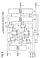
- Fig. 4 which shows a circuit diagram of the semiconductor integrated circuit disclosed in JP-A-08-170978 and US Patent 5,729,553, explanation will be made, by dividing the situation into a condition in which a function inherent to a semiconductor integrated circuit 1d is realized while exchanging various signals between an internal circuit of the semiconductor integrated circuit and an external circuit (this will be called a "normal mode” hereinafter), and another condition in which a function test of respective circuit blocks 81, 82 and 83 is conducted (this will be called a "test mode” hereinafter).
- An input terminal 3 receives an input signal DIN supplied in a parallel format of for example 64 bits, from an external circuit when the semiconductor integrated circuit 1d is in the normal mode. This input signal will be called a "normal input signal” hereinafter.
- An output terminal 7 outputs an output signal DOUT in the parallel format of for example 64 bits, to the external circuit when the semiconductor integrated circuit 1d is in the normal mode. This output signal will be called a "normal output signal” hereinafter.
- An input terminal 2 receives a testing input signal TIN supplied in a parallel format of for example 32 bits, from an external circuit in the test mode for the circuit block 82.
- the testing signal is of 64 bits
- the testing input signal is given by supplying first 32 bits at a first time, and then, remaining 32 bits at a second time.
- An output terminal 8 outputs a test output signal TOUT in the parallel format of for example 32 bits, to the external circuit in the test mode for the circuit block 82.
- This test output signal will be called a "test output” hereinafter.
- An input terminal 6 receives a clock signal CLK from a circuit external to the semiconductor integrated circuit 1d.
- Input terminals 4 and 5 respectively receive mode control signals SEL1 and SEL2 for switching between the normal mode of the semiconductor integrated circuit 1d and the test mode of the circuit block 82.
- the two mode control signals SEL1 and SEL2 are required in order to perform a control of multiplexors 21 and 22 and a control of multiplexors 25 and 26, independently of each other, in the test mode of the circuit block 82.
- the mode control signal SEL1 is set to select output signals S71 and S72 of the circuit block 81, and the mode control signal SEL2 is set to select output signals S76 and S77 of the circuit block 82.
- the normal input signal DIN of 64 bits given to the input terminal 3 from the external circuit is supplied to the circuit block 81.
- a first 32-bit portion input of the 64-bit normal input signal thus supplied is selected as the output signal S71 of the circuit block 81 by the multiplexor 21, and then, supplied as a selected output signal S73 to a flipflop 23 so that it is stored in the flipflop 23 in synchronism with the clock CLK.
- the first 32-bit portion input stored in the flipflop 23 is supplied as an output signal S75 to the circuit block 82 in synchronism with the clock CLK.
- the remaining second 32-bit portion input of the 64-bit normal input signal is selected as the output signal S72 of the circuit block 81 by the multiplexor 22, and then, supplied as a selected output signal S74 to a flipflop 24 so that it is stored in the flipflop 24 in synchronism with the clock CLK.
- the second 32-bit portion input signal S74 stored in the flipflop 24 is supplied to the circuit block 82 in synchronism with the clock CLK.
- An output signal S77 of the circuit block 82 corresponding to the second 32-bit portion input signal S74 is supplied through the multiplexor 26 to the circuit block 83.
- an output signal S76 of the circuit block 82 corresponding to the first 32-bit portion input is supplied through the multiplexor 25 to the circuit block 83.
- the result of the operation of the circuit block 83 is outputted to the output terminal 7 as the 64-bit output signal DOUT.
- the mode control signals are set to supply the testing input signal TIN to the circuit block 82.
- the mode control signal SEL1 is set to select an output signal S78 of the multiplexor 25 and an output signal S79 of the multiplexor 26, and the mode control signal SEL2 is set to select the testing input signal TIN and the output signal S75 of the flipflop 23.
- the first 32-bit portion input of the testing input signal TIN given through the input terminal 2 is selected by the multiplexor 25, and the output signal S78 of the multiplexor 25 is selected by the multiplexor 21 so that it is stored in the flipflop 23.
- the portion testing input signal TIN stored in the flipflop 23 in the first clock cycle is selected by the multiplexor 26, and the output signal S79 of the multiplexor 26 is selected by the multiplexor 22 to be supplied to the flipflop 24.
- the second 32-bit portion input of testing input signal TIN given through the input terminal 2 in the same second clock cycle is selected by the multiplexor 25, and the output signal S78 of the multiplexor 25 is selected by the multiplexor 21 so that it is stored in the flipflop 23 and then supplied to the circuit block 82.
- the input signal TIN is divided into the first 32-bit portion input and the second 32-bit portion input, which are supplied to the input terminal 2 in the named order, so that these portions are inputted into the circuit block 82 through different paths, respectively.
- the setting of the mode control signals is changed in order to observe the test result. Namely, the mode control signal SEL1 is set to select the output signal S78 of the multiplexor 25 and the output signal S79 of the multiplexor 26, and the mode control signal SEL2 is set to select the output signals S76 and S77 of the circuit block 82.
- the output signal S76 indicative of the test result of the circuit block 82 corresponding to the second 32-bit portion input is supplied through the multiplexor 25 and the multiplexor 21 and stored in the flipflop 23 during the period of one clock cycle.
- the output signal S77 indicative of the test result of the circuit block 82 corresponding to the first 32-bit portion input is supplied through the multiplexor 26 and the multiplexor 22 and stored in the flipflop 24 during the period of the same one clock cycle.
- the mode control signal SEL1 is set to select an output signal S78 of the multiplexor 25 and an output signal S79 of the multiplexor 26, and the mode control signal SEL2 is set to select the testing input signal TIN and the output signal S75 of the flipflop 23, again, so that the result of the test of the circuit block 82 stored in the flipflops 23 and 24 is shifted in the flipflops 23 and 24 cascade-connected in the form of a shift register.
- test result of the circuit block 82 stored in the flipflop 24 corresponding to the first 32-bit portion input is observed at the test output terminal 8
- test result of the circuit block 82 stored in the flipflop 23 corresponding to the second 32-bit portion input is selected as the output signal of the flipflop 23 by the multiplexor 26 and then selected by the multiplexor 22 to be stored in the flipflop 24, and the output of the flipflop is observed as the test result TOUT at the test output terminal 8
- a first problem is that, in the normal mode, since the flipflops exist in the input path from the circuit block 81 to the circuit block 82, the inputting of the signal from the circuit block 81 to the circuit block 82 can be performed only at a timing in synchronism with the clock, and therefore, the operation speed of the normal mode is low.
- a second problem is that, in the normal mode, since the multiplexors exist in the output path from the circuit block 82 to the circuit block 83, a delay occurs in the outputting from the circuit block 82 to the circuit block 83, and therefore, the operation speed is low.
- a third problem is that, in the test mode of the circuit block 82, since a plurality of multiplexors exists between the flipflops cascade-connected to constitute the shift register, a delay occurs in the path constituting the shift register, and therefore, the operation speed is low.
- Another object of the present invention is to provide a semiconductor integrated circuit capable of efficiently performing all function tests of a plurality of circuit blocks each realizing a predetermined function, and capable of minimizing the lowering of the circuit operation speed both in the normal mode and in the test mode.
- a semiconductor integrated circuit comprising a first circuit block constituting an input circuit, a second circuit block constituted of a predetermined function block, a third circuit block constituting an output circuit, the first, second and third circuit blocks being cascade-connected, and a testing additional means for performing a function test for the second circuit block, the testing additional means being provided only at an input side of the second circuit block, and the second circuit block being connected directly to the third circuit block through only interconnections.
- only one signal selection means for selecting an input signal is provided in a signal transfer path between a first output node of the first circuit block and a first input node of the second circuit block, and only one signal selection means for selecting an input signal is provided in a signal transfer path between a second output node of the first circuit block and a second input node of the second circuit block.
- a plurality of flipflops of the number corresponding to the number of the input nodes of the second circuit block provided for storing a testing signal when a testing signal is applied to the second circuit block and also for storing a test result signal when the test result signal is outputted from the second circuit block, are cascade-connected to constitute a shift register, so that the test result signal is serially outputted by a shifting action of the shift register, with only one signal selection means being interposed between each pair of adjacent flipflops of the shift register.
- the testing additional means includes a test input terminal for serially receiving the testing signal from an external circuit for the function test of the second circuit block, a test output terminal for serially outputting the test result signal so that the result of the function test of the second circuit block is observed externally, a clock terminal for receiving a clock signal from the external circuit, a first mode control terminal for receiving a first mode control signal from the external circuit.
- a second mode control terminal for receiving a second mode control signal from the external circuit, the first and second mode control signals being used for changing an operation condition in the test mode, a first multiplexor controlled by the first mode control signal for selectively outputting either a signal from the first output node of the second circuit block or a signal from the test input terminal, a first flipflop for holding the signal selected by the first multiplexor in synchronism with the clock signal, a second multiplexor controlled by the second mode control signal for selectively outputting either a signal from one of outputs of the first flipflop or a signal from the first output node of the first circuit block, a third multiplexor controlled by the first mode control signal for selectively outputting either a signal from the other output of the first flipflop or a signal from the second output node of the second circuit block, a second flipflop for holding the signal selected by the second multiplexor in synchronism with the clock signal, for outputting the selected signal to the test output terminal, and a fourth multiplexor controlled by the second mode control signal
- the testing additional means cascade-connects the first multiplexor, the first flipflop, the second multiplexor and the second flipflop in the named order to cause them to constitute one shift register, so that a first testing signal inputted from the test input terminal at a first clock and a second testing signal inputted from the test input terminal at a second clock are serially inputted to the shift register and held in the shift register, and the second testing signal held in the first flipflop at the second clock is supplied through the second multiplexor to the first input node of the second circuit block, and the first testing signal held in the second flipflop at the second clock is supplied through the fourth multiplexor to the second input node of the second circuit block, and wherein, of the test result of the function test of the second circuit block, a first partial output is held in the first flipflop through the first multiplexor at a third clock, and simultaneously, a second partial output is held in the second flipflop through the third multiplexor, and thereafter, the first flipflop and the second flipflop
- the number of the input nodes of the second circuit block is larger than the number of the output nodes of the second circuit block by at least one, and the first circuit block includes a third output node, and the second circuit block includes a third input node.
- the testing additional means further includes a fifth multiplexor controlled by the first mode control signal for selectively outputting either a signal from the other output of the second flipflop or the signal from the second output node of the second circuit block, a third flipflop for holding the signal selected by the fifth multiplexor in synchronism with the clock signal, for outputting the selected signal to the test output terminal, and a sixth multiplexor controlled by the second mode control signal for selectively outputting either a signal from one of outputs of the third flipflop or a signal from the third output node of the first circuit block, the third multiplexor receiving the signal from the first output node of the second circuit block in place of the signal from the second output node of the second circuit block, so that the number of the input nodes of the second circuit block is adapted to the number of the output nodes of the second circuit block.
- the number of the output nodes of the second circuit block is larger than the number of the input nodes of the second circuit block by at least one, and the second circuit block includes a third output node.
- the testing additional means further includes an exclusive-OR circuit of the number smaller than the number of the input nodes of the second circuit block by at least one, and the third multiplexor other than the first multiplexor, of the multiplexors located at an input side of the first and second flipflops, receives, in place of the signal from the second output node of the second circuit block, an output signal of the exclusive-OR circuit receiving signals which are outputted from the second and third output nodes of the second circuit block, so that the number of the output nodes of the second circuit block is adapted to the number of the input nodes of the second circuit block.
- each of the input signal given to the first circuit block and the testing signal given to the testing additional means is a signal of an arbitrary bit number
- each of the output nodes of the first circuit block and the input nodes of the second circuit block is a signal of the same arbitrary bit number obtained by dividing the arbitrary bit number
- each of the output nodes of the second circuit block is a signal of the bit number including the same arbitrary bit number and obtained by dividing the arbitrary bit number.
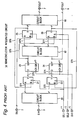
- Fig. 1 is a block diagram of a first embodiment of the semiconductor integrated circuit in accordance with the present invention.
- the semiconductor integrated circuit is generally designated with Reference Numeral la, and comprising external input terminals 2, 3, 4, 5 and 6, external output terminals 7 and 8, a first circuit block 11, a second circuit block 12, a third circuit block 13, and a testing additional circuit, which are connected as shown.
- the first circuit block 11 mainly constitutes an input circuit and has an input node connected to the external input terminal 3, a first output node for outputting an output signal S1, and a second output node for outputting an output signal S2.
- the second circuit block 12 is constituted of a predetermined function block, for example, a CPU, a ROM, or a RAM, or alternatively, a random logic circuit.
- This second circuit block 12 includes a first input node, a second input node, a first output node for outputting an output signal S5, and a second output node for outputting an output signal S6.
- the third circuit block 13 mainly constitutes an output circuit and has a first input node receiving the output signal S5, a second input node receiving the output signal S6, and an output node for outputting an output signal DOUT to the external output terminal 7.
- the testing additional circuit is located between the circuit block 11 and the circuit block 12 in order to test the circuit block 12.
- the testing additional circuit includes a multiplexor 21 having a pair of input nodes A and B and an output node Y, a flipflop 23 receiving at a data input node D a signal S7 from the output node Y of the multiplexor 21 to hold it in synchronism with a clock signal, and another multiplexor 25 having an input node B receiving a Q (non-inverting) output signal S9 of the flipflop 23, another input node A receiving the first output signal S1 of the circuit block 11 and an output node Y for supplying a selected signal S3 to the first input node of the circuit block 12.
- the testing additional circuit also includes a multiplexor 22 having a pair of input nodes A and B and an output node Y, a flipflop 24 receiving at a data input node D a signal S8 from the output node Y of the multiplexor 22 to hold it in synchronism with a clock signal, and a multiplexor 26 having an input node B receiving a Q (non-inverting) output signal S10 of the flipflop 24, another input node A receiving the second output signal S2 of the circuit block 11 and an output node Y for supplying a selected signal S4 to the second input node of the circuit block 12.
- a multiplexor 22 having a pair of input nodes A and B and an output node Y
- a flipflop 24 receiving at a data input node D a signal S8 from the output node Y of the multiplexor 22 to hold it in synchronism with a clock signal
- a multiplexor 26 having an input node B receiving a Q (non-inverting)
- the external input terminal 3 and the external output terminal 7 are adapted for a parallel signal format of for example 64 bits
- the external input terminal 2, the external output terminal 8, and the signals S1, S2, S3, S4, S5, S6, S7, S8, S9 and S10 are adapted for a parallel signal format of for example 32 bits which are obtained by halving the 64 bits.
- the drawing only one bit of these terminals and these signals is shown for simplification of the drawing and for making it easier to understand.
- the input terminal 3 receives a normal input signal DIN supplied from an external circuit when the semiconductor integrated circuit 1a is in a normal mode. This input signal is assumed to be given in a parallel format of for example 64 bits, similarly to the prior art example mentioned hereinbefore.
- the input terminal 2 receives a testing input signal TIN supplied from an external circuit in the test mode for the circuit block 12.
- the input terminals 4 and 5 respectively receive mode control signals SEL1 and SEL2 for switching between the normal mode of the semiconductor integrated circuit 1a and the test mode of the circuit block 12.
- the input terminal 6 receives a clock signal CLK from a circuit external to the semiconductor integrated circuit la.
- the output terminal 7 outputs the normal output signal DOUT to the external circuit in the normal mode.
- the output terminal 8 outputs a test output so that the test result is observed at an external in the test mode for the circuit block 82.
- the two mode control signals SEL1 and SEL2 are required in order to perform a control of the multiplexors 21 and 22 and a control of the multiplexors 25 and 26, independently of each other, in the test mode of the circuit block 12.
- the mode control signal SEL2 is set to select the output signals S1 and S2 of the circuit block 11.
- the mode control signal SEL1 can be set at an arbitrary value.
- the normal input signal DIN supplied through the input terminal 3 is applied to the circuit block 11.
- the output signal S1 of the circuit block 11 is supplied through only the multiplexor 25 to the circuit block 12.
- the output signal S2 of the circuit block 11 is supplied through only the multiplexor 26 to the circuit block 12.
- the output signal S5 of the circuit block 12 is supplied directly to the first input node of the circuit block 13 through no logic gate.
- the output signal S6 of the circuit block 12 is supplied directly to the second input node of the circuit block 13 through no logic gate.
- the normal output signal DOUT of the circuit block 13 is outputted to the output terminal 7.
- the mode control signals are set to supply the testing input signal TIN to the circuit block 12.
- the mode control signal SEL1 is set to select the testing input signal TIN and an output signal S11 outputted from an inverting output QB of the flipflop 23, and the mode control signal SEL2 is set to select the signals S9 and S10.
- the first test input (of 32 bits) supplied as the testing input signal TIN is selected by the multiplexor 21 and stored in the flipflop 23 in synchronism with the clock CLK.
- the test input stored in the flipflop 23 is selected as the output signal S11 of the flipflop 23 by the multiplexor 22, and stored in the flipflop 24 in synchronism with the clock CLK.
- the test input stored in the flipflop 24 is selected by the multiplexor 26 and supplied as the output signal S4 of the flipflop 24 to the second input node of the circuit block 12.
- the second test input (of 32 bits) supplied as the testing input signal TIN is selected by the multiplexor 21 and stored in the flipflop 23 in synchronism with the clock CLK. Furthermore, the test input stored in the flipflop 23 is selected as the output signal S9 of the flipflop 23 by the multiplexor 25, and the signal selected by the multiplexor 25 is supplied as the output signal S3 to the first input node of the circuit block 12.
- the mode control signals are set again in order to observe the test result.
- the mode control signal SEL1 is set to select the output signals S5 and S6 which are outputted from the first output node and the second output node of the circuit block 12, respectively.
- the mode control signal SEL2 is set to select the output signal S9 of the flipflop 23 and the output signal S10 of the flipflop 24.
- the output signal S5 indicative of the test result, outputted from the first output node of the circuit block 12, is selected by the multiplexor 21 during one clock cycle, and stored in the flipflop 23 in synchronism with the clock signal CLK.
- the output signal S6 indicative of the test result, outputted from the second output node of the circuit block 12, is selected by the multiplexor 22 during the same one clock cycle, and stored in the flipflop 24 in synchronism with the clock signal CLK.
- the mode control signal SEL1 is set to select the testing input signal TIN and an output signal S11 outputted from the inverting output QB of the flipflop 23, so that the test result of the circuit block 12 stored in the flipflops 23 and 24 is shifted by a shifting operation of the flipflops 23 and 24 cascade-connected to constitute the shift register because the multiplexor 22 selects the output signal S11 of the flipflop 23.
- test result TOUT stored in the flipflop 24 is observed from an inverting output QB of the flipflop 24 at the output terminal 8, and in a second clock cycle, the test result TOUT stored in the flipflop 23 is shifted to the flipflop 24, so that the inverting output QB of the flipflop 24 can be observed at the output terminal 8.
- the operation for supplying the testing input signal TIN through the test input terminal 2, for causing an internal circuit of the circuit block 12 to operate, and for observing the test result TOUT at the test output terminal 8, is completed with five clock cycles.
- the circuit such as the flipflop operating in synchronism with the clock, or a random logic circuit, does not exist in the signal transfer path between the circuit blocks 11 and 12, and since there exist only the multiplexor 25 for the signal selection between the first output node of the circuit block 11 and the first input node of the circuit block 12, and the multiplexor 26 for the signal selection between the second output node of the circuit block 11 and the second input node of the circuit block 12, the signal delay is minimized.
- the second embodiment of the semiconductor integrated circuit in accordance with the present invention is generally designated with Reference Numeral 1b, and is different from the first embodiment in that a first circuit block 51 comparable to the circuit block 11, has output nodes of the number which is larger than that of the circuit block 11 by at least one, and the additional output node of the first circuit block 51 is called a third output node, and a second circuit block 52 comparable to the circuit block 12, has input nodes of the number which is larger than that of the circuit block 12 by at least one, and the additional output node of the second circuit block 52 is called a third input node, so that the testing additional circuit is scaled up by increasing the number of output nodes of the first circuit block and the number of the input nodes of the second circuit block.
- the testing additional circuit of the semiconductor integrated circuit 1b includes a multiplexor 21 having an input node A connected to the input terminal 2 so as to receive the testing input signal TIN, another input node B receiving a first output signal S5 of the circuit block 52, and an output node Y for outputting a selected signal, a flipflop 23 receiving at a data input node D a signal S7 from the output node Y of the multiplexor 21 to hold it in synchronism with a clock signal CLK, and another multiplexor 25 having an input node B receiving a Q (non-inverting) output signal S9 of the flipflop 23, another input node A receiving the first output signal S1 of the circuit block 11 and an output node Y for supplying a selected signal S3 to the first input node of the circuit block 52.
- a multiplexor 21 having an input node A connected to the input terminal 2 so as to receive the testing input signal TIN, another input node B receiving a first output signal S5 of the circuit block 52, and an output
- the testing additional circuit also includes a multiplexor 22 having an input node A for receiving an output signal S11 from an inverting output QB of the flipflop 23, another input node B receiving a first output signal S5 of the circuit block 52, and an output node Y for supplying a selected signal, a flipflop 24 receiving at a data input node D a signal S8 from the output node Y of the multiplexor 22 to hold it in synchronism with the clock signal CLK, and a multiplexor 26 having an input node B receiving a Q (non-inverting) output signal S10 of the flipflop 24, another input node A receiving the second output signal S2 of the circuit block 51 and an output node Y for supplying a selected signal S4 to the second input node of the circuit block 52.
- a multiplexor 22 having an input node A for receiving an output signal S11 from an inverting output QB of the flipflop 23, another input node B receiving a first output signal S5 of the circuit block 52, and an output
- the testing additional circuit furthermore includes a multiplexor 27 having an input node A for receiving an output signal S16 from an inverting output QB of the flipflop 24, another input node B receiving a second output signal S6 of the circuit block 52, and an output node Y for supplying a selected signal, a flipflop 28 receiving at a data input node D a signal S14 from the output node Y of the multiplexor 27 to hold it in synchronism with the clock signal CLK, and a multiplexor 29 having an input node B receiving a Q (non-inverting) output signal S15 of the flipflop 28, another input node A receiving the third output signal S12 of the circuit block 51 and an output node Y for supplying a selected signal S13 to the third input node of the circuit block 52.
- a multiplexor 27 having an input node A for receiving an output signal S16 from an inverting output QB of the flipflop 24, another input node B receiving a second output signal S6 of the circuit block 52, and an
- the mode control signal SEL2 is set to select the output signals S1, S2 and S12 of the circuit block 51.
- the mode control signal SEL1 can be set at an arbitrary value.
- the normal input signal DIN supplied through the input terminal 3 is applied to the circuit block 51.
- the output signal S1 outputted from the first output node of the circuit block 51 is selected by only the multiplexor 25 and supplied as the output signal S3 to the first input node of the circuit block 52.
- the output signal S2 outputted from the second output node of the circuit block 51 is selected by only the multiplexor 26 and supplied as the output signal S4 to the second input node of the circuit block 52.
- the output signal S12 outputted from the third output node of the circuit block 51 is selected by only the multiplexor 29 and supplied as the output signal S13 to the third input node of the circuit block 52.
- the output signal S5 of the circuit block 52 is supplied directly to the first input node of the circuit block 13 through no logic gate.
- the output signal S6 of the circuit block 52 is supplied directly to the second input node of the circuit block 13 through no logic gate.
- the normal output signal DOUT of the circuit block 13 is outputted to the output terminal 7.
- the mode control signals are set to supply the testing input signal TIN to the circuit block 52.
- the mode control signal SEL1 is set to select the testing input signal TIN, the output signal S11 of the flipflop 23, and the output signal S16 of the flipflop 24, and the mode control signal SEL2 is set to select the signal S9 of the flipflop 23, the signal S10 of the flipflop 24, and the signal S15 of the flipflop 28.
- the first testing input signal TIN supplied through the input terminal 2 is selected by the multiplexor 21 and the output signal S7 of the multiplexor 21 is stored in the flipflop 23.
- the testing input signal stored in the flipflop 23 is selected as the output signal S11 by the multiplexor 22, and the output signal S8 of the multiplexor 22 is stored in the flipflop 24.
- the second testing input signal TIN supplied through the input terminal 2 is selected by the multiplexor 21 and the output signal S7 of the multiplexor 21 is stored in the flipflop 23.
- the testing input signal stored in the flipflop 24 is selected as the output signal S16 by the multiplexor 27, and the output signal S14 of the multiplexor 27 is stored in the flipflop 28. Furthermore, the testing input signal stored in the flipflop 23 is selected as the output signal S11 by the multiplexor 22, and the output signal S8 of the multiplexor 22 is stored in the flipflop 24. In the same third clock cycle, the third testing input signal TIN supplied through the input terminal 2 is selected by the multiplexor 21 and the output signal S7 of the multiplexor 21 is stored in the flipflop 23.
- the three testing input signals stored in the three flipflops 23, 24 and 28, respectively, are selected by the multiplexors 25, 26 and 29, respectively, so as to be supplied as the output signals S3, S4 and S13 to the first, second and third input nodes of the circuit block 53, respectively.
- the mode control signals are set again in order to observe the test result.
- the mode control signal SEL1 is set to select the output signals S5 and S6 which are outputted from the first output node and the second output node of the circuit block 52, respectively.
- the mode control signal SEL2 is set to select the output signal S9 of the flipflop 23, the output signal S10 of the flipflop 24 and the output signal S15 of the flipflop 28.
- the output signal S5 indicative of the test result, outputted from the first output node of the circuit block 52, is selected by the multiplexor 21 during one clock cycle, and the output signal S7 of the multiplexor 21 is stored in the flipflop 23 in synchronism with the clock signal CLK. Simultaneously, the output signal S5 is selected by the multiplexor 22, and the output signal S8 of the multiplexor 22 is stored in the flipflop 24.
- the output signal S6 indicative of the test result, outputted from the second output node of the circuit block 52, is selected by the multiplexor 27 during the same one clock cycle, and the output signal S14 of the multiplexor 27 is stored in the flipflop 28.
- test result signals TOUT of the circuit block 52, stored in the flipflops 23, 24 and 28, respectively, can be observed at the output terminal 8 with three clock cycles by setting the mode control signals again to the effect that the flipflops 23, 24 and 28 are cascaded-connected by the multiplexors 21, 22 and 27 so as to constitute a shift register, and the test result signals stored in the flipflops 23, 24 and 28 is outputted by a shifting operation of the shift register.
- both of the test results stored in the flipflops 23 and 24 indicate the test result S5 of the circuit block 52, it is sufficient if either of the contents stored in the flipflops 23 and 24 is selected as the test result.
- test result S5 of the circuit block 52 is connected in common to the multiplexors 21 and 22 other than the multiplexor 27, so that if the test result signals S5 and S6 are two output signals as in this embodiment, the input signals are similarly made to two signals.
- the circuit such as the flipflop operating in synchronism with the clock, or a random logic circuit, does not exist in the signal transfer path between the circuit blocks 51 and 52, and since there exist only the multiplexor 25 for the signal selection between the first output node of the circuit block 51 and the first input node of the circuit block 52, the multiplexor 26 for the signal selection between the second output node of the circuit block 51 and the second input node of the circuit block 52, and the multiplexor 29 for the signal selection between the third output node of the circuit block 51 and the third input node of the circuit block 52, the signal delay is minimized.
- FIG. 3 is a block diagram of the third embodiment of the semiconductor integrated circuit in accordance with the present invention.
- elements similar to those shown in Fig. 1 are given the same Reference Numerals, and explanation thereof will be omitted for simplification of description.
- the third embodiment of the semiconductor integrated circuit is different from the first embodiment, in that the number of output nodes of a second circuit block 62 is larger than that of the second circuit block 12 by at least one, and correspondingly, the number of input nodes of a third circuit block 63 is larger than that of the third circuit block 13 by at least one, and in that there is added an exclusive-OR circuit 70 for receiving output signals S17 and S18 outputted from the second output node and the added third output node of the circuit block 62, respectively, an output of the exclusive-OR circuit 70 being connected to the input node B of the multiplexor 22.
- the number of the exclusive-OR circuit 70 is smaller than the number of input nodes of the circuit block 62 by at least one.
- the exclusive-OR circuit 70 is provided to adjust between the output node number and the input node number of the circuit block 62. Therefore, when the output node number of the circuit block 62 is much larger than the input node number of the circuit block 62, a plurality of exclusive-OR circuits are provided each of which receives each two of the output node signals of the circuit block 62, other than the output node signal S5, and furthermore, a exclusive-OR circuit or exclusive-OR circuits are added and connected to constitute a tree structure circuitry so that the number of exclusive-OR circuit at a final stage becomes one.
- the mode control signal SEL2 is set to select the output signals S1 and S2 of the circuit block 11.
- the mode control signal SEL1 can be set at an arbitrary value.
- the normal input signal DIN supplied through the input terminal 3 is applied to the circuit block 11.
- the output signal S1 of the circuit block 11 is supplied through only the multiplexor 25 to the circuit block 62.
- the output signal S2 of the circuit block 11 is supplied through only the multiplexor 26 to the circuit block 62.
- the output signals S5, S17 and S18 of the circuit block 62 are supplied directly to the circuit block 63 through no logic gate.
- the normal output signal DOUT of the circuit block 63 is outputted to the output terminal 7.
- the mode control signals are set to supply the testing input signal TIN to the circuit block 62.
- the mode control signal SEL1 is set to select the testing input signal TIN and the output signal S11 of the flipflop 23
- the mode control signal SEL2 is set to select the output signal S9 of the flipflop 23 and the output signal S10 of the flipflop 24.
- the first testing input signal TIN supplied from the input terminal 2 is selected by the multiplexor 21 and the output signal S7 of the multiplexor 21 is stored in the flipflop 23.
- the first testing input signal stored in the flipflop 23 is selected as the output signal S11 of the flipflop 23 by the multiplexor 22, and stored in the flipflop 24.
- the second testing input signal TIN supplied from the input terminal 2 is selected by the multiplexor 21 and stored in the flipflop 23.
- the two testing input signals TIN stored in the two flipflops 23 and 24 are selected by the multiplexors 25 and 26, respectively, and supplied as the output signals S3 and S4 to the circuit block 62.
- the mode control signals are set again in order to observe the test result.
- the mode control signal SEL1 is set to select the output signal S5 of the circuit block 62 and the output signal S19 of the exclusive-OR circuit 70, respectively.
- the mode control signal SEL2 is set to select the output signal S9 of the flipflop 23 and the output signal S10 of the flipflop 24.
- the output signal S5 indicative of the test result, outputted from the circuit block 62, is selected by the multiplexor 21 during one clock cycle, and stored in the flipflop 23.
- the output signals S17 and S18 indicative of the test result, outputted from the circuit block 62 are supplied to the exclusive-OR circuit 70, and a coincidence output S19 outputted from the exclusive-OR circuit 70 is selected by the multiplexor 22 and stored in the flipflop 24.
- the mode control signal SEL1 is set to select the testing input signal TIN and the output signal S11 of the flipflop 23, so that the test result TOUT of the circuit block 62 stored in the flipflops 23 and 24 is shifted by a shifting operation of the flipflops 23 and 24 cascade-connected by the multiplexor 22 to constitute the shift register, so that the test result TOUT can be observed at the output terminal 8 with two clock cycles.
- the circuit such as the flipflop operating in synchronism with the clock, or a random logic circuit, does not exist in the signal transfer path between the circuit blocks 11 and 62, and since there exist only the multiplexor 25 for the signal selection between the first output node of the circuit block 11 and the first input node of the circuit block 62, and the multiplexor 26 for the signal selection between the second output node of the circuit block 11 and the second input node of the circuit block 62, the signal delay is minimized.
- the semiconductor integrated circuit in accordance with the present invention comprises a first circuit block constituting an input circuit, a second circuit block constituted of a predetermined function block, a third circuit block constituting an output circuit, the first, second and third circuit blocks being cascade-connected, and a testing additional circuit for performing a function test for the second circuit block, the testing additional circuit being provided only at an input side of the second circuit block, and the second circuit block being connected directly to the third circuit block through only interconnections.
- only one signal selection means for selecting an input signal is provided in a signal transfer path between a first output node of the first circuit block and a first input node of the second circuit block, and only one signal selection means for selecting an input signal is provided in a signal transfer path between a second output node of the first circuit block and a second input node of the second circuit block.
- a plurality of flipflops of the number corresponding to the number of the input nodes of the second circuit block provided for storing a testing signal when a testing signal is applied to the second circuit block and also for storing a test result signal when the test result signal is outputted from the second circuit block, are cascade-connected to constitute a shift register, so that the test result signal is serially outputted by a shifting action of the shift register, with only one signal selection means being interposed between each pair of adjacent flipflops of the shift register.
- a first advantage is that, in the normal operation, the signal is supplied from the first circuit block to the second circuit block, independently of the timing of the clock, because only the multiplexor is interposed in the signal transfer path from the first circuit block to the second circuit block.
- a second advantage is that, in the normal operation, the signal is transferred from the first circuit block to the second circuit block, with no substantial delay, and therefore, the operation speed can be improved, because the first circuit block is connected to the second circuit block without a logic gate such as a random logic.
- a third advantage is that, in the test mode of the second circuit block, the delay of the signal transfer between the first flipflop and the second flipflop which constitute the shift register can be reduced, and therefore, the operation speed can be improved, because only one multiplexor is interposed between the first flipflop and the second flipflop which constitute the shift register.
Landscapes
- Engineering & Computer Science (AREA)
- General Engineering & Computer Science (AREA)
- Physics & Mathematics (AREA)
- General Physics & Mathematics (AREA)
- Tests Of Electronic Circuits (AREA)
- Semiconductor Integrated Circuits (AREA)
- Test And Diagnosis Of Digital Computers (AREA)
- Testing Or Measuring Of Semiconductors Or The Like (AREA)
Applications Claiming Priority (2)
| Application Number | Priority Date | Filing Date | Title |
|---|---|---|---|
| JP41498 | 1998-01-05 | ||
| JP00041498A JP3145976B2 (ja) | 1998-01-05 | 1998-01-05 | 半導体集積回路 |
Publications (2)
| Publication Number | Publication Date |
|---|---|
| EP0939320A2 true EP0939320A2 (fr) | 1999-09-01 |
| EP0939320A3 EP0939320A3 (fr) | 2000-01-05 |
Family
ID=11473149
Family Applications (1)
| Application Number | Title | Priority Date | Filing Date |
|---|---|---|---|
| EP99100078A Withdrawn EP0939320A3 (fr) | 1998-01-05 | 1999-01-05 | Procédé et dispositif d'essai de circuit à semiconducteur |
Country Status (5)
| Country | Link |
|---|---|
| US (1) | US6370663B1 (fr) |
| EP (1) | EP0939320A3 (fr) |
| JP (1) | JP3145976B2 (fr) |
| KR (1) | KR19990066894A (fr) |
| CN (1) | CN1141594C (fr) |
Families Citing this family (8)
| Publication number | Priority date | Publication date | Assignee | Title |
|---|---|---|---|---|
| US7389452B2 (en) * | 2004-06-29 | 2008-06-17 | Electronics For Imaging, Inc. | Methods and apparatus for monitoring internal signals in an integrated circuit |
| KR100714482B1 (ko) * | 2005-07-11 | 2007-05-04 | 삼성전자주식회사 | 반도체 장치, 테스트 기판, 반도체 장치의 테스트 시스템및 반도체 장치의 테스트 방법 |
| CN100490106C (zh) * | 2005-09-23 | 2009-05-20 | 矽统科技股份有限公司 | 判断集成电路处理速度的测试系统与测试方法 |
| JP2011149775A (ja) * | 2010-01-20 | 2011-08-04 | Renesas Electronics Corp | 半導体集積回路及びコアテスト回路 |
| US8627160B2 (en) * | 2010-04-21 | 2014-01-07 | Lsi Corporation | System and device for reducing instantaneous voltage droop during a scan shift operation |
| US8738979B2 (en) * | 2012-03-30 | 2014-05-27 | Lsi Corporation | Methods and structure for correlation of test signals routed using different signaling pathways |
| US9183105B2 (en) | 2013-02-04 | 2015-11-10 | Alcatel Lucent | Systems and methods for dynamic scan scheduling |
| CN113447799B (zh) * | 2020-03-27 | 2022-06-14 | 阿里巴巴集团控股有限公司 | 集成电路、信息收集方法、设备 |
Family Cites Families (17)
| Publication number | Priority date | Publication date | Assignee | Title |
|---|---|---|---|---|
| FR2330014A1 (fr) | 1973-05-11 | 1977-05-27 | Ibm France | Procede de test de bloc de circuits logiques integres et blocs en faisant application |
| JPS5255874A (en) | 1975-10-31 | 1977-05-07 | Toshiba Corp | Integrated circuit |
| US4703257A (en) | 1984-12-24 | 1987-10-27 | Hitachi, Ltd. | Logic circuit having a test data scan circuit |
| JPH0672911B2 (ja) | 1985-05-29 | 1994-09-14 | 株式会社東芝 | システムlsi |
| JPS62261168A (ja) | 1986-05-07 | 1987-11-13 | Nec Corp | 半導体集積回路の設計評価方法 |
| JPH01192161A (ja) | 1988-01-27 | 1989-08-02 | Nec Corp | 半導体装置 |
| JPH04370775A (ja) | 1991-06-19 | 1992-12-24 | Nec Corp | Lsi試験システム |
| JP2770617B2 (ja) * | 1991-09-05 | 1998-07-02 | 日本電気株式会社 | テスト回路 |
| JPH05312920A (ja) | 1992-05-13 | 1993-11-26 | Hitachi Ltd | 半導体集積回路 |
| JPH05341014A (ja) | 1992-06-10 | 1993-12-24 | Oki Electric Ind Co Ltd | 半導体モジュール装置、半導体モジュール単体及び試験方法 |
| JP3304399B2 (ja) * | 1992-06-12 | 2002-07-22 | 日本電気株式会社 | 半導体集積論理回路 |
| JPH06289106A (ja) | 1993-04-06 | 1994-10-18 | Sony Corp | 集積回路装置及び集積回路装置の製造方法 |
| JP3453460B2 (ja) | 1994-08-29 | 2003-10-06 | 松下電器産業株式会社 | 半導体集積回路 |
| US5729553A (en) * | 1994-08-29 | 1998-03-17 | Matsushita Electric Industrial Co., Ltd. | Semiconductor integrated circuit with a testable block |
| TW307927B (fr) | 1994-08-29 | 1997-06-11 | Matsushita Electric Industrial Co Ltd | |
| JPH07167923A (ja) | 1994-10-03 | 1995-07-04 | Oki Electric Ind Co Ltd | テスト用回路付集積回路 |
| JPH112665A (ja) | 1997-06-13 | 1999-01-06 | Nec Corp | Lsi試験方式 |
-
1998
- 1998-01-05 JP JP00041498A patent/JP3145976B2/ja not_active Expired - Fee Related
- 1998-12-30 KR KR1019980061577A patent/KR19990066894A/ko not_active Abandoned
-
1999
- 1999-01-05 EP EP99100078A patent/EP0939320A3/fr not_active Withdrawn
- 1999-01-05 US US09/225,434 patent/US6370663B1/en not_active Expired - Fee Related
- 1999-01-05 CN CNB991000226A patent/CN1141594C/zh not_active Expired - Fee Related
Also Published As
| Publication number | Publication date |
|---|---|
| JPH11194152A (ja) | 1999-07-21 |
| CN1141594C (zh) | 2004-03-10 |
| JP3145976B2 (ja) | 2001-03-12 |
| CN1229925A (zh) | 1999-09-29 |
| US6370663B1 (en) | 2002-04-09 |
| EP0939320A3 (fr) | 2000-01-05 |
| KR19990066894A (ko) | 1999-08-16 |
Similar Documents
| Publication | Publication Date | Title |
|---|---|---|
| US7290190B2 (en) | Semiconductor integrated circuit with a test circuit | |
| US4799004A (en) | Transfer circuit for operation test of LSI systems | |
| US6819140B2 (en) | Self-synchronous logic circuit having test function and method of testing self-synchronous logic circuit | |
| US5130647A (en) | Scan test circuit and semiconductor integrated circuit device using the same | |
| EP0438322A2 (fr) | Registre à décalage à rebouclage linéaire | |
| US20030056183A1 (en) | Scan test circuit, and semiconductor integrated circuit including the circuit | |
| US4995039A (en) | Circuit for transparent scan path testing of integrated circuit devices | |
| US5077740A (en) | Logic circuit having normal input/output data paths disabled when test data is transferred during macrocell testing | |
| JPS63243890A (ja) | 半導体集積回路装置 | |
| US5457698A (en) | Test circuit having a plurality of scan latch circuits | |
| EP0939320A2 (fr) | Procédé et dispositif d'essai de circuit à semiconducteur | |
| JPH0627776B2 (ja) | 半導体集積回路装置 | |
| KR100336328B1 (ko) | 반도체집적회로 | |
| JP2638281B2 (ja) | スキャンパス回路 | |
| KR910000608B1 (ko) | 반도체 집적회로장치 | |
| US4913557A (en) | Intergrated logic circuit having testing function circuit formed integrally therewith | |
| KR100188819B1 (ko) | 디지탈 필터 | |
| JPH01110274A (ja) | 試験回路 | |
| KR20030030850A (ko) | 논리 회로 테스트용 스캔 패스 회로 및 이것을 구비한집적 회로 장치 | |
| US6118296A (en) | Semiconductor integrated logic circuit | |
| US6898748B1 (en) | Test circuit method and apparatus | |
| KR100313202B1 (ko) | 매크로용테스트회로 | |
| US7373570B2 (en) | LSI device having scan separators provided in number reduced from signal lines of combinatorial circuits | |
| KR19990077716A (ko) | 집적회로용 테스트 패턴을 발생시키는 방법 | |
| US20020053055A1 (en) | Semiconductor device having a test mode |
Legal Events
| Date | Code | Title | Description |
|---|---|---|---|
| PUAI | Public reference made under article 153(3) epc to a published international application that has entered the european phase |
Free format text: ORIGINAL CODE: 0009012 |
|
| AK | Designated contracting states |
Kind code of ref document: A2 Designated state(s): DE FR GB |
|
| AX | Request for extension of the european patent |
Free format text: AL;LT;LV;MK;RO;SI |
|
| PUAL | Search report despatched |
Free format text: ORIGINAL CODE: 0009013 |
|
| AK | Designated contracting states |
Kind code of ref document: A3 Designated state(s): AT BE CH CY DE DK ES FI FR GB GR IE IT LI LU MC NL PT SE |
|
| AX | Request for extension of the european patent |
Free format text: AL;LT;LV;MK;RO;SI |
|
| 17P | Request for examination filed |
Effective date: 20000406 |
|
| AKX | Designation fees paid |
Free format text: DE FR GB |
|
| RAP1 | Party data changed (applicant data changed or rights of an application transferred) |
Owner name: NEC ELECTRONICS CORPORATION |
|
| STAA | Information on the status of an ep patent application or granted ep patent |
Free format text: STATUS: THE APPLICATION HAS BEEN WITHDRAWN |
|
| 18W | Application withdrawn |
Effective date: 20031027 |