EP0952545A1 - Carte a circuit integre - Google Patents
Carte a circuit integre Download PDFInfo
- Publication number
- EP0952545A1 EP0952545A1 EP98947891A EP98947891A EP0952545A1 EP 0952545 A1 EP0952545 A1 EP 0952545A1 EP 98947891 A EP98947891 A EP 98947891A EP 98947891 A EP98947891 A EP 98947891A EP 0952545 A1 EP0952545 A1 EP 0952545A1
- Authority
- EP
- European Patent Office
- Prior art keywords
- reinforcing member
- card
- insulating substrate
- card according
- reinforcing
- Prior art date
- Legal status (The legal status is an assumption and is not a legal conclusion. Google has not performed a legal analysis and makes no representation as to the accuracy of the status listed.)
- Granted
Links
Images


Classifications
-
- G—PHYSICS
- G06—COMPUTING OR CALCULATING; COUNTING
- G06K—GRAPHICAL DATA READING; PRESENTATION OF DATA; RECORD CARRIERS; HANDLING RECORD CARRIERS
- G06K19/00—Record carriers for use with machines and with at least a part designed to carry digital markings
- G06K19/06—Record carriers for use with machines and with at least a part designed to carry digital markings characterised by the kind of the digital marking, e.g. shape, nature, code
- G06K19/067—Record carriers with conductive marks, printed circuits or semiconductor circuit elements, e.g. credit or identity cards also with resonating or responding marks without active components
- G06K19/07—Record carriers with conductive marks, printed circuits or semiconductor circuit elements, e.g. credit or identity cards also with resonating or responding marks without active components with integrated circuit chips
- G06K19/077—Constructional details, e.g. mounting of circuits in the carrier
- G06K19/07745—Mounting details of integrated circuit chips
- G06K19/07747—Mounting details of integrated circuit chips at least one of the integrated circuit chips being mounted as a module
-
- G—PHYSICS
- G06—COMPUTING OR CALCULATING; COUNTING
- G06K—GRAPHICAL DATA READING; PRESENTATION OF DATA; RECORD CARRIERS; HANDLING RECORD CARRIERS
- G06K19/00—Record carriers for use with machines and with at least a part designed to carry digital markings
- G06K19/06—Record carriers for use with machines and with at least a part designed to carry digital markings characterised by the kind of the digital marking, e.g. shape, nature, code
- G06K19/067—Record carriers with conductive marks, printed circuits or semiconductor circuit elements, e.g. credit or identity cards also with resonating or responding marks without active components
- G06K19/07—Record carriers with conductive marks, printed circuits or semiconductor circuit elements, e.g. credit or identity cards also with resonating or responding marks without active components with integrated circuit chips
- G06K19/077—Constructional details, e.g. mounting of circuits in the carrier
- G06K19/0772—Physical layout of the record carrier
- G06K19/07728—Physical layout of the record carrier the record carrier comprising means for protection against impact or bending, e.g. protective shells or stress-absorbing layers around the integrated circuit
-
- G—PHYSICS
- G06—COMPUTING OR CALCULATING; COUNTING
- G06K—GRAPHICAL DATA READING; PRESENTATION OF DATA; RECORD CARRIERS; HANDLING RECORD CARRIERS
- G06K19/00—Record carriers for use with machines and with at least a part designed to carry digital markings
- G06K19/06—Record carriers for use with machines and with at least a part designed to carry digital markings characterised by the kind of the digital marking, e.g. shape, nature, code
- G06K19/067—Record carriers with conductive marks, printed circuits or semiconductor circuit elements, e.g. credit or identity cards also with resonating or responding marks without active components
- G06K19/07—Record carriers with conductive marks, printed circuits or semiconductor circuit elements, e.g. credit or identity cards also with resonating or responding marks without active components with integrated circuit chips
- G06K19/077—Constructional details, e.g. mounting of circuits in the carrier
- G06K19/07745—Mounting details of integrated circuit chips
-
- H—ELECTRICITY
- H10—SEMICONDUCTOR DEVICES; ELECTRIC SOLID-STATE DEVICES NOT OTHERWISE PROVIDED FOR
- H10W—GENERIC PACKAGES, INTERCONNECTIONS, CONNECTORS OR OTHER CONSTRUCTIONAL DETAILS OF DEVICES COVERED BY CLASS H10
- H10W70/00—Package substrates; Interposers; Redistribution layers [RDL]
- H10W70/60—Insulating or insulated package substrates; Interposers; Redistribution layers
- H10W70/699—Insulating or insulated package substrates; Interposers; Redistribution layers for flat cards, e.g. credit cards
-
- H—ELECTRICITY
- H10—SEMICONDUCTOR DEVICES; ELECTRIC SOLID-STATE DEVICES NOT OTHERWISE PROVIDED FOR
- H10W—GENERIC PACKAGES, INTERCONNECTIONS, CONNECTORS OR OTHER CONSTRUCTIONAL DETAILS OF DEVICES COVERED BY CLASS H10
- H10W72/00—Interconnections or connectors in packages
- H10W72/50—Bond wires
- H10W72/531—Shapes of wire connectors
- H10W72/536—Shapes of wire connectors the connected ends being ball-shaped
-
- H—ELECTRICITY
- H10—SEMICONDUCTOR DEVICES; ELECTRIC SOLID-STATE DEVICES NOT OTHERWISE PROVIDED FOR
- H10W—GENERIC PACKAGES, INTERCONNECTIONS, CONNECTORS OR OTHER CONSTRUCTIONAL DETAILS OF DEVICES COVERED BY CLASS H10
- H10W72/00—Interconnections or connectors in packages
- H10W72/50—Bond wires
- H10W72/531—Shapes of wire connectors
- H10W72/5363—Shapes of wire connectors the connected ends being wedge-shaped
-
- H—ELECTRICITY
- H10—SEMICONDUCTOR DEVICES; ELECTRIC SOLID-STATE DEVICES NOT OTHERWISE PROVIDED FOR
- H10W—GENERIC PACKAGES, INTERCONNECTIONS, CONNECTORS OR OTHER CONSTRUCTIONAL DETAILS OF DEVICES COVERED BY CLASS H10
- H10W74/00—Encapsulations, e.g. protective coatings
-
- H—ELECTRICITY
- H10—SEMICONDUCTOR DEVICES; ELECTRIC SOLID-STATE DEVICES NOT OTHERWISE PROVIDED FOR
- H10W—GENERIC PACKAGES, INTERCONNECTIONS, CONNECTORS OR OTHER CONSTRUCTIONAL DETAILS OF DEVICES COVERED BY CLASS H10
- H10W90/00—Package configurations
- H10W90/701—Package configurations characterised by the relative positions of pads or connectors relative to package parts
- H10W90/751—Package configurations characterised by the relative positions of pads or connectors relative to package parts of bond wires
- H10W90/754—Package configurations characterised by the relative positions of pads or connectors relative to package parts of bond wires between a chip and a stacked insulating package substrate, interposer or RDL
Definitions
- the present invention relates to an IC card used as various cards such as a cash card or a credit card and, more particularly, to an IC card in which an IC module mounted on the IC card is reinforced.
- a conventional IC module is constituted by a terminal plate 1 in which connection terminal patterns 3 for eternal power supply, signal connection, and grounding are arranged on one surface of an insulating substrate 2, an IC chip 4 arranged on the rear surface of the terminal plate 1, bonding wires 15 for electrically connecting pad portions of the IC chip 4 to the rear surfaces of the connection terminal patterns 3 through holes 16 of the insulating substrate 2, and a sealing member 5, consisting of an insulating resin, for protecting the IC chip 4 and the bonding wires 15.
- the IC cards In using, keeping, or the like of IC cards, the IC cards tend to be very easily influenced by external force such as bending or impact. For this reason, external force also acts on the IC modules not to prevent accidents that the IC modules are damaged.
- an IC module in which a conventional ring-shaped reinforcing member 60 shown in FIG. 9 is provided is sufficiently effective in reinforcement for the cracking of the IC chip 4.
- this IC module is not sufficiently effective in preventing disconnection of the bonding wires 15 caused by the latter peeling between the insulating substrate 2 and the sealing member 5 because prevention of peeling depends on the adhesive strength between the reinforcing member 60 and the insulating substrate 2 only by an adhesive agent 13 and because the adhesive strength depends on the strength of the insulating substrate 2 itself.
- the present invention has been made in consideration of the above circumstances, and has as its object to provide a low-cost IC card which can prevent disconnection of a bonding wire caused by peeling between an insulating substrate and a sealing member by external force and which is strong as a whole card.
- an IC card in which an IC module constituted by a terminal plate having a connection terminal pattern, arranged on a surface of an insulating substrate, for external power supply, signal connection, and grounding, an IC chip mounted on the rear surface of the terminal plate and electrically coupled to the connection terminal pattern, a sealing member for the IC chip, and a reinforcing member for reinforcing the sealing member is mounted on a card base, the reinforcing member is integrally constituted by at least a ring portion for covering the outer periphery of the sealing member and a flange portion for covering the rear surface of the insulating substrate.
- the reinforcing member constituted by the ring portion and the flange portion receives external force acting between the insulating substrate and the sealing member. For this reason, the reinforcing member prevents the insulating substrate from being peeled from the sealing member to prevent disconnection of the bonding wire caused by the peeling. As a result, a highly reliable IC card in which an accident that an IC module is damaged rarely occurs can be provided.
- the invention of claim 2 is arranged such that the reinforcing member is constituted by a conductive member, and is electrically connected to the grounding connection terminal pattern.
- the insulating substrate has a through hole formed at a position corresponding to the grounding connection terminal pattern, and the reinforcing member has a projection portion projecting toward the insulating substrate.
- the projection portion is fitted in the through hole to position the reinforcing member, and the reinforcing member is electrically connected to the grounding connection terminal pattern.
- the reinforcing member is electrically connected to the grounding connection terminal pattern through the projection portion, the IC is not damaged by electrostatic discharging from a capacitor formed by the terminal pattern and the reinforcing member, and a shield effect can be expected.
- the invention of claim 4 is arranged such that the ring portion of the reinforcing member has a reinforcing rib located at the above the IC chip.
- the IC card with the arrangement According to the IC card with the arrangement, impact acting on the IC chip is received by the rib to prevent the IC chip from being damaged. For this reason, the IC card which is strong to external force can be obtained.
- the invention of claim 5 is arranged such that the outer periphery of the flange portion of the reinforcing member has almost the same shape as that of the outer periphery of the terminal plate 1.
- the invention of claim 6 is arranged such that the flange portion is adhered to the insulating substrate with an adhesive agent.
- the invention of claim 7 is arranged such that the flange portion is adhered to a card base with an adhesive agent.
- the invention of claim 8 is arranged such that a plurality of window holes are provided for forming escape portions for an excessive adhesive agent.
- the terminal plate 1 is entirely protected by the flange portion, the terminal plate 1 can strongly withstand external force acting on the IC module. Since the layers of the adhesive agent for adhering the flange portion to the reinforcing member and to the insulating substrate are thin and strong, not only the strength of the IC module can be highly improved but also the IC module can be fixedly mounted on the base. As a result, the whole of the IC card can be made more solid.
- the inventions according to claims 9, 10, and 11 are arranged such that the reinforcing members are manufactured by drawing of a thin plate, forging, and casting, respectively.
- the reinforcing member can be mass-produced, a low-cost IC card can be provided.
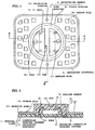
- an IC module has a terminal plate 1 in which connection terminal patterns 3 are arranged on one surface of an insulating substrate 2, an IC chip 4 arranged on the rear surface of the terminal plate 1 and sealed by the sealing member 5, and bonding wires 15 for electrically connecting pad portions of the IC chip 4 to the rear surfaces of the connection terminal patterns 3 through holes 16 of the insulating substrate 2.
- the reinforcing member 6 consists of a conductive material, and is integrally constituted by a ring portion 7 for covering the outer periphery of the sealing member 5 and a flange portion 8 for covering the insulating substrate 2.
- the shape of the outer periphery of the flange portion 8 has the same shape as that of the outer periphery of the terminal plate 1.
- the flange portion 8 is adhered to the insulating substrate 2 of the terminal plate 1 with an adhesive agent 13.
- the insulating substrate 2 has a through hole 10 at a position corresponding to a grounding connection terminal pattern 9.
- the reinforcing member 6 has a projection portion 11 projecting toward the insulating substrate 2. The projection portion 11 is fitted in the through hole 10 to position the reinforcing member 6.
- the reinforcing member 6 is electrically connected to the grounding connection terminal pattern 9 through the projection portions 11 and a conductive member 17 such as a conductive adhesive agent. In this manner, the IC is not damaged by electrostatic discharging from a capacitor formed by the terminal pattern 9 and the reinforcing member 6, and a shield effect can be expected.
- the ring portion 7 of the reinforcing member 6, as shown in FIG. 1 and FIG. 2, has a reinforcing rib 12 located above the IC chip 4 to improve the strength of the reinforcing member 6 and to protect the IC chip 4 from impacting external force.
- a plurality of window holes 14 constituting adhesive agent puddles. The adhesive agent 13 escapes from the window hole 14 to decrease the thickness of the adhesive agent layer, thereby improving the adhesive strength.
- the reinforcing member 6 according to this embodiment is obtained by forming the various holes and the outer shape by trimming after drawing of a metal plate, and is manufactured by press working using progressive dies. For this reason, the parts cost of the reinforcing member 6 is low.
- the IC module In mounting the IC module on a card base 18 for completing an IC card, as shown in FIG. 6, the IC module is engaged with a module mounting recessed portion 18a formed in the card base 18.
- the IC module is adhesively fixed to the recessed portion 18a of the card base 18 with an adhesive agent coated on the flange portion 8 of the reinforcing member 6.
- a thin adhesive agent layer is formed to improve the adhesive force.
- the reinforcing member 6 can also be manufactured by forging or casting. In this case, a reinforcing member 6 shown in FIG. 7 is obtained.
- the resistance of the IC module to external force can be improved, an accident that the IC module is damaged by disconnection of a bonding wire caused by peeling between an insulating substrate and a sealing member can be prevented, and a highly reliable IC card can be provided.
- the IC module can be fixedly mounted on the card base, the whole of the IC card can be made solid.
- the present invention in suitably used, as an IC card having a reinforced IC module mounted on the card, in various cards such as a cash card or a credit card.
Landscapes
- Engineering & Computer Science (AREA)
- Computer Hardware Design (AREA)
- Microelectronics & Electronic Packaging (AREA)
- Physics & Mathematics (AREA)
- General Physics & Mathematics (AREA)
- Theoretical Computer Science (AREA)
- Credit Cards Or The Like (AREA)
Applications Claiming Priority (3)
| Application Number | Priority Date | Filing Date | Title |
|---|---|---|---|
| JP28408797A JP3914620B2 (ja) | 1997-10-16 | 1997-10-16 | Icカード |
| JP28408797 | 1997-10-16 | ||
| PCT/JP1998/004668 WO1999021132A1 (fr) | 1997-10-16 | 1998-10-15 | Carte a circuit integre |
Publications (3)
| Publication Number | Publication Date |
|---|---|
| EP0952545A1 true EP0952545A1 (fr) | 1999-10-27 |
| EP0952545A4 EP0952545A4 (fr) | 2001-04-18 |
| EP0952545B1 EP0952545B1 (fr) | 2005-08-31 |
Family
ID=17674081
Family Applications (1)
| Application Number | Title | Priority Date | Filing Date |
|---|---|---|---|
| EP98947891A Expired - Lifetime EP0952545B1 (fr) | 1997-10-16 | 1998-10-15 | Carte a circuit integre |
Country Status (5)
| Country | Link |
|---|---|
| US (1) | US6166914A (fr) |
| EP (1) | EP0952545B1 (fr) |
| JP (1) | JP3914620B2 (fr) |
| DE (1) | DE69831394T2 (fr) |
| WO (1) | WO1999021132A1 (fr) |
Cited By (8)
| Publication number | Priority date | Publication date | Assignee | Title |
|---|---|---|---|---|
| WO2001027872A1 (fr) * | 1999-10-14 | 2001-04-19 | Gemplus | Renforcement d'un module de carte a puce |
| WO2003088139A1 (fr) * | 2002-04-18 | 2003-10-23 | Fci | Procede de conditionnement de microcircuits pour carte a puce et module ainsi obtenu |
| WO2003058713A3 (fr) * | 2002-01-08 | 2004-02-26 | Infineon Technologies Ag | Module a puce |
| WO2004102469A1 (fr) * | 2003-05-13 | 2004-11-25 | Nagraid Sa | Procédé d'assemblage d'un composant électronique sur un substrat |
| EP1519310A3 (fr) * | 2003-09-26 | 2005-07-06 | Kabushiki Kaisha Toshiba | Dispositif électronique portatif |
| EP2131312A4 (fr) * | 2007-03-23 | 2011-08-24 | Fujitsu Ltd | Dispositif électronique, équipement électronique dans lequel le dispositif électronique est conditionné, article sur lequel le dispositif électronique est monté et procédé de fabrication du dispositif électronique |
| EP2420960A1 (fr) * | 2010-08-17 | 2012-02-22 | Gemalto SA | Procédé de fabrication d'un dispositif électronique comportant un module indémontable et dispositif obtenu |
| EP2731058A1 (fr) * | 2012-11-13 | 2014-05-14 | Gemalto SA | Procédé de fabrication d'un module à puce électronique anti-charge électrostatique |
Families Citing this family (13)
| Publication number | Priority date | Publication date | Assignee | Title |
|---|---|---|---|---|
| SG80077A1 (en) * | 1998-10-19 | 2001-04-17 | Sony Corp | Semiconductor integrated circuit card manufacturing method, and semiconductor integrated circuit card |
| FR2806189B1 (fr) * | 2000-03-10 | 2002-05-31 | Schlumberger Systems & Service | Circuit integre renforce et procede de renforcement de circuits integres |
| US20050145609A1 (en) * | 2001-02-26 | 2005-07-07 | John Gregory | Method of forming an opening or cavity in a substrate for receiving an electronic component |
| JP4802398B2 (ja) * | 2001-06-08 | 2011-10-26 | 凸版印刷株式会社 | 非接触icカード |
| JP2003058853A (ja) * | 2001-08-17 | 2003-02-28 | Toppan Forms Co Ltd | 非接触型icカード及びその製造方法 |
| TWI299559B (en) * | 2002-06-19 | 2008-08-01 | Inpaq Technology Co Ltd | Ic substrate with over voltage protection function and method for manufacturing the same |
| TWI249232B (en) * | 2004-10-20 | 2006-02-11 | Siliconware Precision Industries Co Ltd | Heat dissipating package structure and method for fabricating the same |
| WO2007056503A2 (fr) * | 2005-11-08 | 2007-05-18 | Macsema, Inc. | Dispositifs d'informations |
| US7908118B2 (en) * | 2005-11-14 | 2011-03-15 | Macsema, Inc. | System and methods for testing, monitoring, and replacing equipment |
| US7680625B2 (en) * | 2005-11-14 | 2010-03-16 | Macsema, Inc. | Systems and methods for monitoring system performance |
| US20080106415A1 (en) * | 2006-11-08 | 2008-05-08 | Macsema, Inc. | Information tag |
| JP2013206122A (ja) * | 2012-03-28 | 2013-10-07 | Toppan Printing Co Ltd | Icモジュールとこれを搭載したicカード |
| EP3836010B1 (fr) * | 2019-12-12 | 2024-07-24 | Fingerprint Cards Anacatum IP AB | Module de capteur biométrique pour l'intégration dans une carte |
Family Cites Families (10)
| Publication number | Priority date | Publication date | Assignee | Title |
|---|---|---|---|---|
| JPS62201295A (ja) * | 1986-02-28 | 1987-09-04 | 松下電器産業株式会社 | Icカ−ドおよびその製造方法 |
| US4803546A (en) * | 1986-09-17 | 1989-02-07 | Fujitsu Limited | Heatsink package for flip-chip IC |
| JPS6440397A (en) * | 1987-08-07 | 1989-02-10 | Dainippon Printing Co Ltd | Portable electronic device |
| JPH01184193A (ja) * | 1988-01-19 | 1989-07-21 | Mitsubishi Electric Corp | 薄型半導体カード |
| EP0382203B1 (fr) * | 1989-02-10 | 1995-04-26 | Fujitsu Limited | Empaquetage céramique du type dispositif semi-conducteur et procédé pour son assemblage |
| JP2772739B2 (ja) * | 1991-06-20 | 1998-07-09 | いわき電子株式会社 | リードレスパッケージの外部電極構造及びその製造方法 |
| US5581445A (en) * | 1994-02-14 | 1996-12-03 | Us3, Inc. | Plastic integrated circuit card with reinforcement structure for protecting integrated circuit module |
| JPH08267973A (ja) * | 1995-03-30 | 1996-10-15 | Toppan Printing Co Ltd | Icカード |
| EP0766197A4 (fr) * | 1995-04-13 | 1999-12-29 | Dainippon Printing Co Ltd | Carte et module de circuit integre |
| DE19640466B4 (de) * | 1996-09-30 | 2006-06-14 | Robert Bosch Gmbh | Metallisches Trägerteil für elektronische Bauelemente oder Schaltungsträger und Verfahren zur Herstellung desselben |
-
1997
- 1997-10-16 JP JP28408797A patent/JP3914620B2/ja not_active Expired - Fee Related
-
1998
- 1998-10-15 DE DE69831394T patent/DE69831394T2/de not_active Expired - Fee Related
- 1998-10-15 US US09/308,382 patent/US6166914A/en not_active Expired - Fee Related
- 1998-10-15 WO PCT/JP1998/004668 patent/WO1999021132A1/fr not_active Ceased
- 1998-10-15 EP EP98947891A patent/EP0952545B1/fr not_active Expired - Lifetime
Cited By (16)
| Publication number | Priority date | Publication date | Assignee | Title |
|---|---|---|---|---|
| FR2799857A1 (fr) * | 1999-10-14 | 2001-04-20 | Gemplus Card Int | Procede pour le renforcement d'un module de circuit integre de carte a puce |
| WO2001027872A1 (fr) * | 1999-10-14 | 2001-04-19 | Gemplus | Renforcement d'un module de carte a puce |
| WO2003058713A3 (fr) * | 2002-01-08 | 2004-02-26 | Infineon Technologies Ag | Module a puce |
| CN100380638C (zh) * | 2002-01-08 | 2008-04-09 | 因芬尼昂技术股份公司 | 芯片模块 |
| DE10200382B4 (de) * | 2002-01-08 | 2006-05-04 | Infineon Technologies Ag | Chipmodul für Chipkarten |
| US7320738B2 (en) | 2002-04-18 | 2008-01-22 | Fci | Method for encapsulation of a chip card and module obtained thus |
| WO2003088139A1 (fr) * | 2002-04-18 | 2003-10-23 | Fci | Procede de conditionnement de microcircuits pour carte a puce et module ainsi obtenu |
| FR2838850A1 (fr) * | 2002-04-18 | 2003-10-24 | Framatome Connectors Int | Procede de conditionnement de microcircuits electroniques pour carte a puce et microcircuit electronique ainsi obtenu |
| WO2004102469A1 (fr) * | 2003-05-13 | 2004-11-25 | Nagraid Sa | Procédé d'assemblage d'un composant électronique sur un substrat |
| US7063267B2 (en) | 2003-09-26 | 2006-06-20 | Kabushiki Kaisha Toshiba | Portable electronic device |
| EP1519310A3 (fr) * | 2003-09-26 | 2005-07-06 | Kabushiki Kaisha Toshiba | Dispositif électronique portatif |
| EP2131312A4 (fr) * | 2007-03-23 | 2011-08-24 | Fujitsu Ltd | Dispositif électronique, équipement électronique dans lequel le dispositif électronique est conditionné, article sur lequel le dispositif électronique est monté et procédé de fabrication du dispositif électronique |
| EP2420960A1 (fr) * | 2010-08-17 | 2012-02-22 | Gemalto SA | Procédé de fabrication d'un dispositif électronique comportant un module indémontable et dispositif obtenu |
| WO2012022527A1 (fr) * | 2010-08-17 | 2012-02-23 | Gemalto Sa | Procédé de fabrication d'un dispositif électronique comportant un module indémontable et dispositif obtenu |
| EP2731058A1 (fr) * | 2012-11-13 | 2014-05-14 | Gemalto SA | Procédé de fabrication d'un module à puce électronique anti-charge électrostatique |
| WO2014075869A1 (fr) * | 2012-11-13 | 2014-05-22 | Gemalto Sa | Procede de fabrication d'un module a puce electronique anti-charge electrostatique |
Also Published As
| Publication number | Publication date |
|---|---|
| EP0952545A4 (fr) | 2001-04-18 |
| EP0952545B1 (fr) | 2005-08-31 |
| JPH11115356A (ja) | 1999-04-27 |
| US6166914A (en) | 2000-12-26 |
| JP3914620B2 (ja) | 2007-05-16 |
| DE69831394T2 (de) | 2006-06-01 |
| WO1999021132A1 (fr) | 1999-04-29 |
| DE69831394D1 (de) | 2005-10-06 |
Similar Documents
| Publication | Publication Date | Title |
|---|---|---|
| US6166914A (en) | IC card having a reinforcing member for reinforcing a sealing member | |
| US6346679B1 (en) | Substrate on which ball grid array type electrical part is mounted and method for mounting ball grid array type electrical part on substrate | |
| US9760754B2 (en) | Printed circuit board assembly forming enhanced fingerprint module | |
| EP0996962B1 (fr) | Dispositif a semi-conducteur et de type moule dans de la resine | |
| US20070069232A1 (en) | Semiconductor device with a resin-sealed optical semiconductor element | |
| TW317026B (fr) | ||
| KR19990044365A (ko) | 수지 밀봉형 반도체 장치 및 그 제조 방법 | |
| WO1999013516A1 (fr) | Montage muni d'un couvre-ouverture a moyens adhesifs de fermeture pour circuit integre optique a puces a bosses | |
| US20180108584A1 (en) | Semiconductor Substrate | |
| JP2844085B2 (ja) | 回路基板及び半導体素子の実装方法 | |
| KR19990022072A (ko) | 압력센서 및 압력센서의 제조방법 | |
| US8127997B2 (en) | Method for mounting an electronic component on a substrate | |
| EP1054346A2 (fr) | Carte à puce sans contact comprenant deux feuilles de revêtement | |
| US20140328032A1 (en) | Chip arrangement, chip card arrangement and method for manufacturing a chip arrangement | |
| US6046901A (en) | Support structure, electronic assembly | |
| US7915739B2 (en) | Method and arrangement for contact-connecting semiconductor chips on a metallic substrate | |
| US20070170564A1 (en) | Chip card module | |
| JP3358068B2 (ja) | Icカードおよびその製造方法 | |
| JPH11195101A (ja) | Icモジュールとそのモジュールを搭載したicカード | |
| JP2013225196A (ja) | 高信頼性接触型icカード | |
| JP2597139B2 (ja) | Icカード用icモジュール | |
| JPH04166396A (ja) | Icカードモジユール | |
| JPH0236309Y2 (fr) | ||
| JPH02235699A (ja) | Icカード | |
| JP2005332158A (ja) | Icモジュール及びicカード |
Legal Events
| Date | Code | Title | Description |
|---|---|---|---|
| PUAI | Public reference made under article 153(3) epc to a published international application that has entered the european phase |
Free format text: ORIGINAL CODE: 0009012 |
|
| 17P | Request for examination filed |
Effective date: 19990520 |
|
| AK | Designated contracting states |
Kind code of ref document: A1 Designated state(s): DE FR GB |
|
| A4 | Supplementary search report drawn up and despatched |
Effective date: 20010301 |
|
| AK | Designated contracting states |
Kind code of ref document: A4 Designated state(s): DE FR GB |
|
| RIC1 | Information provided on ipc code assigned before grant |
Free format text: 7G 06K 19/077 A |
|
| RAP1 | Party data changed (applicant data changed or rights of an application transferred) |
Owner name: CITIZEN WATCH CO. LTD. |
|
| 17Q | First examination report despatched |
Effective date: 20040331 |
|
| GRAP | Despatch of communication of intention to grant a patent |
Free format text: ORIGINAL CODE: EPIDOSNIGR1 |
|
| GRAS | Grant fee paid |
Free format text: ORIGINAL CODE: EPIDOSNIGR3 |
|
| GRAA | (expected) grant |
Free format text: ORIGINAL CODE: 0009210 |
|
| AK | Designated contracting states |
Kind code of ref document: B1 Designated state(s): DE FR GB |
|
| REG | Reference to a national code |
Ref country code: GB Ref legal event code: FG4D |
|
| PGFP | Annual fee paid to national office [announced via postgrant information from national office to epo] |
Ref country code: DE Payment date: 20050902 Year of fee payment: 8 |
|
| PGFP | Annual fee paid to national office [announced via postgrant information from national office to epo] |
Ref country code: FR Payment date: 20050929 Year of fee payment: 8 |
|
| REF | Corresponds to: |
Ref document number: 69831394 Country of ref document: DE Date of ref document: 20051006 Kind code of ref document: P |
|
| ET | Fr: translation filed | ||
| PLBE | No opposition filed within time limit |
Free format text: ORIGINAL CODE: 0009261 |
|
| STAA | Information on the status of an ep patent application or granted ep patent |
Free format text: STATUS: NO OPPOSITION FILED WITHIN TIME LIMIT |
|
| 26N | No opposition filed |
Effective date: 20060601 |
|
| PG25 | Lapsed in a contracting state [announced via postgrant information from national office to epo] |
Ref country code: DE Free format text: LAPSE BECAUSE OF NON-PAYMENT OF DUE FEES Effective date: 20070501 |
|
| GBPC | Gb: european patent ceased through non-payment of renewal fee |
Effective date: 20061015 |
|
| REG | Reference to a national code |
Ref country code: FR Ref legal event code: ST Effective date: 20070629 |
|
| PG25 | Lapsed in a contracting state [announced via postgrant information from national office to epo] |
Ref country code: GB Free format text: LAPSE BECAUSE OF NON-PAYMENT OF DUE FEES Effective date: 20061015 |
|
| PG25 | Lapsed in a contracting state [announced via postgrant information from national office to epo] |
Ref country code: FR Free format text: LAPSE BECAUSE OF NON-PAYMENT OF DUE FEES Effective date: 20061031 |
|
| PGFP | Annual fee paid to national office [announced via postgrant information from national office to epo] |
Ref country code: GB Payment date: 20060330 Year of fee payment: 8 |