EP0969370A2 - Rechnervorrichtung mit einem Cachespeicher und Ablaufverfolgungsfunktion - Google Patents
Rechnervorrichtung mit einem Cachespeicher und Ablaufverfolgungsfunktion Download PDFInfo
- Publication number
- EP0969370A2 EP0969370A2 EP99112981A EP99112981A EP0969370A2 EP 0969370 A2 EP0969370 A2 EP 0969370A2 EP 99112981 A EP99112981 A EP 99112981A EP 99112981 A EP99112981 A EP 99112981A EP 0969370 A2 EP0969370 A2 EP 0969370A2
- Authority
- EP
- European Patent Office
- Prior art keywords
- data
- pipe
- tracing
- stage
- line
- Prior art date
- Legal status (The legal status is an assumption and is not a legal conclusion. Google has not performed a legal analysis and makes no representation as to the accuracy of the status listed.)
- Withdrawn
Links
Images




Classifications
-
- G—PHYSICS
- G06—COMPUTING OR CALCULATING; COUNTING
- G06F—ELECTRIC DIGITAL DATA PROCESSING
- G06F11/00—Error detection; Error correction; Monitoring
- G06F11/36—Prevention of errors by analysis, debugging or testing of software
- G06F11/362—Debugging of software
- G06F11/3636—Debugging of software by tracing the execution of the program
- G06F11/364—Debugging of software by tracing the execution of the program tracing values on a bus
Definitions
- the present invention relates to a computer system and, more particularly, to a computer system having a cache memory and a data tracing function.
- a computer system generally includes a microprocessor (MPU), a ROM for storing a program for operating the MPU, a RAM for storing read/write data, and a peripheral device.
- MPU microprocessor
- ROM read/write data
- peripheral device a peripheral device for storing read/write data
- tracing circuit is generally provided to the MPU for examining whether or not the MPU operates expected functions, i.e., for debugging.
- the tracing circuit is connected to an external system bus such as an address bus or a data bus to obtain historical data of the MPU 21 at desired timing for storage thereof in the tracing memory.
- an external system bus such as an address bus or a data bus
- the tracing circuit connected to the external system bus cannot obtain the data accessed by the MPU when the accessed data is hit in the cache memory.
- the present invention provides a computer system including a pipe-line processor for pipe-line processing of an instruction code in synchrony with a pipe-line clock signal, a system memory for storing data for the pipe-Line processor, a system bus for transferring data between the pipe-line processor and the memory, a tracing circuit for storing trace data output from the pipe-line processor, and a trace data transfer circuit for transferring the trace data between the pipe-line processor and the tracing circuit independently of operation of the system bus.
- trace data can be supplied to the tracing circuit independently of the system bus without affecting the operation of the system bus and without losing real time processing by the pipe-line processor.
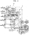
- a computer system includes a MPU 21 for executing signal processing based on a program, a peripheral device 17 such as a disk drive, a ROM 19 for storing the program, a RAM 20 for storing read/write data, a system bus 16 for transferring data between the MPU 21 and the external circuits including the peripheral device 17, the ROM 19 and the RAM 20, a tracing circuit 31 for tracing the signal processing executed by the MPU 21 together with read/write data, a tracing bus 10 for transferring the data and signals between the MPU 21 and the tracing circuit.
- the tracing circuit obtains the data from the MPU 21 for tracing the read/write data, address thereof and status signals.
- the MPU 21 includes a pipe-line processor 22, a data cache memory 23 for temporarily storing read/write data and an instruction cache memory 25 for storing instruction codes executed by the MPU 21.
- Each of the cache memories 23 and 25 includes a memory array and a cache controller not shown in the drawing.
- the pipe-line processor 22 functions for executing the instructions provided thereto at five separate stages.
- the MPU 21 includes stage blocks for executing five separate pipe-line stages including an instruction fetch stage (IF stage), a register fetch stage (RF stage), an execution stage (EX stage), a data fetch stage (DF stage) and a write back stage (WB stage).
- the MPU 21 also includes a pipe-line controller 37 for controlling the operation of the stage blocks, an external bus controller 48 for controlling the data transfer on the system bus 16 between the stage controllers 37 and the external circuits, and a data tracing bus controller 52 for controlling the data transfer on the tracing bus 10 between the MPU 21 and the tracing circuit 31.
- the IF stage block includes a program count generator 32, an instruction cache memory 25 and a program counter (PC) 34.
- the program counter 34 holds an instruction fetch address of the current instruction, and generates a next instruction fetch address for the next instruction by adding the current instruction fetch address and a specified value.
- An instruction code is fetched based on the address of the instruction cache memory 25 or the ROM 19 specified by the program counter 34, and stored in a RF stage register 73. After a branch instruction etc. is executed, the program count generator 32 generates an instruction fetch address for the branch instruction and stores the address thereof in the program counter 34.
- the RF stage block includes a pipe-line controller 37, a register file 38, and the RF stage register 73.
- the RF stage register 73 which is located adjacent the IF stage block, includes a PC latch 35 for latching an output from the program counter 34 and an instruction code latch 36 for latching an instruction code output from the instruction cache memory 25. These latches 35 and 36 in the RF stage register 73 operates for latching in synchrony with a pipe-Line clock signal PIPECLK.
- the pipe-line controller 37 operates for all the pipe-line stages, although it is shown in the RF stage block for convenience.
- the pipe-line controller 37 functions for reading an instruction code from the instruction code latch 36 for decoding the same to control overall operations in the pipe-line processing of the computer system.
- the pipe-line controller 37 outputs status signals STATUS#RF corresponding to the current instruction code, read/write signal R/W#RF and a memory request signal MRQ#RF.
- the symbol "xxx#RF" of the signal as used herein means that the signal is generated in a RF stage, and shifts to a symbol "xxx#EX" when the current stage shifts to an EX stage. That is, xxx#RF assumes a value same as the value of xxx#EX etc. and has a different effective timing therefrom.
- the register file 38 includes a plurality of registers numbered in sequence, and one of the registers is accessed for read/write thereof when the corresponding number is input as an access key.
- the register file 38 includes a decoder for a read/write address and each register includes a plurality of cascaded flip-flops.
- the data stored in the register of the register file 38 remains as it is when the data is read out simply by supplying the register number.
- the corresponding register number, write data and a clock signal for controlling the write operation are supplied.
- the EX stage block includes an arithmetic logic unit (ALU) 43 and an EX stage register 74.
- the EX stage register 74 includes three latches 40, 41 and 42 for latching ordinary process data output from the pipe-line controller 37 and the register file 38, and EX stage tracing latches 39 for latching status signals STATUS#RF and a read/write signal R/W#RF.
- the latches 40, 41 and 42 latch data output from the register file 38, the result of the calculation by the ALU 43 and the address of the read/write data, in synchrony with the pipe-line clock signal PIPECLK.
- the ALU 43 receives the instruction fetch address from the PC latch 35 through the latch 40 and outputs 38a and 38b from the register file 38 through the latch 41, then executes the arithmetic operation and supplies the result to the DF stage block.
- the DF stage block includes a data cache memory 23 and a DF stage register 75.
- the DF stage register 75 includes a DF stage tracing latch 46 for latching an output from the EX stage tracing latch 39, a latch 45 for latching an output from the ALU 43 and a latch 46 for latching the write data output from the latch 42.
- the data cache memory 23 transfers data between the same and the pipe-line processor 22 including the pipe-line controller 37, and stores read/write data. If requested data is not hit in the data cache memory 23, the data cache memory 23 delivers the address signal, the read/write signal and the status signal for the miss-hit data to the external bus controller 48, and requests the same to effect a read bus cycle therefor.
- the WB stage block includes a WB stage register 76 which includes a WB stage tracing latch 49 for latching an output from the DF stage tracing latch 44, a latch for latching an access address output from the latch 45, and a latch 51 for latching one of the read data output from the data cache memory 23 and the write data output from the latch 46 by using a selector.
- a WB stage register 76 which includes a WB stage tracing latch 49 for latching an output from the DF stage tracing latch 44, a latch for latching an access address output from the latch 45, and a latch 51 for latching one of the read data output from the data cache memory 23 and the write data output from the latch 46 by using a selector.
- the MPU 21 includes, in addition to the stage blocks as described above, the external bus controller 48 and the data tracing bus controller 52.
- the MPU 21 further includes address terminals 77 for an address S#ADDR, data terminals 78 for data S#DATA, a read/write signal terminal 79 for S#R/W, and status signal terminals 80 for status signals S#STATUS.
- the external bus controller 48 is connected to those terminals 77 to 80 as well as to the system bus 16 for transferring data through the system bus 16.
- the external bus controller 48 transfers data through the system bus 16 between the same and the external circuit such as ROM 19, RAM 20 or peripheral device 17, transfers a pre-fetch signal etc. between the instruction cache memory 25 and the ROM 19, transfers read data between the data cache memory 23 and the RAM 20, and receives write data from the WB stage block for storing the same to the RAM 20 by using a built-in write buffer 48a. That is, the external bus controller 48 outputs an address S#ADDR, a read/write signal S#R/W and status signals S#STATUS, while inputting/outputting a data S#DATA.
- the write operation to the memory, or RAM 20 is effected by the write buffer 48a without affecting and independently of the pipe-line processing of the computer system.
- the MPU 21 further includes, as trace data output terminals, address output terminals 63 for an address ADDR, data output terminals 64 for a data DATA, a read/write signal output terminal 65 for a read/write signal R/W, status signal output terminals 66 for status signals STATUS, a clock signal output terminal 67 for a clock signal CLK, and an enable signal output terminal 68 for an enable signal ENABLE.
- address output terminals 63 for an address ADDR data output terminals 64 for a data DATA
- a read/write signal output terminal 65 for a read/write signal R/W
- status signal output terminals 66 for status signals STATUS
- a clock signal output terminal 67 for a clock signal CLK
- an enable signal output terminal 68 for an enable signal ENABLE.
- the address output terminals 63 deliver the address ADDR of the data accessed by a load/store instruction
- the data output terminals 64 deliver the read/write data DATA
- the read/write signal output terminal 65 delivers a read/write signal for indicating whether the trace data is a read data or a write data.
- the status signal output terminals 66 deliver, in addition to the status information of the bus cycle, data size information as to whether the read/write data is a 1-byte (8-bit) data, 1-half-word (16-bit) data, 1-word (32-bit) data or a double-word (64-bit) data, effective data location information as to which bit is an effective data out of the 32-bit data when the data is a half-word data or a 1-word data and sequential information as to the order of the data.
- the data tracing bus controller 52 receives read/write data DATA accessed by the load/store instruction from the latch 51, an address ADDR from the latch 50, a read/write signal R/W and status signals STATUS from the latches 49, and delivers these data to the data tracing bus 10.
- the tracing circuit 31 is connected to the data tracing bus 10, and receives trace data therefrom through input terminals 69 to 72, 93 and 94.
- FIG. 3 there is shown the detail of a specific circuit portion of Fig. 2, generally designated by numeral 53, including the data tracing controller 52 and associated latches in the stage blocks.
- the latches 45, 46 and 51 in Fig. 3 are used for the tracing as well as for the pipe-line processing.
- the circuit portion 53 which implements a trace data transfer circuit together with the data tracing bus 10, includes cascaded tracing latches 39, 44 and 49 for transferring status signals STATUS#RF and a read/write signal R/W#RF from the pipe-line controller 37 through respective series of latches 39a, 44a and 49a and 39b, 44b and 49b to the final stage block, cascaded latches 45 and 50 for transferring the calculated address ADD from the ALU 43 to the final stage, cascaded latches 46 and 51 for transferring read/write data DATA to the final stage, and the data tracing bus controller 52.
- the data tracing bus controller 52 has an output terminal 67a for outputting a clock signal CLK, an output terminal 68a for outputting an enable signal ENABLE, output terminals 63a for outputting an address ADDR, output terminals 64a for outputting read/write data DATA, an output terminal 65a for outputting a read/write signal R/W, output terminals 66a for outputting status signals STSTUS, an output terminal 67a for outputting a clock signal CLK, and an output terminal 68a for outputting an enable signal ENABLE.
- the data tracing bus controller 52 passes trace data DATA and the clock signal CLK supplied from the final stage latches 49a, 49b, 50 and 51 to the output terminals 65a, 66a, 63a, 64a and 67a, respectively.
- the data tracing bus controller 52 includes an enable signal generator for generating an enable signal ENABLE and outputs the same through the output terminal 68a.
- the MPU 21 includes a pipe-line clock generator which generates a pipe-line clock signal PIPECLK and includes a two-input AND gate 54.
- the AND gate 54 receives the system clock signal CLK and inverted signal of the pipe-line mask signal PIPEMK and delivers an output to the latches 39a, 39b, 56, 44a, 44b, 57, 45, 46, 49a, 49b, 60, 50 and 51 at their clock inputs.
- the AND gate 54 passes the clock signal CLK as a pipe-line clock signal PIPECLK while the pipe-line mask signal assumes a low level, and stops the clock signal CLK to hold the PIPECLK signal at a low level while the pipe-line mask signal PIPEMK assumes a high level.
- the pipe-line clock signal controls signal processing in the pipe-line processing.
- the enable signal generator in the data tracing bus controller 52 includes a 2-input AND gate 55, and latches 56, 57 and 60.
- the latches 56 and 57 receive the pipe-line clock signal PIPECLK at their clock inputs, whereas the latch 56 receives a memory request signal MRQ#RF from the pipe-line controller 37 to deliver an output MRQ#EX to the latch 57, which delivers a memory request signal MRQ#DF.
- the AND gate 55 receives an inverted signal of the pipe-line mask signal PIPEMK and an output from the latch 57 to deliver an output to the data input of the latch 60.
- the memory request signal MRQ#RF is generated by the pipe-line controller 37 after the pipe-line controller 37 detects a load/store instruction.
- the memory request signal MRQ#RF assumes a high level or a low level depending on whether or not the external circuit such as RAM 20 or the peripheral device 17 is accessed for data transfer.
- the latch 60 receives the clock signal CLK at the clock input thereof, and delivers an enable signal ENABLE through the enable signal output terminal 68a.
- the enable signal ENABLE assumes a high level during a first clock period of the clock signal CLK after an instruction code accompanied by a load/ store instruction is received in the WB stage block, thereby rendering only the first clock pulse of the clock signal CLK to be effective. Thus, it is avoided to repeatedly store the same trace data in the tracing memory 58 when the pipe-line processing is stopped.
- the tracing circuit 31 includes a tracing memory 58 for storing trace data, an inverter 81, an increment circuit 59, a clock signal input terminal 67, an enable signal input terminal 68, address input terminals 69, read/write data input terminals 70, a read/write signal input terminal 71, and status signal input terminals 72.
- the tracing memory 58 includes a clock signal input MCLK, a write enable signal input MWE(-), address inputs MTA and data inputs MTD.
- the symbol "(-)" attached herein means that a negative logic scheme is used for the corresponding input.
- the tracing memory 58 receives data through the data input MTD at the address specified by the address signal supplied through the address inputs MTA, in synchrony with the clock signal CLK, when the signal MWE(-) is at a low level.
- the increment circuit (address adder) 59 includes a plurality of flip-flops 61, an adder 62 and a selector 82, and delivers an address (signal) TA to the address inputs MTA of the tracing memory 58 based on the clock signal CLK and the enable signal ENABLE received therein.
- the number of flip-flops 61 corresponds to the number of the address inputs of the tracing memory 58.
- the adder 62 increments (or decrements) the current address signal TA by one to calculate the address of the next trace data.
- the selector 82 selects an output from the flip-flop 61 when the enable signal ENABLE assumes a low level, and selects an output from the adder 62 when the enable signal ENABLE assumes a high level.
- the clock signal CLK rises to a next high level
- the selected output from the selector 82 is stored in the flip-flops 61.
- the increment circuit 59 delivers the same address. Accordingly, even after a plurality of clock pulses are supplied to the clock input MCLK of the tracing memory 58, the trace data is stored in the same address, thereby raising the efficiency of the tracing memory 58.
- the enable signal ENABLE input through the enable signal input terminal 68 is subjected to inversion by the inverter 81 to be input to the input MWE(-) of the tracing memory 58, thereby allowing the storage of the write data at a high level of the enable signal ENABLE.
- the trace data in the bus cycle specified by the load/store instruction among all the bus cycles is stored in the tracing memory 58.
- the data signals TD input to the tracing circuit 31 include address ADD, data DATA, read/write signal R/W and status signal STATUS, which are supplied to the inputs MTD of the tracing memory 58 and received therein at the timing of a low level of the write enable signal WE(-).
- the data width or number of the inputs TD of the tracing memory 58 corresponds to the sum of the data widths of these data.
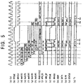
- FIG. 5 there is shown a specific example wherein five instructions Inst1 to Inst 5 are delivered from the MPU, wherein (N) attached to Inst1 indicates that Inst1 is a normal instruction which stays within the MPU 21 and does not involve a read/write operation for the external circuit, (R) attached to Inst2 and Inst4 indicates that Inst2 and inst4 are read instructions, and (W) attached to Inst3 and Inst5 indicates that Inst3 and Inst5 are write instructions.
- "IC Hit” attached to each instruction indicates that the instruction cache memory 25 is hit in the instruction and
- “DC Hit” attached to specific instructions indicates that the data cache memory 23 is hit in the specific instruction, whereas "DC Miss” indicates that the data cache memory 23 is miss hit.
- the memory request signal MRQ#RF delivered from the pipe-line controller 37 is latched by the EX stage tracing latch 56 at the next rise of the pipe-line clock signal PIPECLK, whereby the latch 56 delivers a MRQ#EX signal.
- MRQ#EX signal assumes a high level when a load/store instruction accompanied by a data access for read/write is executed. For example, when Inst2(R) is decoded at the RF stage and detected to be an instruction accompanied by a read operation, the pipe-line controller 37 delivers a high level for MRQ#RF to the latch 56 at time t2. When the pipe-line clock signal PIPECLK rises at time t3, the latch latches the high level for MRQ#RF to raise an output MRQ#EX from the latch 56, as shown at row (j) of Fig. 5.
- MQR#EX signal in the fifth instruction Inst5(W) is latched at time t6 by the latch 56 until the EX stage for Inst5 is finished at time t10. If a succeeding instruction Inst6 not shown is a normal instruction, the output of the pipe-line controller 37 assumes a low level at time t6, which is latched by the latch 56 at time t11 at a rising edge of the pipe-line clock signal, thereby lowering the output of the latch 56 to a low level.
- the latch 57 latches the output of the latch 56 at a rising edge of the pipe-line clock signal. That is, MRQ#DF signal is obtained by latching an output MRQ#EX from the latch 56 at a rising edge of the pipe-line clock signal PIPECLK, and thus is shifted from MRQ#EX by one clock of the pipe-line clock signal.
- the latch 60 latches an output from the AND gate 55 at a rising edge of the clock signal CLK and delivers an output as an enable signal ENABLE, as shown at row (k) of Fig. 5.
- the AND gate 55 receives MRQ#DF signal and an inversion of pipe-line mask signal PIPEMK to deliver a MRQ#DF signal only when the pipe-line mask signal PIPEMK assumes a low level.
- the latch 60 latches an output from the AND gate 55 at a rising edge of the clock signal CLK to deliver an enable signal ENABLE.
- the enable signal ENABLE assumes a high level at a first clock pulse of the clock signal CLK after an instruction accompanied by a load/store instruction reaches to the WB stage block.
- MRQ#DF signal in Inst2(R) assumes a high level at time t4, which makes the output of the AND gate 55 at a high level due to a low level of the pipe-line mask signal at this stage.
- the enable signal ENABLE output from the AND gate 55 assumes a high level as shown at row (1) of Fig. 5.
- the MRQ#DF signal of Inst4(R) assumes a high level at time t6, which makes the output of the AND gate 55 at a high level due to a low level of the pipe-line mask signal PIPEMK at this stage.
- the pipe-line mask signal PIPEMK signal rises at the last half of time t6, to lower the output of the AND gate 55.
- the latch 60 after latching the output of the AND gate 55 at a rising edge of the clock signal CLK, delivers a low level for the enable signal ENABLE at time t7, as shown at row (1) of fig. 5.
- FIGs. 6 and 7 there is shown processing for instructions Inst3(W) and Inst2(R), respectively, wherein a square shows a timing of generation of the corresponding signal, a circle shows a timing of transferring of the signal to the tracing bus, and a dot shows a shift of the signal to a next stage.
- the instruction code for Inst3(W) is fetched at t2 during the IF stage and decoded at t3 during the RF stage.
- the pipe-line controller 37 reads the write data from the register in the register file 38 specified by the instruction and stores the same in the latch 42, and at the same time t3, delivers a read/write signal R/W#RF and status signals STATUS#RF thereof to the latches 39a and 39b.
- the write data, read/write signal and the statue signal are latched at time t4 by the latches 42, 39a and 39b, respectively, at a rising edge of the pipe-line clock signal PIPECLK, and delivered as Write Data#EX, R/W#EX and STATUS#EX, respectively, to the next EX stage.
- the ALU 43 then calculates the address for the write data and delivers the address to the latch 45 at time t4 during the EX stage.
- the address ADDR and the data DATA are stored in the data cache memory 23.
- the write data is stored in the write buffer 48a provided in the external bus controller 48, and also stored in the RAM 20 by the external bus controller 48 when the system bus 16 is not used for other task.
- these signals ADDR, DATA, R/W and STATUS are supplied to the tracing circuit through the tracing bus 10, and stored in the address 1H of the tracing memory 58 (refer to (g) of Fig. 5).
- the instruction Inst2(R) is fetched at time t1 during the IF stage, and decoded at time t2 during the RF stage.
- the pipe-line controller 37 delivers a read/write signal R/W#RF indicating a read instruction and status signals STATUS#RF thereof at time t2.
- the signals R/W#RF and STATUS#RF are latched by the latches 42, 39a and 39b at a rising edge of the pipe-line clock signal at time t3 during the EX stage, and delivered as signals R/W#EX and STATUS#EX.
- the ALU 43 calculates the address for the write data at time t3 during the EX stage and delivers the same to the latch 45.
- the address, read/write signal and the status signal are latched by the latches 45, 44a and 44b, respectively, which deliver signals Address#DF, R/W#DF and STATUS#DF.
- the address is also supplied to the data cache memory 23. If the data is hit in the data cache memory 23, the data cache memory 23 reads data therein based on the supplied address and delivers the read data to the latch 51 through the selector 91.
- the selector 91 selects the write data when the read/write signal indicates a write mode and selects the read data when the read/write signal indicates a read mode.
- the address ADDR and the data DATA are read from the data cache memory 23.
- the data cache memory 23 is miss hit, as in the case of Inst4 of Fig. 5, a read bus cycle is requested of the external bus controller 48, the pipe-line clock signal is maintained at a high level to stop the pipe-line processing, and the data is read from the RAM 20.
- the address, the read data, the read/write signal and the status signal are latched by the latches 50, 51, 49a and 49b, which deliver Address#WB, Read Data#WB, R/W#WB and STATUS#WB, respectively.
- These signals area also supplied to the tracing circuit 31 through the tracing bus 10, and stored in the address 0H in the tracing memory 58 (refer to (g) of Fig. 5).
- the trace data in a single instruction are generated in the different stages depending on the signals.
- the effective timing of the data depends on the storage instruction or the load instruction.
- these different timing is adjusted by the number of stages of cascaded latches provided from the stage block at which the signal is generated to the stage block at which the signal is transferred to the tracing circuit, the latches operating in synchrony with the pipe-line clock signal.
- the tracing circuit can receive the signals at a uniform timing for any instructions.
- the timing does not change even if the instruction concerns storage or load of data or if the read data is hit or miss hit in the cache memory.
- the inversion of the order of the trace data, wherein the succeeding data is traced before the preceding data, as encountered in the conventional device does not arise, whereby the data tracing can be effected in the order without using a monitor circuit for the bus cycle.
- the computer system generally operates by transferring data between the MPU 21 and the external circuit such as the peripheral device 17, RAM 20 and the ROM 19, as mentioned before.
- the pipe-line processing is executed in a single stage cycle with the case of hit or miss hit in the cache memories, wherein the computers system executes a single instruction in a single pipe-line cycle.
- the pipe-line processing for the instruction such as Inst1 to Inst5 is executed in a single instruction cycle including five separate stages by passing one stage by one stage. If the cache memory is miss hit, the pipe-line controller 37 delivers a low level for the pipe-line clock signal to stop the operation of all the stages for the instruction.
- the pipe-line mask signal PIPEMK is inactivated to activate the pipe-line clock signal PIPECLK, whereby the instruction advances in synchrony with the pipe-line clock signal.
- the program count generator 32 updates the count in the program counter 34, which delivers a PC address to the instruction cache memory 25.
- the PC address is also stored in the PC latch 35 in the RF stage register73.
- the instruction code is read from the instruction cache memory 25 based on the PC address and stored in the instruction code latch 36 in the RF stage register 73
- the fetch address and a request for the fetch bus cycle are delivered from the instruction cache memory 25 to the external bus controller 48.
- the external bus controller 48 upon miss hit of instruction code, receives the fetch address from the instruction cache memory 25 to access the ROM 19.
- the external bus controller 48 upon miss hit of data, receives the access address, which is obtained by calculation and stored in the latch 45 during the EX stage, through the data cache memory 23 to access the RAM 20 through the system bus 16.
- the data stored in the register in the register file 38 is read as outputs 38a and 38b based on the signals from the pipe-line controller 37.
- the register number and the PC address from the program counter 34 are latched by latches 40, 41 and 42 in the EX stage register 74.
- the ALU 43 calculates based on the data read from the latches 40 and 41 in the EX stage register 74. At this stage, if the instruction code indicates a load/store instruction, the result of the calculation indicates the address of the data. The output of the ALU 43 is supplied to the Latches 45 and 46 and stored therein.
- the MPU 21 accesses the data cache memory 23 based on the address obtained during the EX stage, if the instruction indicates a load/store instruction. If the data cache memory 23 is hit, as shown by "DC Hit" in Fig. 5 for Inst2(R) etc., the data is read from the data cache memory 23 when the instruction code indicates a load instruction, and is stored in the data cache memory 23 during the WB stage. The data is also stored in the latch 51 in the WB stage register 76. If the data is miss hit, the MPU 21 accesses the peripheral device or the RAM 20 through the external bus controller 48 and the system bus 16.
- the read data read from the latch 51 in the WB stage register 76 is stored again to the register file 38.
- the data latched by the latch 51, the read/write signal and the status signal read from the latch 50 are supplied to the data tracing bus controller 52.
- the memory request signal MRQ#DF becomes active and thus the memory request signal MRQ#DF is generated after a single clock cycle, as a result of which the write enable signal assumes a high level to output the trace data in the final WB stage after all the trace data are prepared in the WB stage block.
- the data tracing bus controller 52 stores the trace data including the address, data, read/write signal and the status signal in synchrony with the pipe-line clock signal, and supplies these data to the data tracing bus 10 through the tracing terminals 63 to 66.
- the first instruction Inst1(N) is executed in the first through fifth stages thereof, which does not involve trace data because the instruction is a normal instruction without a load/store operation.
- the pipe-line controller 37 supplies the PC address in the program counter 34 to the instruction cache memory 25, fetches instruction Inst2 from the cache memory 25, and allows the latch 36 to latch the fetched instruction.
- the pipe-line controller 37 decodes Isnt2 by reference to the data in the instruction code latch 36, and allows the latches 40 and 41 to latch the address of the RAM 20 to be accessed.
- the pipe-line controller 37 also delivers a MRQ#RF signal, a R/W#RF signal, a STATUS#RF signal, to store these signals in the tracing latches 39 in synchrony with the pipe-line clock signal.
- the ALU 43 calculates based on the data stored in the latches 40 and 41, and stores the result of the calculation, i.e., address B01, in the latch 45.
- the outputs from the tracing latches 89 including MRQ#EX, R/W#EX and STATUS#EX signals are latched by the tracing latches 44 in synchrony with the pipe-line clock signal. As a result, the MRQ#EX signal rises to a high level as shown in (j) of Fig. 5.
- the address B01 and the read signal stored in the latch 45 are supplied to the data cache memory 23. If the access address B01 is hit in the data cache memory 23, the data cache memory 23 delivers data D01 to the latch 51 through the selector 91. The access address B01 and the read data D01 are then latched by the latches 50 and 51, respectively, in synchrony with a next pulse of the pipe-line clock signal.
- the read/write signal R/W and the status signal STATUS output from the tracing latch 44 are latched by the latch 49 in synchrony with the pipe-line clock signal.
- the MRQ#EX signal is latched by the tracing latch 44, the output of which is a MRQ#DE signal and assumes a high level (refer to (k) of Fig. 5).
- the MRQ#DF signal is supplied together with an inverted signal of the pipe-line clock signal to the AND gate 55, which delivers an enable signal ENABLE#DF.
- the ENABLE#DF signal is latched by the tracing latch 60 in synchrony with the clock signal CLK.
- the pipe-line controller 37 writes the data stored in the latch 51 to one of the registers in the register file 38.
- the latches 50 and 51 deliver the address and the data to the address output terminals 63a and the data output terminals 64a, respectively (refer to (m) and (n) of Fig. 5).
- the read/write signal R/W#DF and the status signal STATUS#DF output from the tracing latch 49 are delivered to the output terminals 65a and 66a, respectively (refer to (o) and (p) of Fig. 5.
- the enable signal ENABLE output from the tracing latch 49 is delivered to the output terminal 68a in synchrony with the clock signal CLK. Thus, the enable signal assumes a high level at time t5 (refer to (1) of Fig. 5.
- data in the instruction can be also traced by the tracing circuit 31.
- the tracing terminals 63a to 68a dedicated for the tracing can receive the trace data through the dedicated tracing bus 10.
- the tracing circuit 31 stores these trace data in the tracing memory 58 at the address 0H. After the trace data are stored in the tracing memory 58, the address is incremented by one to assume 1H and prepared to a next write operation.
- instruction Inst3 indicates a write instruction of data D02 at the address of B02 in the RAM 20
- the operations from time t2 to time t5 are similar to the conventional process.
- the processing for the status signal, the read/write signal and the memory request signal are similar to those in the instruction Inst2.
- the address B02 and the data D0 stored in the latches 50 and 51 are delivered to the data cache memory 23 and stored therein.
- the trace data is supplied to the tracing circuit 31 through the tracing bus 10, and stored in the tracing memory 58 at the address of 1H (refer to (g) of Fig. 5).
- the address is incremented by one in synchrony with the clock signal CLK to assume 2H to prepare a next write operation.
- the data cache memory 23 also requests the pipe-line controller 37 to stop the pipe-line processing.
- the pipe-line controller 37 responds to the request and maintains the pipe-line mask signal PIPEMK at a high level between time t6 and time t10, which in turn maintains the pipe-line clock signal at a low level.
- all the stage blocks stop their pipe-line processing of the instruction (refer to (c) of Fig. 5).
- the shift of the status signal, read/write signal and the memory request signal is also stopped, whereby the latches maintains their states.
- the external bus controller 48 executes a read bus cycle for the instruction Inst4, and reads the data D03.
- the data cache memory 23 allows the latch 51 to latch the data D03 through the selector 91 and requests the pipe-line controller 37 to cancel the stop of pipe-line processing.
- the pipe-line controller 37 then lowers the pipe-line mask signal to a low level (refer to (c) of Fig. 5), activates the pipe-line clock signal to allow the stage blocks to operate for the pipe-line processing.
- the data stored in the latch 51 is supplied to and stored in a specified register in the register file 38.
- the trace data including the address B03 and the read data D03 are also supplied to the tracing circuit 31 through the tracing bus 10.
- the tracing circuit 31 receives these trace data and stores the same in the tracing memory 58 at an address 2H (refer to (q) of Fig. 5). After the storage of the trace data, the address of the tracing memory is incremented by one to prepare a next write operation.
- the operations from time t4 to time t11 are similar to those for the instruction Inst3.
- the pipe-line controller 37 writes the data (address B04 and data D04) stored in the latches 50 and 51 to the data cache memory 23, as well as to the write buffer 48a in the external bus controller 48.
- the pipe-line processing of the MPU for the instruction Inst5 is finished.
- the trace data for the instruction Inst5 are supplied to the tracing circuit 31 through the tracing bus 10, which stores these data in the tracing memory 58 at the address 3H.
- the address of the tracing memory 58 is then incremented by one to prepare a next write operation.
- a dedicated tracing bus is provided for the tracing circuit. Also, all the trace data are prepared for tracing at the final stage of the pipe-line processing cycle. Thus, the tracing can be conducted without losing real time processing and maintaining the data cache function of the computer system. Further, the tracing operation does not affect the operation of the pipe-line processing by the computer system.
Landscapes
- Engineering & Computer Science (AREA)
- Theoretical Computer Science (AREA)
- Computer Hardware Design (AREA)
- Quality & Reliability (AREA)
- Physics & Mathematics (AREA)
- General Engineering & Computer Science (AREA)
- General Physics & Mathematics (AREA)
- Debugging And Monitoring (AREA)
- Advance Control (AREA)
- Memory System Of A Hierarchy Structure (AREA)
Applications Claiming Priority (2)
| Application Number | Priority Date | Filing Date | Title |
|---|---|---|---|
| JP18891598A JP3214613B2 (ja) | 1998-07-03 | 1998-07-03 | マイクロプロセッサ及びデータ処理システム |
| JP18891598 | 1998-07-03 |
Publications (2)
| Publication Number | Publication Date |
|---|---|
| EP0969370A2 true EP0969370A2 (de) | 2000-01-05 |
| EP0969370A3 EP0969370A3 (de) | 2004-08-18 |
Family
ID=16232119
Family Applications (1)
| Application Number | Title | Priority Date | Filing Date |
|---|---|---|---|
| EP99112981A Withdrawn EP0969370A3 (de) | 1998-07-03 | 1999-07-05 | Rechnervorrichtung mit einem Cachespeicher und Ablaufverfolgungsfunktion |
Country Status (3)
| Country | Link |
|---|---|
| US (1) | US6453410B1 (de) |
| EP (1) | EP0969370A3 (de) |
| JP (1) | JP3214613B2 (de) |
Cited By (1)
| Publication number | Priority date | Publication date | Assignee | Title |
|---|---|---|---|---|
| WO2009015225A1 (en) * | 2007-07-24 | 2009-01-29 | Qualcomm Incorporated | Data access tool for programmable graphics hardware |
Families Citing this family (4)
| Publication number | Priority date | Publication date | Assignee | Title |
|---|---|---|---|---|
| GB2362729B (en) * | 1999-12-23 | 2004-02-11 | St Microelectronics Sa | Memory access debug facility |
| US7149926B2 (en) * | 2003-05-22 | 2006-12-12 | Infineon Technologies Ag | Configurable real-time trace port for embedded processors |
| JP4608276B2 (ja) | 2004-10-04 | 2011-01-12 | ルネサスエレクトロニクス株式会社 | トレース制御回路、マイクロプロセッサ及びトレース制御方法 |
| WO2011065354A1 (ja) | 2009-11-26 | 2011-06-03 | 日本電気株式会社 | バスモニタ回路及びバスモニタ方法 |
Family Cites Families (20)
| Publication number | Priority date | Publication date | Assignee | Title |
|---|---|---|---|---|
| US4674089A (en) * | 1985-04-16 | 1987-06-16 | Intel Corporation | In-circuit emulator |
| JPH0731615B2 (ja) * | 1986-04-18 | 1995-04-10 | 日本電気株式会社 | 情報処理装置 |
| JPS6383841A (ja) | 1986-09-29 | 1988-04-14 | Hitachi Ltd | プログラムテスト可能な計算機中央処理装置 |
| JPH0251745A (ja) | 1988-08-15 | 1990-02-21 | Fujitsu Ltd | ヒストリデータ制御方式 |
| JPH03137736A (ja) | 1989-10-24 | 1991-06-12 | Fujitsu Ltd | マイクロプロセッサ動作トレース方式 |
| JPH03256141A (ja) | 1990-03-07 | 1991-11-14 | Fujitsu Ltd | 実行確認方式 |
| JPH03263136A (ja) | 1990-03-13 | 1991-11-22 | Nec Corp | パイプラインのトレース方式 |
| JPH04296944A (ja) | 1991-03-04 | 1992-10-21 | Mitsubishi Electric Corp | マイクロプロセッサ |
| JPH0683705A (ja) | 1992-09-03 | 1994-03-25 | Nec Ic Microcomput Syst Ltd | マイクロコンピュータlsi |
| JPH06161818A (ja) | 1992-10-14 | 1994-06-10 | Nec Corp | 一次キャッシュメモリ内蔵マイクロプロセッサの命令トレース制御方式 |
| JPH06161822A (ja) * | 1992-11-20 | 1994-06-10 | Mitsubishi Electric Corp | マイクロプロセッサ |
| US5564028A (en) * | 1994-01-11 | 1996-10-08 | Texas Instruments Incorporated | Pipelined data processing including instruction trace |
| JPH07271705A (ja) | 1994-02-09 | 1995-10-20 | Hitachi Ltd | データプロセッサ及びこれを用いたトレース回路 |
| JPH08171505A (ja) | 1994-12-16 | 1996-07-02 | Fujitsu Ltd | 半導体装置 |
| JPH08335177A (ja) | 1995-06-07 | 1996-12-17 | Oki Electric Ind Co Ltd | プロセッサ動作観察方法及び装置 |
| JP3443720B2 (ja) * | 1995-12-12 | 2003-09-08 | 株式会社日立製作所 | エミュレータ |
| JP2872117B2 (ja) | 1996-06-27 | 1999-03-17 | 日本電気アイシーマイコンシステム株式会社 | マイクロプロセッサ |
| US5751735A (en) * | 1996-11-14 | 1998-05-12 | Hewlett-Packard Company | Integrated debug trigger method and apparatus for an integrated circuit |
| JP3349911B2 (ja) | 1997-02-28 | 2002-11-25 | エヌイーシーマイクロシステム株式会社 | マイクロプロセッサ及びその開発支援装置 |
| US5933626A (en) * | 1997-06-12 | 1999-08-03 | Advanced Micro Devices, Inc. | Apparatus and method for tracing microprocessor instructions |
-
1998
- 1998-07-03 JP JP18891598A patent/JP3214613B2/ja not_active Expired - Fee Related
-
1999
- 1999-07-05 EP EP99112981A patent/EP0969370A3/de not_active Withdrawn
- 1999-07-06 US US09/348,042 patent/US6453410B1/en not_active Expired - Lifetime
Cited By (2)
| Publication number | Priority date | Publication date | Assignee | Title |
|---|---|---|---|---|
| WO2009015225A1 (en) * | 2007-07-24 | 2009-01-29 | Qualcomm Incorporated | Data access tool for programmable graphics hardware |
| US8760457B2 (en) | 2007-07-24 | 2014-06-24 | Qualcomm Incorporated | Data access tool for programmable graphics hardware |
Also Published As
| Publication number | Publication date |
|---|---|
| JP3214613B2 (ja) | 2001-10-02 |
| US6453410B1 (en) | 2002-09-17 |
| EP0969370A3 (de) | 2004-08-18 |
| JP2000020345A (ja) | 2000-01-21 |
Similar Documents
| Publication | Publication Date | Title |
|---|---|---|
| TWI476597B (zh) | 資料處理裝置及半導體積體電路裝置 | |
| US5652900A (en) | Data processor having 2n bits width data bus for context switching function | |
| US4037213A (en) | Data processor using a four section instruction format for control of multi-operation functions by a single instruction | |
| US5381360A (en) | Modulo arithmetic addressing circuit | |
| JPH04313121A (ja) | インストラクションメモリ装置 | |
| KR100303712B1 (ko) | 파이프라인기계에서의어드레스파이프라인을위한방법및장치 | |
| KR100351527B1 (ko) | 코드브레이크포인트디코더 | |
| EP0969370A2 (de) | Rechnervorrichtung mit einem Cachespeicher und Ablaufverfolgungsfunktion | |
| US5742842A (en) | Data processing apparatus for executing a vector operation under control of a master processor | |
| US4896264A (en) | Microprocess with selective cache memory | |
| US5276822A (en) | System with enhanced execution of address-conflicting instructions using immediate data latch for holding immediate data of a preceding instruction | |
| KR920002573B1 (ko) | 데이타 처리기 | |
| KR920001102B1 (ko) | 정보 처리 장치 | |
| JPS6079431A (ja) | プログラマブルコントローラのパイプライン処理方法 | |
| JP2872117B2 (ja) | マイクロプロセッサ | |
| KR100246465B1 (ko) | 마이크로프로세서 스택 명령어의 수행사이클을 줄이기 위한 장치 및 그 방법 | |
| JP3441847B2 (ja) | データメモリを有するプロセッサ | |
| JPH0385636A (ja) | 命令先行制御装置 | |
| JPH0683986A (ja) | シングルチップ・マイクロコンピュータ | |
| JP3366235B2 (ja) | データ読み出し制御装置 | |
| JP3693873B2 (ja) | マスクビット数演算装置、ベクトル処理装置、情報処理装置 | |
| JP2696578B2 (ja) | データ処理装置 | |
| JPH0512009A (ja) | デイジタル信号処理装置 | |
| JPH033047A (ja) | 演算機能付きメモリ | |
| JPH09128235A (ja) | 5段パイプライン構造のプログラマブルコントローラ |
Legal Events
| Date | Code | Title | Description |
|---|---|---|---|
| PUAI | Public reference made under article 153(3) epc to a published international application that has entered the european phase |
Free format text: ORIGINAL CODE: 0009012 |
|
| AK | Designated contracting states |
Kind code of ref document: A2 Designated state(s): AT BE CH CY DE DK ES FI FR GB GR IE IT LI LU MC NL PT SE |
|
| AX | Request for extension of the european patent |
Free format text: AL;LT;LV;MK;RO;SI |
|
| RAP1 | Party data changed (applicant data changed or rights of an application transferred) |
Owner name: NEC ELECTRONICS CORPORATION |
|
| PUAL | Search report despatched |
Free format text: ORIGINAL CODE: 0009013 |
|
| AK | Designated contracting states |
Kind code of ref document: A3 Designated state(s): AT BE CH CY DE DK ES FI FR GB GR IE IT LI LU MC NL PT SE |
|
| AX | Request for extension of the european patent |
Extension state: AL LT LV MK RO SI |
|
| 17P | Request for examination filed |
Effective date: 20050211 |
|
| 17Q | First examination report despatched |
Effective date: 20050315 |
|
| AKX | Designation fees paid |
Designated state(s): DE GB |
|
| RBV | Designated contracting states (corrected) |
Designated state(s): DE GB |
|
| STAA | Information on the status of an ep patent application or granted ep patent |
Free format text: STATUS: THE APPLICATION IS DEEMED TO BE WITHDRAWN |
|
| 18D | Application deemed to be withdrawn |
Effective date: 20050726 |