EP0969507A1 - EEPROM-Speicherzelle und deren Herstellungsverfahren - Google Patents
EEPROM-Speicherzelle und deren Herstellungsverfahren Download PDFInfo
- Publication number
- EP0969507A1 EP0969507A1 EP98830390A EP98830390A EP0969507A1 EP 0969507 A1 EP0969507 A1 EP 0969507A1 EP 98830390 A EP98830390 A EP 98830390A EP 98830390 A EP98830390 A EP 98830390A EP 0969507 A1 EP0969507 A1 EP 0969507A1
- Authority
- EP
- European Patent Office
- Prior art keywords
- region
- substrate
- source region
- heavily doped
- drain region
- Prior art date
- Legal status (The legal status is an assumption and is not a legal conclusion. Google has not performed a legal analysis and makes no representation as to the accuracy of the status listed.)
- Granted
Links
- 238000004519 manufacturing process Methods 0.000 title description 7
- 239000000758 substrate Substances 0.000 claims abstract description 41
- 239000004065 semiconductor Substances 0.000 claims abstract description 6
- 238000000034 method Methods 0.000 claims description 18
- 229910021332 silicide Inorganic materials 0.000 claims description 17
- FVBUAEGBCNSCDD-UHFFFAOYSA-N silicide(4-) Chemical compound [Si-4] FVBUAEGBCNSCDD-UHFFFAOYSA-N 0.000 claims description 16
- 239000002019 doping agent Substances 0.000 claims description 7
- 238000002513 implantation Methods 0.000 claims description 7
- 206010010144 Completed suicide Diseases 0.000 claims description 4
- 239000011159 matrix material Substances 0.000 claims description 4
- 239000010410 layer Substances 0.000 description 46
- 229910021420 polycrystalline silicon Inorganic materials 0.000 description 13
- 229920005591 polysilicon Polymers 0.000 description 13
- 239000007943 implant Substances 0.000 description 9
- 230000015572 biosynthetic process Effects 0.000 description 4
- 229910052723 transition metal Inorganic materials 0.000 description 4
- 150000003624 transition metals Chemical class 0.000 description 4
- 125000006850 spacer group Chemical group 0.000 description 3
- 239000003989 dielectric material Substances 0.000 description 2
- RTAQQCXQSZGOHL-UHFFFAOYSA-N Titanium Chemical compound [Ti] RTAQQCXQSZGOHL-UHFFFAOYSA-N 0.000 description 1
- 239000002131 composite material Substances 0.000 description 1
- 238000000151 deposition Methods 0.000 description 1
- 238000005530 etching Methods 0.000 description 1
- 238000009413 insulation Methods 0.000 description 1
- 238000012216 screening Methods 0.000 description 1
- 229910052710 silicon Inorganic materials 0.000 description 1
- 239000010703 silicon Substances 0.000 description 1
- 239000002344 surface layer Substances 0.000 description 1
- 239000010936 titanium Substances 0.000 description 1
- 229910052719 titanium Inorganic materials 0.000 description 1
- -1 titanium or tungsten Chemical class 0.000 description 1
- WFKWXMTUELFFGS-UHFFFAOYSA-N tungsten Chemical compound [W] WFKWXMTUELFFGS-UHFFFAOYSA-N 0.000 description 1
- 229910052721 tungsten Inorganic materials 0.000 description 1
- 239000010937 tungsten Substances 0.000 description 1
Images


Classifications
-
- H—ELECTRICITY
- H10—SEMICONDUCTOR DEVICES; ELECTRIC SOLID-STATE DEVICES NOT OTHERWISE PROVIDED FOR
- H10B—ELECTRONIC MEMORY DEVICES
- H10B41/00—Electrically erasable-and-programmable ROM [EEPROM] devices comprising floating gates
- H10B41/30—Electrically erasable-and-programmable ROM [EEPROM] devices comprising floating gates characterised by the memory core region
- H10B41/35—Electrically erasable-and-programmable ROM [EEPROM] devices comprising floating gates characterised by the memory core region with a cell select transistor, e.g. NAND
-
- H—ELECTRICITY
- H10—SEMICONDUCTOR DEVICES; ELECTRIC SOLID-STATE DEVICES NOT OTHERWISE PROVIDED FOR
- H10B—ELECTRONIC MEMORY DEVICES
- H10B69/00—Erasable-and-programmable ROM [EPROM] devices not provided for in groups H10B41/00 - H10B63/00, e.g. ultraviolet erasable-and-programmable ROM [UVEPROM] devices
-
- H—ELECTRICITY
- H10—SEMICONDUCTOR DEVICES; ELECTRIC SOLID-STATE DEVICES NOT OTHERWISE PROVIDED FOR
- H10D—INORGANIC ELECTRIC SEMICONDUCTOR DEVICES
- H10D30/00—Field-effect transistors [FET]
- H10D30/01—Manufacture or treatment
- H10D30/021—Manufacture or treatment of FETs having insulated gates [IGFET]
- H10D30/0411—Manufacture or treatment of FETs having insulated gates [IGFET] of FETs having floating gates
Definitions
- This invention relates to an EEPROM memory cell and a corresponding manufacturing method.
- the invention relates to a semiconductor substrate integrated EEPROM memory cell which comprises a floating gate MOS transistor having a source region, a drain region, and a gate region projecting from the substrate and is isolated from the substrate by an oxide layer including a thinner portion, known as tunnel oxide, and heavily doped regions formed under said tunnel portion and extending to beneath the drain region.
- the invention relates to a manufacturing method of such a cell.
- the invention is particularly, but not exclusively, directed to provide an EEPROM cell of the FLOTOX type, and the description herein will make reference to this field of application for convenience of explanation.
- a matrix of non-volatile memory cells comprises an array of memory cells arranged in rows and columns, each cell comprising a floating gate MOS transistor and a selection transistor.
- Each MOS transistor comprises a drain region and a source region which are integrated in a semiconductor substrate and separated by a substrate portion known as the channel region.
- a floating gate region is formed above the substrate and separated therefrom by a thin layer of gate oxide. This gate oxide layer has a thinner portion known as the tunnel oxide.
- a control gate region is coupled capacitively to the floating gate region through an intermediate dielectric layer known as the interpoly.
- a heavily doped region is formed under the tunnel oxide and extends to beneath the drain region. Accordingly, the effective channel region will extend between the source region and this heavily doped region.
- a problem with circuits including matrices of EEPROM cells wherein adjacent floating gate transistors have a common source region is that they have effective channel regions of a different length for each adjacent cell. This is due to misalignment of the various masks used at different steps of the process for forming source and drain regions and the heavily doped regions underlying the tunnel oxides.
- silicides Another problem encountered in the fabrication of electronic circuits with fast logics transistors and EEPROM matrices integrated in the same die comes from the presence of layers of composite materials, comprising silicon and a transition metal such as titanium or tungsten, known as silicides. These silicide layers are used to provide layers of relatively low resistivity for significantly reducing the resistance of the interconnects and the contacts of individual devices, so that their speed of operation can be improved.
- silicide layers cannot, however, be utilised to fabricate devices wherein the source and drain regions are formed by an LDD implantation technique.
- the source and drain regions are formed from lightly doped regions.
- the formation of a silicide layer over the active areas of MOS transistors formed with the LDD implantation technique comprises, subsequently to forming the transistor gate, the following steps:
- the process for forming silicide layers may develop problems in the lightly doped regions due both to the low dopant concentration and small thickness of the latter. For example, in the course of the thermal process for reacting the transition metal layer with the substrate surface, and silicidising the source region of EEPROM cells, a surface layer of the substrate is expended and some of the substrate dopant is taken up in the silicide layer. Consequently, in normal operation of the EEPROM cell, the silicide layer will be shorted to the substrate.
- the underlying technical problem of this invention is to provide an EEPROM cell having a length of the channel region which is unaffected by misalignments of the implants performed in prior art memory cells.
- Another object of this invention is to provide an electronic circuit, integrating in the same die, transistors with silicide layers, and a memory cell matrix which exhibits none of the problems accompanying the formation of the suicide layers.
- the concept behind this invention is to provide an EEPROM cell comprising a heavily doped source region and which is formed concurrently with the process step for forming the heavily doped regions under the tunnel oxide.
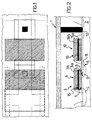
- an EEPROM cell of the FLOTOX type with two levels of polysilicon which cell is integrated in a conductive substrate 2 of the P type.
- the memory cell 1 comprises a floating gate MOS transistor 3 and an associated selection transistor 10 for selecting a cell to be programmed from a group of cells in a memory matrix.
- the floating gate transistor 3 has a source region 4 and a drain region 5.
- a gate region 6 projects from the substrate 2.
- the gate region 6 is isolated from the surface of the substrate 2 by a layer 7 of gate oxide which has a thinner portion referred to as the tunnel oxide 8.
- the gate region 6 comprises conventionally a floating gate region 6a formed from a first layer 13 of polysilicon, and a control gate region 6b formed from a second polysilicon layer 14.
- An intermediate dielectric layer 15 provides insulation between the two gate regions 6a, 6b.
- the drain region 5 is formed, for example, by an implant of the N type.
- the drain region 5 is formed using an LDD implanting technique.
- the drain region 5 is formed, for example, by an N-type implant in the substrate 2. Formed at this drain region 5 is a more heavily doped region 9 of the N+ type which extends to beneath the tunnel region 8.
- the source region 4 of the cell 1 is formed by implanting the substrate 2 with dopant of the N+ type.
- the source region 4 is formed concurrently with the process step for forming the heavily doped regions 9.
- the selection transistor 10 has a source region 11 which is coincident with the drain region 5 of the floating gate transistor 3, and has a drain region 12 formed in the substrate 2.
- the drain region 12 is formed, for example, by an N-type implant.
- the drain region 12 is formed using an LDD implanting technique.
- the gate region 16 includes conventionally two overlapping polysilicon regions 16a, 16b formed in the first and second layers 13, 14 of polysilicon, respectively, with the interposition of the intermediate dielectric layer 15; the two regions 16a, 16b are then short-circuited outside the cell.
- the method of this invention for forming said cell 1, is formed by carrying out a first selective implantation of the N+ type to form a source region 4 of the floating gate MOS transistor 3 and a heavily doped region 9 of the N+ type.
- a first oxide layer 7 of a first thickness, for forming the gate oxides of the cell 1, and a second oxide layer 8 of a second thickness smaller than that of the first layer 7, for forming the tunnel oxide of the cell 1 ( Figure 4), are then formed selectively.
- a self-aligned etching step is then carried out by a conventional photolithographic process wherein a photolithographic mask 17 is used to define the gates 6 and 16.
- a second implantation, of the N type, is effected to form the drain region of the floating gate transistor 3 and of the selection transistor 10.
- Spacers 18, and the drain contacts of the selection transistor 10 are then formed conventionally.
- FIG. 11 A second embodiment of the cell according to the invention is shown in Figures 11 and 12.
- the memory cell 1a comprises a floating gate MOS transistor 20 and an associated selection transistor 21.
- the floating gate transistor 20 has a source region 22, a drain region 23, and a gate region 24 including a floating gate region 24a and a control gate region 24b.
- the gate region 24a formed from a first polysilicon layer, is isolated from the surface of the substrate 2 by a layer 25 of gate oxide which has a thinner portion referred to as the tunnel oxide 26.
- the control gate region 24b formed from a second polysilicon layer, is coupled capacitively to the floating gate region 24a through an intermediate dielectric layer.
- the selection transistor 21 includes a drain region 28 and a gate region 27.
- the source region 23 of the selection transistor 21 is in common with the drain region of the floating gate transistor 20.
- This region 23 extends from the substrate 2 portion underlying the tunnel oxide 26 to the substrate 2 portion underlying the gate region 27 of the transistor 21.
- the region 23 is formed by an implant of the N+ type. In particular, the region is formed during the same process step as is devoted to forming the source region 22 of the floating gate transistor 20.
- the drain region 28 of the selection transistor 21 is formed by the same N+ implant as the source region 22.
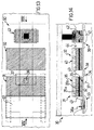
- Figures 13, 14 show a third embodiment of the inventive cell.
- a memory cell 30 comprises conventionally a floating gate transistor 31, and an associated selection transistor 32.
- the floating gate transistor 31 has source 33 and drain 34 regions, and a gate region 35 which comprises a floating gate region 25a and a control gate region 35b.
- the gate region 35a is formed from a first polysilicon layer, and is isolated from the substrate 2 by an oxide layer 36' which has a thinner portion or tunnel region 36.
- the control gate region 35b is formed from a second polysilicon layer and coupled capacitively to the floating gate region 35a through an intermediate dielectric layer.
- the gate region 35 comprises a silicide layer 38a.
- the drain region 34 is formed by an implant of the N- type in the substrate 2. Formed at this drain region 34 is a heavily doped region 37 of the N+ type which extends to beneath the tunnel region 36.
- the source region 33 of the cell 31 is formed by an N+ dopant implant in the substrate 2, on a portion whereof a silicide layer 38a is formed.
- the source region 33 and region 37 are formed by the same implanting step.
- the selection transistor 32 has a source region 38 of the N- type which is coincident with the drain region 34 of the floating gate transistor 31, a drain region 39 formed in the P-type substrate 2, and a gate region 40.
- the gate region 40 includes a silicide layer 38a.
- the region 39 also includes a contact region 41, formed by implantation of an N+ dopant.
- a contact head 42 is placed on this contact region.
- This head 42 includes a first portion formed from a first polysilicon layer and isolated from the region 41 by an oxide layer, and a second portion formed from a second polysilicon layer which is in direct contact with the region 41. Said first portion encircles said second portion. An oxide layer 42 may be provided between the first and second portions. The second portion is overlaid by a silicide layer 38a.
- Screening elements 43, 44 of a dielectric material are formed between the gate regions 35 and 40, and between the gate region 40 and the contact head 42.
- a spacer 45 also made of a dielectric material, is formed on the side of the gate region 35 facing toward the source region 33.
- This embodiment of the inventive memory cell is specially advantageous where the EEPROM cell fabrication process provides for the formation of silicide layers.
- this region and the gate regions of the cell can be silicidised without incurring a short circuit of the silicide layer provided on the source region to the substrate, as may instead occur where the source region is obtained by an LDD or N-type implantation according to the state of the art, and this without additional fabrication process steps.
Landscapes
- Non-Volatile Memory (AREA)
- Semiconductor Memories (AREA)
Priority Applications (4)
| Application Number | Priority Date | Filing Date | Title |
|---|---|---|---|
| DE69836423T DE69836423D1 (de) | 1998-06-30 | 1998-06-30 | Verfahren zur Herstellung einer EEPROM-Speicherzelle |
| EP98830390A EP0969507B1 (de) | 1998-06-30 | 1998-06-30 | Verfahren zur Herstellung einer EEPROM-Speicherzelle |
| US09/343,120 US6207990B1 (en) | 1998-06-30 | 1999-06-29 | Eeprom memory cell and corresponding manufacturing method |
| US09/760,069 US6548355B2 (en) | 1998-06-30 | 2001-01-11 | EEPROM memory cell and corresponding manufacturing method |
Applications Claiming Priority (1)
| Application Number | Priority Date | Filing Date | Title |
|---|---|---|---|
| EP98830390A EP0969507B1 (de) | 1998-06-30 | 1998-06-30 | Verfahren zur Herstellung einer EEPROM-Speicherzelle |
Publications (2)
| Publication Number | Publication Date |
|---|---|
| EP0969507A1 true EP0969507A1 (de) | 2000-01-05 |
| EP0969507B1 EP0969507B1 (de) | 2006-11-15 |
Family
ID=8236698
Family Applications (1)
| Application Number | Title | Priority Date | Filing Date |
|---|---|---|---|
| EP98830390A Expired - Lifetime EP0969507B1 (de) | 1998-06-30 | 1998-06-30 | Verfahren zur Herstellung einer EEPROM-Speicherzelle |
Country Status (3)
| Country | Link |
|---|---|
| US (2) | US6207990B1 (de) |
| EP (1) | EP0969507B1 (de) |
| DE (1) | DE69836423D1 (de) |
Cited By (1)
| Publication number | Priority date | Publication date | Assignee | Title |
|---|---|---|---|---|
| FR2834583A1 (fr) * | 2002-01-04 | 2003-07-11 | Samsung Electronics Co Ltd | Dispositif de memoire non volatile et procede de fabrication |
Families Citing this family (9)
| Publication number | Priority date | Publication date | Assignee | Title |
|---|---|---|---|---|
| US6812521B1 (en) * | 1999-11-16 | 2004-11-02 | Advanced Micro Devices, Inc. | Method and apparatus for improved performance of flash memory cell devices |
| JPWO2003028112A1 (ja) * | 2001-09-20 | 2005-01-13 | 株式会社ルネサステクノロジ | 半導体集積回路装置及びその製造方法 |
| JP2004014978A (ja) * | 2002-06-11 | 2004-01-15 | Renesas Technology Corp | 不揮発性半導体記憶装置 |
| US7585731B2 (en) * | 2004-02-20 | 2009-09-08 | Renesas Technology Corp. | Semiconductor integrated circuit device and its manufacturing method |
| TWI257169B (en) * | 2005-04-19 | 2006-06-21 | Powerchip Semiconductor Corp | Programmable and erasable digital switch device and manufacturing method and operating method thereof |
| US7382658B2 (en) * | 2006-01-26 | 2008-06-03 | Mosys, Inc. | Non-volatile memory embedded in a conventional logic process and methods for operating same |
| US20070170489A1 (en) * | 2006-01-26 | 2007-07-26 | Fang Gang-Feng | Method to increase charge retention of non-volatile memory manufactured in a single-gate logic process |
| CN102623455A (zh) * | 2011-01-27 | 2012-08-01 | 北京兆易创新科技有限公司 | 一种非易失性存储单元及其制造方法 |
| KR101334844B1 (ko) * | 2011-12-29 | 2013-12-05 | 주식회사 동부하이텍 | 싱글 폴리형 이이피롬과 그 제조 방법 |
Citations (6)
| Publication number | Priority date | Publication date | Assignee | Title |
|---|---|---|---|---|
| US4814854A (en) * | 1985-05-01 | 1989-03-21 | Texas Instruments Incorporated | Integrated circuit device and process with tin-gate transistor |
| JPH021176A (ja) * | 1988-03-18 | 1990-01-05 | Toshiba Corp | 不揮発性半導体記憶装置およびその製造方法 |
| EP0366423A2 (de) * | 1988-10-25 | 1990-05-02 | Matsushita Electronics Corporation | Verfahren zur Herstellung einer nicht-flüchtigen Speicheranordnung |
| US5326999A (en) * | 1991-11-19 | 1994-07-05 | Samsung Electronics, Co., Ltd. | Non-volatile semiconductor memory device and manufacturing method thereof |
| EP0655785A2 (de) * | 1993-11-30 | 1995-05-31 | Kabushiki Kaisha Toshiba | Nichtflüchtige Halbleiterspeicheranordnung und Verfahren zur Herstellung |
| EP0752721A2 (de) * | 1995-06-29 | 1997-01-08 | SHARP Corporation | Nichtflüchtiger Halbleiterspeicher und Verfahren zur Steuerung und Verfahren zu seiner Herstellung |
Family Cites Families (24)
| Publication number | Priority date | Publication date | Assignee | Title |
|---|---|---|---|---|
| US4701776A (en) * | 1983-08-29 | 1987-10-20 | Seeq Technology, Inc. | MOS floating gate memory cell and process for fabricating same |
| US4833096A (en) * | 1988-01-19 | 1989-05-23 | Atmel Corporation | EEPROM fabrication process |
| US4851361A (en) * | 1988-02-04 | 1989-07-25 | Atmel Corporation | Fabrication process for EEPROMS with high voltage transistors |
| US5017979A (en) * | 1989-04-28 | 1991-05-21 | Nippondenso Co., Ltd. | EEPROM semiconductor memory device |
| JPH0567791A (ja) | 1991-06-20 | 1993-03-19 | Mitsubishi Electric Corp | 電気的に書込および消去可能な半導体記憶装置およびその製造方法 |
| JPH05121756A (ja) | 1991-10-24 | 1993-05-18 | Mitsubishi Electric Corp | 半導体装置及びその製造方法 |
| JP2951082B2 (ja) | 1991-10-24 | 1999-09-20 | 株式会社東芝 | 半導体記憶装置およびその製造方法 |
| JPH05129614A (ja) | 1991-10-30 | 1993-05-25 | Mitsubishi Electric Corp | 電気的に書込および消去可能な半導体記憶装置の製造方法 |
| JPH05129620A (ja) * | 1991-11-08 | 1993-05-25 | Fujitsu Ltd | Eeprom装置の製造方法及びeeprom装置 |
| US5471422A (en) * | 1994-04-11 | 1995-11-28 | Motorola, Inc. | EEPROM cell with isolation transistor and methods for making and operating the same |
| US5440158A (en) * | 1994-07-05 | 1995-08-08 | Taiwan Semiconductor Manufacturing Company Ltd. | Electrically programmable memory device with improved dual floating gates |
| US5550072A (en) * | 1994-08-30 | 1996-08-27 | National Semiconductor Corporation | Method of fabrication of integrated circuit chip containing EEPROM and capacitor |
| US5619052A (en) * | 1994-09-29 | 1997-04-08 | Macronix International Co., Ltd. | Interpoly dielectric structure in EEPROM device |
| US5512503A (en) * | 1994-11-23 | 1996-04-30 | United Microelectronics Corporation | Method of manufacture of a split gate flash EEPROM memory cell |
| JPH08293564A (ja) * | 1995-04-20 | 1996-11-05 | Matsushita Electron Corp | 半導体記憶装置およびその製造方法 |
| JPH08330454A (ja) * | 1995-06-02 | 1996-12-13 | Sony Corp | 浮遊ゲート型不揮発性半導体記憶装置 |
| US5606521A (en) * | 1995-06-28 | 1997-02-25 | Philips Electronics North America Corp. | Electrically erasable and programmable read only memory with non-uniform dielectric thickness |
| JPH09106700A (ja) * | 1995-10-13 | 1997-04-22 | Sony Corp | 不揮発性メモリの検査方法 |
| US5998826A (en) * | 1996-09-05 | 1999-12-07 | Macronix International Co., Ltd. | Triple well floating gate memory and operating method with isolated channel program, preprogram and erase processes |
| JP2877103B2 (ja) * | 1996-10-21 | 1999-03-31 | 日本電気株式会社 | 不揮発性半導体記憶装置およびその製造方法 |
| KR100221619B1 (ko) * | 1996-12-28 | 1999-09-15 | 구본준 | 플래쉬 메모리 셀의 제조방법 |
| US5936274A (en) * | 1997-07-08 | 1999-08-10 | Micron Technology, Inc. | High density flash memory |
| TW359886B (en) * | 1997-09-02 | 1999-06-01 | United Microelectronics Corp | Electrostatic discharge protection device and production process therefor |
| US5918124A (en) * | 1997-10-06 | 1999-06-29 | Vanguard International Semiconductor Corporation | Fabrication process for a novel multi-storage EEPROM cell |
-
1998
- 1998-06-30 EP EP98830390A patent/EP0969507B1/de not_active Expired - Lifetime
- 1998-06-30 DE DE69836423T patent/DE69836423D1/de not_active Expired - Lifetime
-
1999
- 1999-06-29 US US09/343,120 patent/US6207990B1/en not_active Expired - Lifetime
-
2001
- 2001-01-11 US US09/760,069 patent/US6548355B2/en not_active Expired - Lifetime
Patent Citations (6)
| Publication number | Priority date | Publication date | Assignee | Title |
|---|---|---|---|---|
| US4814854A (en) * | 1985-05-01 | 1989-03-21 | Texas Instruments Incorporated | Integrated circuit device and process with tin-gate transistor |
| JPH021176A (ja) * | 1988-03-18 | 1990-01-05 | Toshiba Corp | 不揮発性半導体記憶装置およびその製造方法 |
| EP0366423A2 (de) * | 1988-10-25 | 1990-05-02 | Matsushita Electronics Corporation | Verfahren zur Herstellung einer nicht-flüchtigen Speicheranordnung |
| US5326999A (en) * | 1991-11-19 | 1994-07-05 | Samsung Electronics, Co., Ltd. | Non-volatile semiconductor memory device and manufacturing method thereof |
| EP0655785A2 (de) * | 1993-11-30 | 1995-05-31 | Kabushiki Kaisha Toshiba | Nichtflüchtige Halbleiterspeicheranordnung und Verfahren zur Herstellung |
| EP0752721A2 (de) * | 1995-06-29 | 1997-01-08 | SHARP Corporation | Nichtflüchtiger Halbleiterspeicher und Verfahren zur Steuerung und Verfahren zu seiner Herstellung |
Non-Patent Citations (1)
| Title |
|---|
| PATENT ABSTRACTS OF JAPAN vol. 014, no. 133 (E - 0902) 13 March 1990 (1990-03-13) * |
Cited By (1)
| Publication number | Priority date | Publication date | Assignee | Title |
|---|---|---|---|---|
| FR2834583A1 (fr) * | 2002-01-04 | 2003-07-11 | Samsung Electronics Co Ltd | Dispositif de memoire non volatile et procede de fabrication |
Also Published As
| Publication number | Publication date |
|---|---|
| US20010001294A1 (en) | 2001-05-17 |
| EP0969507B1 (de) | 2006-11-15 |
| DE69836423D1 (de) | 2006-12-28 |
| US6207990B1 (en) | 2001-03-27 |
| US6548355B2 (en) | 2003-04-15 |
Similar Documents
| Publication | Publication Date | Title |
|---|---|---|
| US6482698B2 (en) | Method of manufacturing an electrically programmable, non-volatile memory and high-performance logic circuitry in the same semiconductor chip | |
| US4451904A (en) | Semiconductor memory device | |
| US6534355B2 (en) | Method of manufacturing a flash memory having a select transistor | |
| US6159795A (en) | Low voltage junction and high voltage junction optimization for flash memory | |
| US6207991B1 (en) | Integrated non-volatile and CMOS memories having substantially the same thickness gates and methods of forming the same | |
| EP0969507B1 (de) | Verfahren zur Herstellung einer EEPROM-Speicherzelle | |
| US6124157A (en) | Integrated non-volatile and random access memory and method of forming the same | |
| EP0986100B1 (de) | Elektronisches Bauteil mit EEPROM-Speicherzellen, Hochspannungstransistoren und Niederspannungstransistoren mit Silizidanschlüssen, sowie Herstellungsverfahren desselben | |
| US20020053710A1 (en) | Semiconductor device having a high breakdown voltage | |
| US6268633B1 (en) | Electronic structure comprising high and low voltage transistors, and a corresponding fabrication method | |
| US6008093A (en) | Method of making a mask ROM | |
| JPH07202044A (ja) | 半導体装置の製造方法 | |
| US6344386B1 (en) | Method for fabricating semiconductor device including memory cell region and CMOS logic region | |
| US6127224A (en) | Process for forming a non-volatile memory cell with silicided contacts | |
| US6558997B2 (en) | Method for fabricating the control and floating gate electrodes without having their upper surface silicided | |
| EP0902466B1 (de) | Herstellungsverfahren eines nativen MOS-P-Kanal-Transistors mit Verfahren für nichtflüchtige Speicher | |
| EP0714133B1 (de) | Integrierte EEPROM-Schaltung mit reduziertem Substrat-Effekt und Zwei-Wannen-Herstellungsverfahren hiervon | |
| EP0204498A2 (de) | EEPROM-Zelle und Verfahren zur HerstellUng | |
| EP0892430B1 (de) | Herstellungsverfahren für einen integrierten Schaltkreis mit einer Speicherzellenmatrix | |
| US6278163B1 (en) | HV transistor structure and corresponding manufacturing method | |
| US6933199B1 (en) | Method for integrating non-volatile memory with high-voltage and low-voltage logic in a salicide process | |
| US20040217411A1 (en) | Non-volatile semiconductor memory device and manufacturing method therefor | |
| EP0962982A1 (de) | Schaltungsstruktur für Byte-Löschbare EEPROMs | |
| EP0930655A1 (de) | Festwertspeicherzelle und deren Herstellungsverfahren | |
| EP0987763A1 (de) | Transistor mit angeschlossener Diode und Herstellungsverfahren dazu |
Legal Events
| Date | Code | Title | Description |
|---|---|---|---|
| PUAI | Public reference made under article 153(3) epc to a published international application that has entered the european phase |
Free format text: ORIGINAL CODE: 0009012 |
|
| AK | Designated contracting states |
Kind code of ref document: A1 Designated state(s): DE FR GB IT |
|
| AX | Request for extension of the european patent |
Free format text: AL;LT;LV;MK;RO;SI |
|
| 17P | Request for examination filed |
Effective date: 20000313 |
|
| AKX | Designation fees paid |
Free format text: DE FR GB IT |
|
| 17Q | First examination report despatched |
Effective date: 20031217 |
|
| RTI1 | Title (correction) |
Free format text: EEPROM MEMORY CELL MANUFACTURING METHOD |
|
| GRAP | Despatch of communication of intention to grant a patent |
Free format text: ORIGINAL CODE: EPIDOSNIGR1 |
|
| GRAS | Grant fee paid |
Free format text: ORIGINAL CODE: EPIDOSNIGR3 |
|
| GRAA | (expected) grant |
Free format text: ORIGINAL CODE: 0009210 |
|
| AK | Designated contracting states |
Kind code of ref document: B1 Designated state(s): DE FR GB IT |
|
| REG | Reference to a national code |
Ref country code: GB Ref legal event code: FG4D |
|
| REF | Corresponds to: |
Ref document number: 69836423 Country of ref document: DE Date of ref document: 20061228 Kind code of ref document: P |
|
| PG25 | Lapsed in a contracting state [announced via postgrant information from national office to epo] |
Ref country code: DE Free format text: LAPSE BECAUSE OF FAILURE TO SUBMIT A TRANSLATION OF THE DESCRIPTION OR TO PAY THE FEE WITHIN THE PRESCRIBED TIME-LIMIT Effective date: 20070216 |
|
| ET | Fr: translation filed | ||
| PLBE | No opposition filed within time limit |
Free format text: ORIGINAL CODE: 0009261 |
|
| STAA | Information on the status of an ep patent application or granted ep patent |
Free format text: STATUS: NO OPPOSITION FILED WITHIN TIME LIMIT |
|
| 26N | No opposition filed |
Effective date: 20070817 |
|
| PGFP | Annual fee paid to national office [announced via postgrant information from national office to epo] |
Ref country code: GB Payment date: 20070530 Year of fee payment: 10 |
|
| PGFP | Annual fee paid to national office [announced via postgrant information from national office to epo] |
Ref country code: IT Payment date: 20070607 Year of fee payment: 10 |
|
| PGFP | Annual fee paid to national office [announced via postgrant information from national office to epo] |
Ref country code: FR Payment date: 20070627 Year of fee payment: 10 |
|
| GBPC | Gb: european patent ceased through non-payment of renewal fee |
Effective date: 20080630 |
|
| REG | Reference to a national code |
Ref country code: FR Ref legal event code: ST Effective date: 20090228 |
|
| PG25 | Lapsed in a contracting state [announced via postgrant information from national office to epo] |
Ref country code: GB Free format text: LAPSE BECAUSE OF NON-PAYMENT OF DUE FEES Effective date: 20080630 |
|
| PG25 | Lapsed in a contracting state [announced via postgrant information from national office to epo] |
Ref country code: IT Free format text: LAPSE BECAUSE OF NON-PAYMENT OF DUE FEES Effective date: 20080630 Ref country code: FR Free format text: LAPSE BECAUSE OF NON-PAYMENT OF DUE FEES Effective date: 20080630 |