EP0971416A1 - Speicheranordnung und verfahren zu deren herstellung, und integrierte schaltung und verfahren zur herstellung einer halbleiteranordnung - Google Patents
Speicheranordnung und verfahren zu deren herstellung, und integrierte schaltung und verfahren zur herstellung einer halbleiteranordnung Download PDFInfo
- Publication number
- EP0971416A1 EP0971416A1 EP99901180A EP99901180A EP0971416A1 EP 0971416 A1 EP0971416 A1 EP 0971416A1 EP 99901180 A EP99901180 A EP 99901180A EP 99901180 A EP99901180 A EP 99901180A EP 0971416 A1 EP0971416 A1 EP 0971416A1
- Authority
- EP
- European Patent Office
- Prior art keywords
- region
- insulating film
- forming
- memory device
- conduction
- Prior art date
- Legal status (The legal status is an assumption and is not a legal conclusion. Google has not performed a legal analysis and makes no representation as to the accuracy of the status listed.)
- Withdrawn
Links
Images









Classifications
-
- H—ELECTRICITY
- H10—SEMICONDUCTOR DEVICES; ELECTRIC SOLID-STATE DEVICES NOT OTHERWISE PROVIDED FOR
- H10B—ELECTRONIC MEMORY DEVICES
- H10B69/00—Erasable-and-programmable ROM [EPROM] devices not provided for in groups H10B41/00 - H10B63/00, e.g. ultraviolet erasable-and-programmable ROM [UVEPROM] devices
-
- B—PERFORMING OPERATIONS; TRANSPORTING
- B82—NANOTECHNOLOGY
- B82Y—SPECIFIC USES OR APPLICATIONS OF NANOSTRUCTURES; MEASUREMENT OR ANALYSIS OF NANOSTRUCTURES; MANUFACTURE OR TREATMENT OF NANOSTRUCTURES
- B82Y10/00—Nanotechnology for information processing, storage or transmission, e.g. quantum computing or single electron logic
-
- H—ELECTRICITY
- H10—SEMICONDUCTOR DEVICES; ELECTRIC SOLID-STATE DEVICES NOT OTHERWISE PROVIDED FOR
- H10D—INORGANIC ELECTRIC SEMICONDUCTOR DEVICES
- H10D30/00—Field-effect transistors [FET]
- H10D30/60—Insulated-gate field-effect transistors [IGFET]
- H10D30/68—Floating-gate IGFETs
- H10D30/681—Floating-gate IGFETs having only two programming levels
- H10D30/683—Floating-gate IGFETs having only two programming levels programmed by tunnelling of carriers, e.g. Fowler-Nordheim tunnelling
-
- H—ELECTRICITY
- H10—SEMICONDUCTOR DEVICES; ELECTRIC SOLID-STATE DEVICES NOT OTHERWISE PROVIDED FOR
- H10D—INORGANIC ELECTRIC SEMICONDUCTOR DEVICES
- H10D30/00—Field-effect transistors [FET]
- H10D30/60—Insulated-gate field-effect transistors [IGFET]
- H10D30/69—IGFETs having charge trapping gate insulators, e.g. MNOS transistors
-
- H—ELECTRICITY
- H10—SEMICONDUCTOR DEVICES; ELECTRIC SOLID-STATE DEVICES NOT OTHERWISE PROVIDED FOR
- H10D—INORGANIC ELECTRIC SEMICONDUCTOR DEVICES
- H10D64/00—Electrodes of devices having potential barriers
- H10D64/01—Manufacture or treatment
- H10D64/031—Manufacture or treatment of data-storage electrodes
- H10D64/035—Manufacture or treatment of data-storage electrodes comprising conductor-insulator-conductor-insulator-semiconductor structures
-
- H—ELECTRICITY
- H10—SEMICONDUCTOR DEVICES; ELECTRIC SOLID-STATE DEVICES NOT OTHERWISE PROVIDED FOR
- H10D—INORGANIC ELECTRIC SEMICONDUCTOR DEVICES
- H10D84/00—Integrated devices formed in or on semiconductor substrates that comprise only semiconducting layers, e.g. on Si wafers or on GaAs-on-Si wafers
- H10D84/01—Manufacture or treatment
- H10D84/02—Manufacture or treatment characterised by using material-based technologies
- H10D84/03—Manufacture or treatment characterised by using material-based technologies using Group IV technology, e.g. silicon technology or silicon-carbide [SiC] technology
- H10D84/038—Manufacture or treatment characterised by using material-based technologies using Group IV technology, e.g. silicon technology or silicon-carbide [SiC] technology using silicon technology, e.g. SiGe
-
- H—ELECTRICITY
- H10—SEMICONDUCTOR DEVICES; ELECTRIC SOLID-STATE DEVICES NOT OTHERWISE PROVIDED FOR
- H10D—INORGANIC ELECTRIC SEMICONDUCTOR DEVICES
- H10D86/00—Integrated devices formed in or on insulating or conducting substrates, e.g. formed in silicon-on-insulator [SOI] substrates or on stainless steel or glass substrates
- H10D86/01—Manufacture or treatment
-
- H—ELECTRICITY
- H10—SEMICONDUCTOR DEVICES; ELECTRIC SOLID-STATE DEVICES NOT OTHERWISE PROVIDED FOR
- H10D—INORGANIC ELECTRIC SEMICONDUCTOR DEVICES
- H10D86/00—Integrated devices formed in or on insulating or conducting substrates, e.g. formed in silicon-on-insulator [SOI] substrates or on stainless steel or glass substrates
- H10D86/201—Integrated devices formed in or on insulating or conducting substrates, e.g. formed in silicon-on-insulator [SOI] substrates or on stainless steel or glass substrates the substrates comprising an insulating layer on a semiconductor body, e.g. SOI
-
- H—ELECTRICITY
- H10—SEMICONDUCTOR DEVICES; ELECTRIC SOLID-STATE DEVICES NOT OTHERWISE PROVIDED FOR
- H10D—INORGANIC ELECTRIC SEMICONDUCTOR DEVICES
- H10D88/00—Three-dimensional [3D] integrated devices
- H10D88/01—Manufacture or treatment
Definitions
- the present invention relates to a memory device for holding information by storing charges moved from a conduction region into a storage region and a method of manufacturing the memory device, and a method of manufacturing an integrated circuit and a semiconductor device in which memory device are integrated. More particularly, the invention relates to a memory device in which a storage region comprises a plurality of particulates (quantum dots), a method of manufacturing the memory device, and a method of manufacturing an integrated circuit and a semiconductor device.
- a storage region is formed on a conduction region formed on the surface of a single crystal silicon substrate with an insulating film in between. Charges moved from the conduction region by tunneling the insulating film are stored into the storage region, thereby information is held in a non-volatile memory. Hitherto, the storage region is formed by using a two-dimensionally spread continuous semiconductor film.
- a thermal oxide film made of silicon having excellent insulating properties is used as an insulating film between the conduction region and the storage region.
- the thermal oxide film is prepared by heating a single crystal silicon substrate to 800 to 1000 °C in an oxygen atmosphere.
- the silicon substrate is not deformed nor melt around this temperature. Since the thermal oxide film formed on the single crystal silicon substrate has excellent insulating properties, charges are not leaked from the two-dimensionally continued storage region and are stably held.
- the substrate in case of using the thermal oxide film as an insulating film between the conduction region and the storage region, the substrate has to be heated to a high temperature of 800 to 1000 °C.
- the substrate is made of glass or plastic material instead of single crystal silicon, however, such high-temperature heat treatment cannot be performed.
- the temperature at which a glass substrate is deformed is 500 °C.
- the temperature at which a plastic substrate is deformed is at most 200 °C even when the substrate is made of a heat resistant material.
- the insulating film between the conduction region and the storage region has to be prepared in low-temperature conditions of 500 °C or lower.
- an oxide film such as a silicon oxide film (SiO 2 ) on the silicon substrate is resistant to heat of high temperature
- the conduction region on the oxide film is made of polysilicon and the surface of polysilicon is rough. Due to the roughness of the polysilicon, concentration of an electric field occurs in the insulating film provided on the polysilicon, which causes a problem that the charges in the two-dimensionally continued storage region are also leaked from the position where concentration of an electric field occurs.
- the invention has been achieved in view of the above problems and its object is to provide a memory device which can be fabricated at a low temperature on a substrate made of glass or plastic and can hold information for a long time and a method of manufacturing the memory device, and a method of manufacturing an integrated circuit and a semiconductor device.
- a memory device comprising: a conduction region made of a semiconductor; a first impurity region provided adjacent to the conduction region; a second impurity region provided apart from the first impurity region and adjacent to the conduction region; a storage region comprised of a plurality of dispersed particulates, for storing charges moved from the conduction region; a tunnel insulating film provided between the storage region and the conduction region, through which charges can pass; a control electrode for controlling each of a charge quantity of the storage region and conductivity of the conduction region; and a control insulating film provided between the control electrode and the storage region, wherein that of the particulates in the storage region is higher than that of structural holes (pin holes) produced in the tunnel insulating film.
- another memory device comprising: a conduction region made of a semiconductor; a first impurity region provided adjacent to the conduction region; a second impurity region provided apart from the first impurity region and adjacent to the conduction region; a storage region comprised of a plurality of dispersed particulates, for storing charges moved from the conduction region; a tunnel insulating film provided between the storage region and the conduction region, through which charges can pass; a control electrode for controlling each of a charge quantity of the storage region and conductivity of the conduction region; and a control insulating film provided between the control electrode and the storage region, wherein the number of the particulates in the storage region is five or more.
- further another memory device comprising: a conduction region made of a semiconductor; a first impurity region provided adjacent to the conduction region; a second impurity region provided apart from the first impurity region and adjacent to the conduction region; a storage region comprised of a plurality of dispersed particulates, for storing charges moved from the conduction region; a tunnel insulating film provided between the storage region and the conduction region, through which charges can pass; a control electrode for controlling each of a charge amount of the storage region and conductivity of the conduction region for memory; and a control insulating film provided between the control electrode and the storage region, wherein the conduction region is formed by a polysilicon film having a surface roughness of 0.1 nm to 100 nm and the number of particulates in the storage region is larger than that of crystal grains in the conduction region.
- an integrated circuit comprising a plurality of memory device, wherein each of the memory device comprises: a conduction region made of a semiconductor; a source region provided adjacent to the conduction region; a drain region provided apart from the source region and adjacent to the conduction region; a storage region comprised of a plurality of dispersed particulates, for storing charges moved from the conduction region; a tunnel insulating film which is provided between the storage region and the conduction region, through which charges can pass; a control electrode for controlling a charge quantity of the storage region and the conductivity of the conduction region; and a control insulating film provided between the control electrode and the storage region; and has the structure such that the surface density of the particulates in the storage region is higher than that of structural holes (pin holes) produced in the tunnel insulating film, the control electrode of each of the memory device is connected to a word line, and a source-drain path of each memory device is connected between a bit line and a source line.
- each of the memory device comprises: a conduction
- a method of manufacturing a memory device comprises: a step of forming a conduction region by a semiconductor film on a substrate made of an insulating material; a step of forming a tunnel insulating film on the conduction region; a step of forming a storage region comprised of a plurality of particulates dispersed on the tunnel insulating film, with the surface density of the particulates being higher than that of structural holes (pin holes) in the tunnel insulating film; a step of forming a control insulating film on the storage region; a step of forming a control electrode on the control insulating film; and a step of forming a first impurity region adjacent to the conduction region, and a second impurity region apart from the first impurity region and adjacent to the conduction region.
- Another method of manufacturing a memory device comprises: a step of forming a conduction region made by a semiconductor film on a substrate made of an insulating material; a step of forming a tunnel insulating film on the conduction region; a step of forming a storage region having five or more particulates dispersed on the tunnel insulating film; a step of forming a control insulating film on the storage region; a step of forming a control electrode on the control insulating film; and a step of forming a first impurity region adjacent to the conduction region and a second impurity region apart from the first impurity region and adjacent to the conduction region.
- Further another method of manufacturing a memory device comprises: a step of forming a conduction region, made by a polysilicon film whose surface roughness is 0.1 nm to 100 nm, on a substrate made of an insulating material; a step of forming a tunnel insulating film on the conduction region; a step of forming a storage region having dispersed particulates, the number of which is larger than the number of crystal grains in the conduction region, on the tunnel insulating film; a step of forming a control insulating film on the storage region; a step of forming a control electrode on the control insulating film; and a step of forming a first impurity region adjacent to the conduction region and a second impurity region apart from the first impurity region and adjacent to the conduction region.
- Further another method of manufacturing a memory device comprises: a step of forming a control electrode on a substrate made of an insulating material; a step of forming a control insulating film on the control electrode; a step of forming a storage region comprised of a plurality of dispersed particulates on the control insulating film, with the surface density of the particulates being higher than that of structural holes (pin holes) in the tunnel insulating film; a step of forming a tunnel insulating film on the storage region; a step of forming a conduction region made of a semiconductor on the tunnel insulating film; and a step of forming a first impurity region adjacent to the conduction region and a second impurity region apart from the first impurity region and adjacent to the conduction region.
- Further another method of manufacturing a memory device comprises: a step of forming a control electrode on a substrate made of an insulating material; a step of forming a control insulating film on the control electrode; a step of forming a storage region comprised of five or more dispersed particulates on the control insulating film; a step of forming a tunnel insulating film on the storage region; a step of forming a conduction region made of a semiconductor on the tunnel insulating film; and a step of forming a first impurity region adjacent to the conduction region and a second impurity region apart from the first impurity region and adjacent to the conduction region.
- Further another method of manufacturing a memory device comprises: a step of forming a control electrode on a substrate made of an insulating material; a step of forming a control insulating film on the control electrode; a step of forming a storage region comprised of a plurality of dispersed particulates on the control insulating film; a step of forming a tunnel insulating film on the storage region; a step of forming a conduction region made of a semiconductor on the tunnel insulating film; and a step of forming a first impurity region adjacent to the conduction region and a second impurity region apart from the first impurity region and adjacent to the conduction region, wherein the conduction region is formed by a polysilicon film having the surface roughness of 0.1 nm to 100 nm and the number of particulates in the storage region is set to be larger than the number of crystal grains in the conduction region.
- a method of manufacturing a semiconductor device comprises: a step of forming a semiconductor film on a substrate and, after that, forming a film for forming a storage region of a nonstoichiometric composition, excessively containing a semiconductor element, on the semiconductor film; and a step of forming a storage region by dispersing the particulates of a semiconductor in the film for forming a storage region by performing heat treatment.
- the "nonstoichiometric composition” denotes a composition having a ratio of components out of the stoichiometric composition. In the invention, it denotes a case where a ratio of components is out of the range of the stoichiometric composition so as to contain an excessive semiconductor.
- the size of each of the particulates constructing the storage region lies within the range from 1 nm to 10 nm. As an example, silicon (Si), germanium (Ge), and the like can be used.
- the semiconductor device by performing heat treatment such as irradiation of an energy beam to the film for forming a storage region of a nonstoichiometric composition containing a semiconductor excessively, the particulates in the semiconductor are dispersed in the film for forming a storage region, and a storage region is thus formed.
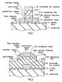
- Fig. 1 shows a basic structure of a memory device according to a first embodiment of the invention.
- a case where electrons are used as charges will be described as an example.
- holes are used as charges, the following description is the same as the case except that the sign of a potential is to be reversed.
- the memory device has a structure comprising a conduction region 13c and a first impurity region 13a and a second impurity region 13b adjacently formed on both sides of the conduction region 13c configured on a buffer layer 12 formed on a substrate 11 made of a non-silicon material such as quartz, glass, or plastic and so on.
- the buffer layer 12 is comprised of an insulating film made of SiO 2 or SiaN 4 , and so on.
- Each of the first impurity region 13a, the second impurity region 13b, and the conduction region 13c is comprised of, for example, a polysilicon layer 13 having a thickness of about tens of nm.
- Each of the first and second impurity regions 13a and 13b is formed by adding a Group V element such as phosphorus (P) as an n-type impurity, or a Group III element such as boron (B) as a p-type impurity to the polysilicon layer 13.
- P phosphorus
- B boron
- Each of the first impurity region 13a and the second impurity region 13b and the conduction region 13c can be made of any semiconductor (non-single crystal semiconductor) except single crystal semiconductor. It can be made of, for example, amorphous Si x Ge 1-x (0 ⁇ x ⁇ 1) or polycrystal Si x Ge 1-x (0 ⁇ x ⁇ 1).
- An insulating film 14 is provided in a corresponding position right on the conduction region 13c.
- the insulating film 14 consists of a tunnel insulating film 14a and a control insulating film 14b stacked on the tunnel insulating film 14a.
- Each of the tunnel insulating film 14a and the control insulating film 14b is made of SiO 2 , Si 3 N 4 , SiN k O 1 (k, 1 ⁇ 0), or the like.
- a storage region 15 is provided between the tunnel insulating film 14a and the control insulating film 14b to hold charges (electrons in this case).
- the thickness of the tunnel insulating film 14a is provided in a size (for example, less than 5 nm) that electrons can pass through the tunnel insulating film 14a into the storage region 15 by a quantum-mechanical tunnel effect.
- the storage region 15 is comprised of more than one particulates (quantum dots) 15a discretely disposed.
- the particulates 15a is formed of semiconductor particulates made of Si y Ge 1-y (0 ⁇ y ⁇ 1), SiFe 2 , Group II-VI compound, Group III-V compound, or the like, metal particulates made of Au, Sb, Sn, or the like, or insulator particulates made of SiN 2 (z ⁇ 0) or the like.
- the number of particulates 15a is larger than that (surface density) of structural holes (pin holes) opened in the tunnel insulating film 14a during the manufacturing process and is, specifically, five or more.
- the surface of the polysilicon layer 13 is rough. In the embodiment, it is preferable that the roughness is within the range from 0.1 nm to 100 nm and that the number of particulates 15a in the storage region 15 is larger than the number of crystal grains in the conduction region 13c.
- a control electrode 16 is formed on the insulating film 14, that is, in the position opposite to the conduction region 13c positioning the storage region 15 in the middle.
- the control electrode 16 is formed by a low-resistant polysilicon layer in which a metal such as aluminum (Al) or an impurity is doped.
- Al aluminum
- an electric field is applied between the conduction region 13c and the storage region 15, controlling the conductivity of the conduction region 13c and the number of electrons in the storage region 15.
- the thickness of the control insulating film 14b between the control electrode 16 and the storage region 15 is provided in a size (for example 50 nm or thicker) that the electrons cannot pass through the control insulating film 14b by the quantum-mechanical tunnel effect.
- the potential applied to the second impurity region 13b is set to the same (0V) as that applied to the first impurity region 13a or a potential (for example, 10V) higher than the potential applied to the first impurity region 13a is applied, and a potential (for example, 20V) higher than that applied to the first impurity region 13a is applied to the control electrode 16. Consequently, charges (electrons) in the conduction region 13c pass through the tunnel insulating film 14a, placed between the conduction region and the storage region, by the quantum-mechanical tunnel effect and are stored in more than one particulates 15a dispersed in the storage region 15. In such a manner, information is written.
- the potential to the second impurity region 13b is set to the same (0V) as that applied to the first impurity region 13a or a potential (for example, -10V) lower than that applied to the first impurity region 13a is applied, and a potential (for example, -20V) lower than that applied to the first impurity region 13a is applied to the control electrode 16. Consequently, charges (holes) in the conduction region 13c pass through the tunnel insulating film 14a, provided between the conduction region and the storage region, by the quantum-mechanical tunnel effect and are stored in more than one particulates 15a dispersed in the storage region 15. In such a manner, information is written. The information written as mentioned above is held by setting the potential to all of the electrodes to the same or keeping them in a floating state.
- the storage region 15 is comprised of the five or more dispersed particulates 15a in the memory device of the embodiment as described above, even when charges stored in some of the particulates 15a are leaked due to a structural defect occurring in the tunnel insulating film 14a, the charges stored in the particulates 15a formed in the region without any defect in the tunnel insulating film 14a are not leaked. In the embodiment, therefore, the information stored in the storage region 15 can be held for a long time. This is similarly applied to a case where the roughness of the surface of the polysilicon layer 13 is within the range from 0.1 nm to 100 nm and the number of particulates 15a in the storage region 15 is larger than that of crystal grains in the conduction region 13c.
- the tunnel insulating film can be formed by a low-temperature process, enabling the usage of an inexpensive material such as glass or plastic as the substrate.
- the written information is erased in such a manner that, when the first and second impurity regions 13a and 13b are of the n-type, while the potential applied to the second impurity region 13b is set to the same as that applied to the first impurity region 13a, a potential (for example, -20V) lower than that applied to the first impurity region 13a is applied to the control electrode 16, thereby making the charges (electrons) held in the storage region 15 move into the conduction region 13c passing through the tunnel insulating film 14a provided between the conduction region and the storage region.
- a potential for example, -20V
- the potential applied to the second impurity region 13b is set to the same as that applied to the first impurity region 13a and a potential (for example, 20V) higher than that applied to the first impurity region 13a is applied to the control electrode 16.
- a potential for example, 20V
- the written information is read out by measuring the conductivity of the conduction region 13c with respect to the potential of the control electrode 16 or the current value detecting a change in charge amount in the storage region 15.
- Fig. 2 shows the structure of a memory device according to a second embodiment of the invention.
- a control electrode 26 is provided on a substrate 21 made of, for example, quartz having a buffer layer 22 in between which is comprised of an insulating film made of SiO 2 , Si 3 N 4 , or the like.
- An insulating film 24 is formed on the buffer layer 22 and the control electrode 26.
- the insulating film 24 is comprised of an control insulating film 24b and a tunnel insulating film 24a stacked on the control insulating film 24b. Between the tunnel insulating film 24a and the control insulating film 24b, a storage region 25, comprised of more than one particulates 25a discretely disposed, is provided.
- a conduction region 23c is provided, with a first impurity region 23a and a second impurity region 23b. The first impurity region 23a and the second impurity region 23b are adjacent to the conduction region 23c.
- the first and second impurity regions 23a and 23b and the conduction region 23c are formed a polysilicon layer 23.
- the memory device of the embodiment is the bottom-gate type
- the memory device of the first embodiment is what is called the top-gate type
- other structures, actions (the methods of writing and erasing information, and methods of holding and reading information), and effects are substantially the same as those of the first embodiment. Their description is consequently omitted here.
- Figs. 3 and 4 are circuit construction diagrams for explaining the first method of integrating the memory device. According to the first method, while a gate electrode in each memory device is connected to a word line, a source-drain path is connected between a bit line and a source line, and a plurality of memory device are arranged in parallel.
- Fig. 5 shows a circuit construction when the memory device are integrated by the second method. According to the second method, while the gate electrode of each memory device is connected to a word line, the source-drain path is connected between a bit line and a source line, and a plurality of memory device are arranged in series. The operations of the memory units integrated by the methods will be described hereinafter.
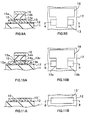
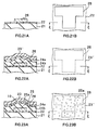
- each of the diagrams B is a plan view and each of the diagrams A is a cross section taken along the line ⁇ - ⁇ of the diagram B.
- the buffer layer 12 which is comprised of an Si 3 N 4 layer or an SiO 2 layer having a thickness of, for example, about 100 nm is formed by, for example, CVD (Chemical Vapor Deposition) or sputtering on an insulating substrate such as the substrate 11 made of quartz, glass, plastic, or the like.
- CVD Chemical Vapor Deposition
- the substrate temperature is set to 600 to 700 ° C and the polysilicon layer 13 having a thickness of about 10 nm is formed by, for example, CVD or sputtering.
- device isolation is performed by etching. At this time, defects of holes (pin holes) 10 occur in the polysilicon layer 13.
- a thermal oxidation or an oxidizing method of exposing the surface of the substrate to an oxygen ionized gas, generated by introducing oxygen into an alternating current electromagnetic field the surface of the polysilicon layer 13 (conduction region Ch1) is oxidized only by the thickness of about 10 nm, thereby making the tunnel insulating film 14a formed.
- a plurality of holes pin holes occur as mentioned above in the tunnel insulating film 14a due to the holes 10 in the polysilicon layer 13.
- Si x Ge 1-x (0 ⁇ x ⁇ 1) is deposited on the tunnel insulating film 14, thereby forming the storage region 15 comprised of more than one particulates 15a.
- the number of the particulates 15a at this time is set so that the coverage factor of the surface of the tunnel insulating film 14a is smaller than 1.
- the number of particulates is set to 5 or larger so that the surface density is higher than that of the defects occurred in the tunnel insulating film 14a.
- control insulating film 14b having a thickness of about 100 nm is formed.
- control electrode (gate electrode) 16 is formed by using polysilicon or a metal such as Al (aluminum), or Cu (copper), or W (tungsten) in a position opposite to the conduction region 13c (polysilicon layer 13) provided on the control insulating film 14b.
- the control electrode 16 is selectively etched until the surface of the conduction region (polysilicon layer 13) by RIE (Reactive Ion Etching) using a mixture gas of CF 4 (carbon tetrafluoride) and H 2 (hydrogen).
- ion implantation is performed by using the control electrode 16 as a mask, thereby forming the first impurity region 13a and the second impurity region 13b in the polysilicon layer 13.
- the ion implantation is carried out by ion implanting Group V atoms such as phosphorus (P) atoms when electrons are used as conduction charges ,or by ion implanting Group III atoms such as boron (B) atoms when holes are used as conduction charges.
- Group V atoms such as phosphorus (P) atoms when electrons are used as conduction charges
- Group III atoms such as boron (B) atoms when holes are used as conduction charges.
- the first impurity region 13a and the second impurity region 13b may also be formed by the polysilicon layer 13 being irradiated with an ionized gas containing the Group V atoms such as an ionized gas of PH 3 when electrons are used as conduction charges, or with an ionized gas containing the group III atoms such as an ionized gas of B 2 H 6 when holes are used as conduction charges, with the control electrode 16 being used as a mask. After that, the element is heated by using a furnace or an excimer laser, thereby activating the implanted impurities.
- an ionized gas containing the Group V atoms such as an ionized gas of PH 3 when electrons are used as conduction charges
- an ionized gas containing the group III atoms such as an ionized gas of B 2 H 6 when holes are used as conduction charges
- a protective film made of Si 3 N 4 or SiO 2 is formed by, for example, CVD or sputtering on the surface of the memory device formed as mentioned above.
- each diagram B is a plan view
- each diagram A is a cross section taken along the line ⁇ - ⁇ of diagram B.
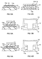
- the buffer layer 12 comprised of the Si 3 N 4 layer or the SiO 2 layer having a thickness of about 100 nm is formed made of quartz or the like by CVD or sputtering on the substrate 11. Subsequently, by plasma CVD (Plasma Enhanced Chemical Vapor Deposition; PECVD) or sputtering, an amorphous silicon layer 13' having a thickness of about tens of nm is formed at a temperature at which no deformation occurs in the substrate 11, and then device isolation is performed by etching.
- PECVD Plasma Enhanced Chemical Vapor Deposition
- the surface of the amorphous silicon layer 13' is oxidized by the plasma oxidizing method
- the tunnel insulating film 14a which is comprised of an SiO x layer (x ⁇ 2) having a thickness of tens of nm is formed on the surface of the amorphous silicon layer 13' by PECVD
- an XeCl excimer laser is irradiated by about 150 to 300 mJ/cm 2 to crystallize the amorphous silicon layer 13', thereby obtaining the polysilicon layer 13.
- excessive silicon in SiO x is deposited forming the storage region 15 comprised of many particulates 15a.
- the storage region 15 may be formed so that the coverage factor is smaller that 1 by CVD using, as materials, a gas containing silicon atoms such as silane or disilane and a gas containing germanium atoms such as germane or, by sputtering using silicon, or germanium, or a metal as a material.
- the control insulating film 14b having a thickness of about 100 nm is formed.
- the control electrode 16 is formed by using polysilicon or a metal such as Al, Cu, or W, in a position opposite to the conduction region 13c in the polysilicon layer 13, provided on the control insulating film 14b.
- the control insulating film 14b is selectively etched until the surface of the conduction region (polysilicon layer 13) by RIE using a mixture gas of CF 4 and H 2 .
- ion implantation is performed by using the control electrode 16 as a mask, thereby forming the first impurity region 13a and the second impurity region 13b in the polysilicon layer 13.
- the ion implantation is carried out by ion implanting Group V atoms such as phosphorus (P) atoms when electrons are used as conduction charges, or by Group III atoms such as boron (B) atoms when holes are used as conduction charges.
- Group V atoms such as phosphorus (P) atoms when electrons are used as conduction charges
- Group III atoms such as boron (B) atoms when holes are used as conduction charges.
- the polysilicon layer 13 is irradiated with an ionized gas containing the Group V atoms such as an ionized gas of PH 3 when electrons are used as conduction charges, or with an ionized gas containing the group III atoms such as an ionized gas of B 2 H 6 when holes are used as conduction charges by using the control electrode 16 as a mask, thereby enabling the first and second impurity regions 13a and 13b to be formed.
- the element is heated by using a furnace or an excimer laser, thereby activating the implanted impurities.
- a protective film made of Si 3 N 4 or SiO 2 is formed by, for example, CVD or sputtering on the surface of the memory device formed as described above.
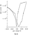
- Fig. 15 shows gate voltage - drain current characteristics (memory effects) of the memory device fabricated in the embodiment.
- the drain voltage is 5V.
- the memory device is obtained in such a manner that an SiO 0.5 layer is formed by PECVD and an XeCl excimer laser having the energy density of 260 mJ/cm 2 is irradiated, thereby forming the storage region consisting of Si dots in the SiO 0.5 layer.
- ion implantation of phosphorus (P) is carried out by PH 3 plasma irradiation, thereby forming the first and second impurity regions and, further, annealing by the XeCl excimer laser (210 mJ/cm 2 ) is performed to activate the implanted impurities.
- each diagram B is a plan view and each diagram A is a cross section taken along the line ⁇ - ⁇ of diagram B.
- the buffer layer 12 comprised of the Si 3 N 4 layer or SiO 2 layer having a thickness of about 100 nm is formed by CVD or sputtering on the substrate 11 made of quartz or the like. Subsequently, by PECVD or sputtering, an amorphous silicon layer, with which an n-type or p-type impurity is doped and which has a thickness of about tens of nm, is formed at a temperature at which no deformation occurs in the substrate 11. By etching, the amorphous silicon layer is selectively removed and the first impurity region 13a and the second impurity region 13b are formed.
- the amorphous silicon layer 13' which does not contain the impurity is formed on the surface of the substrate 11 by PECVD or sputtering and, after that, the region except for the conduction region 13c and the region corresponding to the first and second impurity regions 13a and 13b is selectively etched.
- the amorphous silicon layer 13' is irradiated with the XeCl excimer laser within the range of 150 to 300 mJ/cm 2 so as to be crystallized, thereby obtaining the polysilicon layer 13.
- the surface of the polysilicon layer 13 is oxidized by the plasma oxidizing method, and the tunnel insulating film 14a comprised of the SiO x layer (x ⁇ 2) having a thickness of tens of nm is formed by PECVD on the surface of the polysilicon layer 13 and, after that, an XeCl excimer laser is irradiated by about 150 to 300 mJ/cm 2 . Consequently, excessive silicon in SiO x is deposited forming the storage region 15 comprised of many particulates 15a.
- the storage region 15 having the coverage factor smaller than 1 may be formed by CVD using, as materials, a gas containing silicon atoms such as silane or disilane and a gas containing germanium atoms such as germane, or by sputtering using silicon, germanium, or a metal as a material as in the first method.
- the control insulating film 14b having a thickness of about 100 nm is formed.
- the control electrode 16 is formed by using polysilicon or a metal such as Al, Cu, or W in a position opposite to the conduction region 13c (polysilicon layer 13) provided on the control insulating film 14b.
- the control insulating film 14b is selectively etched until the surface of the conduction region (polysilicon layer 13) by RIE using a mixture gas of CF 4 and H 2 .
- the element is heated by using a furnace or an excimer laser, thereby activating the implanted impurities.
- a protective film made of Si 3 N 4 or SiO 2 is formed on the surface of the memory device formed as mentioned above by, for example, CVD or sputtering.
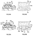
- Each of the diagrams B is a plan view and each of the diagrams A is a cross section taken along the line ⁇ - ⁇ of the diagram B.
- the buffer layer 22 comprised of an Si 3 N 4 layer, or an SiO 2 layer, or an SiN k O 1 layer (k, 1 ⁇ 0) having a thickness of, for example, about 100 nm is formed on the substrate 21 made of quartz, glass or plastic by, for example, CVD or sputtering.
- a metal film made of W (tungsten), Ta (tantalum), Mo (molybdenum), or the like is deposited by, for example, electron beam deposition and is patterned, thereby forming the control electrode 26.
- control insulating film 24b comprised of an SiO 2 layer having a thickness of about 100 nm, the tunnel insulating film 24a which is an SiO x (x ⁇ 2) layer having a thickness of about tens of nm, and an amorphous silicon layer 23' having a thickness of about tens of nm to which no impurity is added, are formed in accordance with this order.
- the amorphous silicon layer 23' is crystallized, thereby forming the polysilicon layer 23.
- excessive silicon in SiO x is deposited forming the storage region 25 comprised of many particulates 25a is formed in the tunnel insulating film 24a.
- device isolation is performed by selectively removing the polysilicon layer 23 and the tunnel insulating film 24a by, for example, RIE.
- a mask 27 made of photoresist or SiO 2 is formed on the polysilicon layer 23 in a region opposite to the control electrode 26.
- ion implantation is performed by using the mask 27, thereby forming the first impurity region 23a and the second impurity region 23b in the polysilicon layer 23.
- the ion implantation is carried out by ion implanting Group V atoms such as phosphorus (P) atoms, when electrons are used as conduction charges, or Group III atoms such as boron (B) atoms when holes are used as conduction charges.
- the first and second impurity regions 23a and 23b may be formed by the polysilicon layer 23 being irradiated with an ionized gas containing the Group V atoms such as an ionized gas of PH 3 when electrons are used as conduction charges, or with an ionized gas containing the group III atoms such as an ionized gas of B 2 H 6 when holes are used as conduction charges, using the mask 27.
- the element is heated by using a furnace or an excimer Laser to activate the implanted impurities.
- a protective film made of Si 3 N 4 or SiO 2 is formed by, for example, CVD or sputtering on the surface of the memory device formed as described above.
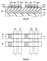
- FIG. 26 is a plan view of an actual device to which the invention of the circuit diagram shown in Fig. 3 is applied.
- Fig. 27 is a cross section taken along the line ⁇ - ⁇ of Fig. 26.
- each of source lines S 1 and S 2 , bit lines B 1 and B 2 , and word lines W 1 and W 2 is formed by a polysilicon layer to which metal such as Al or Cu or impurity is implanted.
- metal such as Al or Cu or impurity is implanted.
- the electrodes (G) for control of the memory device are connected to the word lines W1, W2, ... and a plurality of memory device each having a source-drain path connected between the bit line and the source line are arranged in parallel. It is sufficient to apply the potentials of the source line, bit line, and word line to the first impurity region, gate region, and the second impurity region as mentioned above, in order to write, erase, hold, and read out information with respect to each of the memory device.
- the control electrode of the memory device is connected to the word line and a plurality of memory device, in which the source-drain paths are connected between the bit line and the source line, are arranged in series. It is sufficient to apply the potentials of the source line, bit line, and word line to the first impurity region, gate region, and second impurity region of each memory device as mentioned above in order to write, erase, hold, and read out information with respect to each of the memory device.
- Fig. 28 shows an example of the structure of a memory unit obtained by integrating bottom-gate type memory device according to the fourth embodiment of the invention.
- the structure in plan view is similar to that in Fig. 26.
- Fig. 28 corresponds to the structure in cross section taken along the line ⁇ - ⁇ of Fig. 26.
- the method of manufacturing each element is as described above. When the elements are integrated as well, the integrated memory unit can be easily diverted. Consequently, its specific description is omitted here.
- Figs. 29 and 30 represent an example of the structure of a memory unit using top-gate type memory device according to a fifth embodiment of the invention.
- Fig. 29 is a plan view of an actual device to which the invention of the circuit diagram of Fig. 3 is applied.
- Fig. 30 is a cross section taken along the line ⁇ - ⁇ of Fig. 29.
- the source lines S 1 and S 2 , bit lines B 1 and B 2 , and word lines W 1 and W 2 are formed by a polysilicon layer to which a metal such as Al or Cu or impurity is implanted.
- Fig. 31 shows an example of integrating bottom-gate type memory device according to the second embodiment.
- V p for example, 10V
- V p for example, 5V
- a potential of only V p /2 should be applied to the source line S i and the bit line B i (i # m).
- OV is applied to the source line S m and the word lines except for the word line W n
- a potential of -V p (for example, -10V) is applied to the word line W n
- a potential -V d (for example, -5V) is applied to the bit line B m .
- a potential of only -V p /2 should be applied to the source line S m and the bit lines except for the bit line B m .
- the potential of all of electrodes is set to the same or in a floating state.
- 0V When reading the information from the memory device C nm , 0V is applied to all of the source lines and the bit lines except for the bit line B m , 0V is applied to the word lines except for the word line W n , a potential V r (for example, 5V) is applied to the word line W n , a potential V d (for example, 5V) is applied to the bit line B m , and a current passing the bit line B m is measured.
- V r for example, 5V
- V d for example, 5V
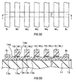
- Figs. 32 and 32 show an example of the structure of a memory unit using top-gate type memory device according to the sixth embodiment of the invention.
- Fig. 32 is a plan view of an actual device to which the invention of the circuit diagram shown in Fig. 5 is applied.
- Fig. 33 is a cross section taken along the line l-l of Fig. 32.
- the source line S 1 , bit line B 1 , and word lines W 1 , W 2 , W 3 , W 4 , ..., W n are formed by the polysilicon layer, to which a metal such as Al, Cu or impurity is implanted, as well.
- Fig. 34 shows an example in which bottom-gate type memory device according to the second embodiment are integrated. In a manner similar to Fig. 33, Fig. 34 corresponds to the cross section taken along the line l-l of Fig. 32.
- a memory device M nm (refer to Fig. 5) in the memory unit according to the embodiment will be described.
- the memory device has the n-type conductivity. Description of the case of a memory device having the p-type conductivity is omitted here.
- V p for example, 10V
- V p /2 for example, 5V
- V p /2 for example, 5V
- 0V When erasing the information written in the memory device M nm , 0V is applied to all of source lines, a potential -V p (for example, -10V) is applied to the word line W m , V p /2 (for example, 5V) is applied to word lines except for the word line W m , 0V is applied to the bit line B n , and -V p /2 (for example, -5V) is applied to bit lines in a memory device line including memory device whose gates are connected to the word line W m except for the bit line B n .
- V p /2 for example, 5V
- the potential to all of electrodes is set to the same or in a floating state.
- 0V is applied to all of the source lines and the bit lines except for the bit line B n
- 0V is applied to the word lines except for the word line W m
- 0V is applied to the word line W n
- a potential V d (for example, 5V) is applied to the bit line B m
- a current passing through the bit line B m is measured.
- a method of simultaneously fabricating memory device, according to the first embodiment (Fig. 1), and a peripheral circuit such as a control circuit on the same substrate will be described.
- an Si 3 N 4 and SiO 2 layers having a thickness of about 100 nm is formed as the buffer layer 12 by CVD or sputtering on the substrate 11 made of quartz, glass or plastic.
- the amorphous silicon layer 13' of tens of nm is formed by PECVD or sputtering on the surface of the buffer layer 12 at a temperature at which no deformation occurs in the substrate, and device isolation is performed by etching.
- an SiO x (x ⁇ 2) layer having a thickness of tens of nm is formed on the tunnel insulating film 14a by PECVD.
- irradiation of about 150 to 300 mJ/cm 2 is performed by the XeCl excimer laser. Consequently, as shown in Fig. 36, while the amorphous silicon layer 13' is crystallized and becomes the polysilicon layer 13, excessive silicon in SiO x is deposited forming the storage region 15 comprised of many particulates 15a.
- the memory device side (left half of the diagram) is covered with a photoresist film 17, and the storage region formed on the peripheral circuit side (right half of the diagram) is selectively removed by RIE using a mixture gas of SF 6 or CF 4 . and H 2 . After that, the photoresist film 17 is removed.
- the control insulating film 14b having a thickness of about 100 nm is formed.
- the control electrodes 16 (G m , G) are formed on the control insulating film 14b using a polysilicon layer or a metal such as Al, Cu, or W.
- etching is performed by RIE using a mixture gas of CF 4 and H 2 until the surface of the polysilicon layer 13 using the contorol electrodes 16 (G m , G) as masks.
- ion implantation is performed with the Group V atoms such as phosphorus when electrons are used as conduction charges, or with the Group III atoms such as boron when holes are used as conduction charges, thereby forming the first impurity regions 13a (S m , S) and the second impurity regions 13b (D m , D).
- the first impurity regions 13a (S m , S) and the second impurity regions 13b (D m , D) are formed.
- the elements are heated by using a furnace or an excimer laser to activate the implanted impurities.
- necessary wiring is carried out, and the surface of the substrate is covered with Si 3 N 4 or SiO 2 by CVD or by sputtering, thereby forming a protective film.
- a method of fabricating a peripheral circuit simultaneously with memory device according to the second embodiment (Fig. 2) on the same substrate will be described.
- the buffer layer 22 made of Si 3 N 4 or SiO 2 having a thickness of about 100 nm is formed on the substrate 21 made of quartz or the like by CVD or sputtering. After that, a film made of tungsten, tantalum, molybdenum, or the like is formed by electron beam deposition or sputtering and patterned, thereby forming the control electrodes 26 (G m , G).
- control insulating film 24b made of SiO 2 having a thickness of about 100 nm by using CVD or sputtering an SiO x (x ⁇ 2) layer 27 having a thickness of tens of nm is formed.
- the memory device side (left side in the diagram) is covered with a photoresist film 28, and the SiO x layer 27 formed on the peripheral circuit side (right side in the diagram) is selectively etched by RIE, using a mixture gas of SF 6 or CF 4 and H 2 . After that, the photoresist film 28 is removed.
- the tunnel insulating film 24a is formed on the surface of the SiO x layer 27 by performing the plasma oxidizing method. After that, by CVD, sputtering, or PECVD, the amorphous silicon layer 23' having a thickness of tens of nm is formed on the tunnel insulating film 24a and the control insulating film 24b. As shown in Fig. 44, the XeCl excimer laser of 150 to 300 mJ/cm 2 is irradiated in the range. By the irradiation, the amorphous silicon layer 23' is crystallized, being converted into the polysilicon layer 23 forming the storage region 25 comprised of many particulates 25a. Subsequently, the etching for device isolation is performed.
- a mask 29 is formed by a photoresist film or by a SiO 2 film in regions corresponding to the control electrodes 26 (Gm, G) on the polysilicon layer 23.
- ion implantation of the Group V atoms such as phosphorus is performed when electrons are used as conduction charges.
- Ion implantation of the Group III such as boron is performed when holes are used as conduction charges. Consequently, the first impurity regions 23a (S m , S) and the second impurity regions 23b (D m , D) are formed.
- the first impurity regions 23a (S m , S) and the second impurity regions 23b (D m , D) may be formed by irradiating an ionized gas containing the Group V atoms such as PH 3 when electrons are used as conduction charges, or by irradiating an ionized gas containing the ground III atoms such as B 2 H 6 when holes are used as conduction charges.
- the elements are heated by using a furnace or an excimer laser, thereby activating the implanted impurity.
- necessary wiring is carried out and a protective film (not shown) made of Si 3 N 4 or SiO 2 is deposited on the surface of the memory unit by CVD or sputtering.
- a method of producing a memory unit having the structure in which the memory device of the first embodiment is stacked on a peripheral circuit fabricated on a semiconductor substrate will be described.
- a washed silicon single crystal substrate 31 is selectively oxidized by LOGOS (Local Oxidation of Silicon), a field oxide film 32 for device isolation is formed, and a gate oxide film 33 is formed by thermal oxidation.
- LOGOS Local Oxidation of Silicon
- an control electrode 34 comprised of a polysilicon layer or made of a metal such as Al, W, Cu is formed. Ion implantation is performed by using the control electrode 34 as a mask, thereby forming n-type LDD (Lightly Doped Drain) regions 35a and 35b. Subsequently, gate side walls 34a made of, for example, SiO 2 are formed on the side walls of the control electrode 34, and ion implantation is performed by using the gate side walls 34a and the control electrode 34 as a mask, thereby forming a source region 36a and a drain region 36b of the n ++ type.
- LDD Lightly Doped Drain
- an interlayer insulating film 37 is formed with SiO 2 , Si(OC 2 H 5 ) 4 (TEOS), or SOG (Spin On Glass) by using CVD or sputtering. After that, the surface of the interlayer insulating film 37 is planarized by CMP (Chemical and Mechanical Polishing).
- a memory device is formed. Specifically, as shown in Fig. 49, the tunnel insulating film 14a is formed on the interlayer insulating film 37 and the storage region 15 comprised of many particulates 15a is formed on the tunnel insulating film 14a. As illustrated in Fig. 50, the control insulating film 14b is formed and the control electrode 16 (Gm) is formed on the control insulating film 14b.
- control insulating film 14b and the tunnel insulating film 14a are etched until the surface of the polysilicon layer 13 by using the control electrode 16 (G m ) as a mask and then ion implantation is performed thereby forming the first impurity region 13a (S m ) and the second impurity region 13b (D m ).
- necessary wiring is carried out and a protective film (not shown) made of Si 3 N 4 or SiO 2 is formed on the surface of the memory unit by CVD or sputtering.
- a contact hole 38 is opened in the interlayer insulating film 37 by RIE using a mixture gas of CH 4 and H 2 or C 2 H 6 and a wiring 39 is formed by using a metal such as Al, Cu, W.
- a protective film (not shown) made of Si 3 N 4 or SiO 2 is formed on the surface.
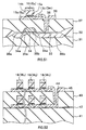
- Fig. 52 shows an example in which the memory device of the embodiment are formed in a stacked structure (two-layer structure in this case).
- a buffer layer 42 made of Si 3 N 4 SiO 2 is formed on a semiconductor substrate 41
- the memory device according to the embodiment is fabricated, and after that, by using CVD or sputtering, an interlayer insulating film 43 is formed by using SiO 2 , Si(OC 2 H 6 ) 4 (TEOS), or SOG (Spin On Glass).
- the surface of the interlayer insulating film 43 is planarized by CMP, and while the memory device in the second layer is fabricated, a contact hole 44 is opened in the interlayer insulating film 43, and a wiring 45 is formed by depositing a metal film made of Al, Cu, W, or the like.
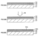
- an SiO 2 film 52 having a thickness of 200 nm was deposited on a glass substrate 51 by PECVD.
- a plastic substrate made of, for example, polyether sulfone (PES), polymethyl methacrylate (PMMA), or polyethylene terephthalate (PET), or a silicon wafer, or the like may be used.
- a Si film 53 having a thickness of 30 nm was deposited on the SiO 2 film 52 by PECVD.
- the Si film 53 may be in an amorphous state or a microcrystal state.
- an SiO x (x ⁇ 2) (silicon nitride) film 54 of a nonstoichiometric composition containing excessive Si was formed by PECVD using an SiH4 gas, having the flow rate of 20 SCCM, and an N2O gas, having the flow rate of 20 SCCM.
- the surface of the glass substrate 51 on which the SiO x film 54 was formed was irradiated with a laser beam 15 of 280 mJ/cm 2 having the pulse width of 10 to 50 nsec.
- a laser an excimer laser of KrF (resonant wavelength of 248 nm), ArF (resonant wavelength of 193 nm), XeCl (resonant wavelength of 308 nm) or the like may be used. In this case, the XeCl excimer laser was used.
- the SiO x film 54 was decomposed into SiO 2 and Si of the stoichiometric compositions. That is, more than one particulates 54b of Si was formed in a SiO 2 film 54a.
- the size of the particulate 54b lay within the range from 1 nm to 1 ⁇ m.
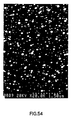
- Fig. 54 shows the result of an SEM (Scanning Electron Microscope) photograph after the irradiation of the energy beam and it is visible that white bright dots are scattered in a black region. Further, as a result of examination of the difference between the dark region, which is considered as SiO 2 , and the light region, which is considered as spread Si by micro AES (Auger Electron Spectroscopy), it was found that Si was concentrated in the light region more than the dark region.
- SEM Sccanning Electron Microscope
- the SiO x film 54 containing excessive Si was formed on the Si film 53 deposited on the glass substrate 51. Subsequently, heat treatment was performed by irradiating the SiO x film 54 with the laser beam 55, thereby enabling the storage region comprising many particulates 54b to be formed.
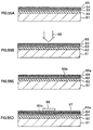
- a SiO 2 film 62 having a thickness of 200 nm was formed on a glass substrate 61 by PECVD.
- a Si film 63 for a memory channel having a thickness of 30 nm was formed on the SiO 2 film 62.
- an SiO 2 film 64 having a thickness of 1 nm to 10 nm was formed by PECVD.
- a SiO x (x ⁇ 2) film 65 containing excessive Si was formed by PECVD using the SiH 4 gas, having the flow rate of 20 SCCM, and the N 2 0 gas having the flow rate of 20 SCCM.
- the surface of the glass substrate 61 on which the SiO x film 65 was formed was irradiated with an excimer laser beam 66 of 280 mJ/cm 2 .
- the SiO x film 65 was decomposed into a SiO 2 film 65a and Si particulates 65b dispersed in the SiO 2 film 65a.
- the SiO 2 film 65a in which the particulates 65b are dispersed becomes a floating gate.
- a SiO 2 film 67 having a thickness of 100 nm was deposited on the SiO 2 film 65a by PECVD.
- a control gate 68 made of Ta (tantalum) having a film thickness of 100 nm was formed on the SiO 2 film 67. More specifically, the tantalum film was formed on the SiO 2 film 67 by, for example, sputtering, and after that, a photoresist film of a gate pattern was formed on the tantalum film, the tantalum film was etched using the photoresist film as a mask, and the photoresist film was peeled off, thereby forming the control gate 68.
- the SiO 2 film 67, the SiO 2 film 65 containing the particulates 65b, and the SiO 2 film 64 were sequentially selectively etched using the control gate 68 as a mask.
- an n-type impurity phosphorus (P) was introduced into the Si film 63 by plasma doping using plasma of PH 3 at a low temperature of 90 ° C using the control gate 68 as a mask.
- a first impurity region 63b and a second impurity region 63c were formed in a self-aligned manner on both sides of a conduction region 63a under the control gate 68. Then the surface of the substrate was irradiated with the excimer laser beam (wavelength 308 nm), thereby activating the impurities in the first impurity region 63b and the second impurity region 63c.
- an Si 3 N 4 film 69 as a protective film was formed on the surface of the substrate by, for example, PECVD, and after that contact holes for a source, a gate, and a drain are opened in the Si 3 N 4 film 69, aluminum (Al) was deposited by, for example, sputtering, and then patterning was performed, thereby forming a source electrode 70a, a gate electrode 70b, and a drain electrode 70c.
- the non-volatile memory device having the floating gate (storage region) in which Si particulates were contained was fabricated.
- the memory device when a large, positive bias with respect to the conduction region 63a is applied to the gate electrode 70b in a state, where a current is passed between the first and second impurity regions 63b and 63c, electrons tunneled the insulating film are stored in the Si dots 65b and the I-V characteristics are accordingly changed.
- a negative bias is applied to the gate electrode 60b, the electrons stored in the Si dots 65b tunnel the insulating film and are released into the conduction region 63a. As a result, the original I-V characteristics are obtained.
- the Si dots 65b in the gate insulating film As described above, the charges are stored or released and the memory effect can be produced.
- the structure has the same action as that of what is called a flash memory having a continuous Si floating gate. Since the floating gate are in the state of dots, the ratio of leakage and dissipation of the charges stored in each dot is low, enabling the memory unit to have an excellent holding performance.
- the invention has been described by the embodiments, the invention is not limited to the embodiments.
- the example in which the invention is applied to the manufacture of the silicon dot memory has been described as the embodiments, as long as the particulates (dots) of silicon are used, the invention can also be applied to manufacture of other various devices.
- the invention can be applied to a flash memory having the floating gate.
- Si dots of other semiconductors may also be formed.
- Ge germanium
- SiFe 2 and SiGe as Group IV compound semiconductors
- dots made of a Group II-VI compound semiconductor or a Group III-V compound semiconductor, or dots made of a metal (Au, Sb, Sn) may also be formed.
- Examples of forming dots using a Group II-VI compound semiconductor an example of forming ZnSe dots by irradiating ZnO to which Se is added (or stacked structure of ZnO/ZnSe/ZnO) with a laser beam, and an example of forming ZnTe dots by using Te (tellurium) in place of Se in the above example may be mentioned.
- Examples of forming dots by using a Group III-V compound semiconductor an example of forming GaN dots in Si 3 N 4 by irradiating SiNx to which Ga is added (or a stacked structure of Si 3 N 4 /GaN/Si 3 N 4 ) with a laser beam, and further an example of forming InAs dots in AlGaAs by irradiating a stacked structure of AlGaAs/InAs/AlGaAs with a laser beam may be mentioned.
- the surface density of the particulates in the storage region is set to be higher than the surface density of the structural holes (pin holes) produced in the tunnel insulating film or the number of particulates in the storage region is set to five or more.
- the conduction region is formed by the polysilicon film having the surface roughness of 0.1 nm to 10 nm
- the numberof particulates in the storage region is set to be larger than that of crystal grains in the conduction region. Accordingly the tunnel insulating film can be manufactured at a low temperature on the substrate made of glass or plastic.
- the heat treatment such as irradiation of an energy beam is performed to the film for forming the storage region of the nonstoichiometric composition containing a semiconductor excessively, so that the storage region having many dispersed particulates can be easily formed also on the substrate made of glass or plastic.
- the memory device according to the invention is suitable for use in a non-volatile storage device and a data processing apparatus.
Landscapes
- Engineering & Computer Science (AREA)
- Chemical & Material Sciences (AREA)
- Nanotechnology (AREA)
- Physics & Mathematics (AREA)
- Mathematical Physics (AREA)
- Theoretical Computer Science (AREA)
- Crystallography & Structural Chemistry (AREA)
- Semiconductor Memories (AREA)
- Non-Volatile Memory (AREA)
Applications Claiming Priority (5)
| Application Number | Priority Date | Filing Date | Title |
|---|---|---|---|
| JP2774798 | 1998-01-26 | ||
| JP2774798 | 1998-01-26 | ||
| JP32137798A JP4538693B2 (ja) | 1998-01-26 | 1998-10-28 | メモリ素子およびその製造方法 |
| JP32137798 | 1998-10-28 | ||
| PCT/JP1999/000313 WO1999038213A1 (en) | 1998-01-26 | 1999-01-26 | Memory device and method of manufacturing the same, and integrated circuit and method of manufacturing semiconductor device |
Publications (2)
| Publication Number | Publication Date |
|---|---|
| EP0971416A1 true EP0971416A1 (de) | 2000-01-12 |
| EP0971416A4 EP0971416A4 (de) | 2000-08-09 |
Family
ID=26365719
Family Applications (1)
| Application Number | Title | Priority Date | Filing Date |
|---|---|---|---|
| EP99901180A Withdrawn EP0971416A4 (de) | 1998-01-26 | 1999-01-26 | Speicheranordnung und verfahren zu deren herstellung, und integrierte schaltung und verfahren zur herstellung einer halbleiteranordnung |
Country Status (6)
| Country | Link |
|---|---|
| US (1) | US6285055B1 (de) |
| EP (1) | EP0971416A4 (de) |
| JP (1) | JP4538693B2 (de) |
| KR (1) | KR100638772B1 (de) |
| CN (2) | CN1169225C (de) |
| WO (1) | WO1999038213A1 (de) |
Cited By (9)
| Publication number | Priority date | Publication date | Assignee | Title |
|---|---|---|---|---|
| WO2001099167A3 (en) * | 2000-06-16 | 2002-04-04 | Motorola Inc | Memory device including nanoclusters and method for manufacture |
| US6413819B1 (en) | 2000-06-16 | 2002-07-02 | Motorola, Inc. | Memory device and method for using prefabricated isolated storage elements |
| EP1304730A3 (de) * | 2001-10-19 | 2007-10-10 | Chartered Semiconductor Manufacturing Ltd. | Nanokristall-FLASH-Speicherbauelement und dessen Herstellungsverfahren |
| FR2917533A1 (fr) * | 2007-11-14 | 2008-12-19 | Commissariat Energie Atomique | Substrat a couche de stockage de charges electriques enterree et procede de realisation |
| US7615436B2 (en) | 2001-03-28 | 2009-11-10 | Sandisk 3D Llc | Two mask floating gate EEPROM and method of making |
| US7825455B2 (en) | 2000-08-14 | 2010-11-02 | Sandisk 3D Llc | Three terminal nonvolatile memory device with vertical gated diode |
| US7868328B2 (en) | 2004-05-28 | 2011-01-11 | Semiconductor Energy Laboratory Co., Ltd. | Semiconductor device having antenna over thin film integrated circuit |
| US8258030B2 (en) | 2004-06-14 | 2012-09-04 | Semiconductor Energy Laboratory Co., Ltd. | Manufacturing method of semiconductor device |
| US9793276B2 (en) | 2010-02-05 | 2017-10-17 | Semiconductor Energy Laboratory Co., Ltd. | Semiconductor device having transistor and capacitor |
Families Citing this family (39)
| Publication number | Priority date | Publication date | Assignee | Title |
|---|---|---|---|---|
| US6452856B1 (en) * | 1999-02-26 | 2002-09-17 | Micron Technology, Inc. | DRAM technology compatible processor/memory chips |
| JP2001085545A (ja) * | 1999-09-16 | 2001-03-30 | Sony Corp | メモリ素子の製造方法 |
| TW587252B (en) | 2000-01-18 | 2004-05-11 | Hitachi Ltd | Semiconductor memory device and data processing device |
| JP2002050704A (ja) * | 2000-08-01 | 2002-02-15 | Sony Corp | メモリ素子およびその製造方法並びに集積回路 |
| JP2002050762A (ja) * | 2000-08-02 | 2002-02-15 | Sony Corp | 表示素子およびその製造方法、並びに表示装置 |
| JP2002368141A (ja) * | 2001-06-06 | 2002-12-20 | Sony Corp | 不揮発性半導体メモリ装置 |
| JP4670187B2 (ja) * | 2001-06-06 | 2011-04-13 | ソニー株式会社 | 不揮発性半導体メモリ装置 |
| CN100451831C (zh) * | 2001-10-29 | 2009-01-14 | 旺宏电子股份有限公司 | 减小图案间隙或开口尺寸的方法 |
| US6555411B1 (en) * | 2001-12-18 | 2003-04-29 | Lucent Technologies Inc. | Thin film transistors |
| JP3745297B2 (ja) | 2002-03-27 | 2006-02-15 | Necエレクトロニクス株式会社 | 不揮発性半導体記憶装置の製造方法 |
| US7005697B2 (en) * | 2002-06-21 | 2006-02-28 | Micron Technology, Inc. | Method of forming a non-volatile electron storage memory and the resulting device |
| US6853035B1 (en) * | 2002-06-28 | 2005-02-08 | Synopsys, Inc. | Negative differential resistance (NDR) memory device with reduced soft error rate |
| KR100486607B1 (ko) * | 2002-09-17 | 2005-05-03 | 주식회사 하이닉스반도체 | 양자점 형성 방법 |
| FR2846795A1 (fr) * | 2002-11-05 | 2004-05-07 | St Microelectronics Sa | Procede de memorisation d'une donnee binaire dans une cellule-memoire d'un circuit integre de memoire, circuit integre correspondant et procede de fabrication |
| US6905908B2 (en) * | 2002-12-26 | 2005-06-14 | Motorola, Inc. | Method of fabricating organic field effect transistors |
| US7022571B2 (en) * | 2003-05-01 | 2006-04-04 | United Microelectronics Corp. | Quantum structure and forming method of the same |
| US7057258B2 (en) * | 2003-10-29 | 2006-06-06 | Hewlett-Packard Development Company, L.P. | Resistive memory device and method for making the same |
| KR100537554B1 (ko) * | 2004-02-23 | 2005-12-16 | 주식회사 하이닉스반도체 | 반도체 소자의 산화막 형성 방법 |
| US7235471B2 (en) * | 2004-05-26 | 2007-06-26 | Freescale Semiconductor, Inc. | Method for forming a semiconductor device having a silicide layer |
| JP4942950B2 (ja) * | 2004-05-28 | 2012-05-30 | 株式会社半導体エネルギー研究所 | 半導体装置の作製方法 |
| TW200541079A (en) * | 2004-06-04 | 2005-12-16 | Adv Lcd Tech Dev Ct Co Ltd | Crystallizing method, thin-film transistor manufacturing method, thin-film transistor, and display device |
| JP4657016B2 (ja) * | 2004-06-14 | 2011-03-23 | 株式会社半導体エネルギー研究所 | 半導体装置の作製方法 |
| US7091089B2 (en) * | 2004-06-25 | 2006-08-15 | Freescale Semiconductor, Inc. | Method of forming a nanocluster charge storage device |
| US7977253B2 (en) * | 2004-08-31 | 2011-07-12 | Semiconductor Energy Laboratory Co., Ltd. | Manufacturing method of semiconductor device |
| JP5466815B2 (ja) * | 2006-03-31 | 2014-04-09 | 株式会社半導体エネルギー研究所 | 半導体装置 |
| JP2007287856A (ja) | 2006-04-14 | 2007-11-01 | Toshiba Corp | 半導体装置の製造方法 |
| KR100806788B1 (ko) | 2006-08-23 | 2008-02-27 | 동부일렉트로닉스 주식회사 | 플래시 메모리 소자 및 그 제조 방법 |
| KR101283539B1 (ko) * | 2007-08-29 | 2013-07-15 | 삼성전자주식회사 | 역전 구조의 비휘발성 메모리 소자, 그 스택 모듈 및 그제조 방법 |
| JP5134331B2 (ja) * | 2007-10-05 | 2013-01-30 | 株式会社東芝 | 半導体記憶装置およびその製造方法 |
| JP2011071240A (ja) * | 2009-09-24 | 2011-04-07 | Toshiba Corp | 半導体記憶装置、及びその製造方法 |
| WO2011058864A1 (en) * | 2009-11-13 | 2011-05-19 | Semiconductor Energy Laboratory Co., Ltd. | Device including nonvolatile memory element |
| JP2011233913A (ja) * | 2011-07-04 | 2011-11-17 | Getner Foundation Llc | 不揮発性記憶装置及びその製造方法 |
| JP5435129B2 (ja) * | 2011-10-26 | 2014-03-05 | トヨタ自動車株式会社 | 半導体装置 |
| US9093158B2 (en) * | 2013-12-06 | 2015-07-28 | Sandisk Technologies Inc. | Write scheme for charge trapping memory |
| US9627395B2 (en) | 2015-02-11 | 2017-04-18 | Sandisk Technologies Llc | Enhanced channel mobility three-dimensional memory structure and method of making thereof |
| US9478495B1 (en) | 2015-10-26 | 2016-10-25 | Sandisk Technologies Llc | Three dimensional memory device containing aluminum source contact via structure and method of making thereof |
| US10199434B1 (en) | 2018-02-05 | 2019-02-05 | Sandisk Technologies Llc | Three-dimensional cross rail phase change memory device and method of manufacturing the same |
| US10468596B2 (en) | 2018-02-21 | 2019-11-05 | Sandisk Technologies Llc | Damascene process for forming three-dimensional cross rail phase change memory devices |
| US10580976B2 (en) | 2018-03-19 | 2020-03-03 | Sandisk Technologies Llc | Three-dimensional phase change memory device having a laterally constricted element and method of making the same |
Family Cites Families (24)
| Publication number | Priority date | Publication date | Assignee | Title |
|---|---|---|---|---|
| GB1297899A (de) * | 1970-10-02 | 1972-11-29 | ||
| US4047974A (en) | 1975-12-30 | 1977-09-13 | Hughes Aircraft Company | Process for fabricating non-volatile field effect semiconductor memory structure utilizing implanted ions to induce trapping states |
| JPS5726469A (en) * | 1980-02-27 | 1982-02-12 | Tdk Corp | Semiconductor memory device |
| JPS6146058A (ja) * | 1984-08-10 | 1986-03-06 | Hitachi Ltd | 半導体装置およびその読み出し方法 |
| JPS6223173A (ja) * | 1985-07-23 | 1987-01-31 | Nec Corp | Mos型不揮発性半導体記憶装置 |
| US5017505A (en) * | 1986-07-18 | 1991-05-21 | Nippondenso Co., Ltd. | Method of making a nonvolatile semiconductor memory apparatus with a floating gate |
| CA2001682C (en) * | 1988-10-28 | 1994-05-03 | Hiroshi Matsumoto | Thin film transistor having memory function and method for using thin film transistor as memory element |
| JPH0821637B2 (ja) * | 1989-10-05 | 1996-03-04 | 工業技術院長 | 半導体記憶素子 |
| JPH0425181A (ja) * | 1990-05-21 | 1992-01-28 | Casio Comput Co Ltd | 薄膜トランジスタメモリおよびその製造方法 |
| JPH05121763A (ja) * | 1991-10-30 | 1993-05-18 | Rohm Co Ltd | 半導体記憶装置の製造方法 |
| US5357134A (en) | 1991-10-31 | 1994-10-18 | Rohm Co., Ltd. | Nonvolatile semiconductor device having charge trap film containing silicon crystal grains |
| JPH05211339A (ja) * | 1992-10-20 | 1993-08-20 | Casio Comput Co Ltd | 薄膜メモリ素子 |
| EP0655788B1 (de) * | 1993-11-29 | 1998-01-21 | STMicroelectronics S.A. | Flüchtige Speicherzelle |
| US5466626A (en) * | 1993-12-16 | 1995-11-14 | International Business Machines Corporation | Micro mask comprising agglomerated material |
| US5508543A (en) * | 1994-04-29 | 1996-04-16 | International Business Machines Corporation | Low voltage memory |
| US5828084A (en) | 1995-03-27 | 1998-10-27 | Sony Corporation | High performance poly-SiGe thin film transistor |
| JP3306258B2 (ja) * | 1995-03-27 | 2002-07-24 | 三洋電機株式会社 | 半導体装置の製造方法 |
| JPH0969630A (ja) * | 1995-06-23 | 1997-03-11 | Matsushita Electric Ind Co Ltd | 単一電子トンネル素子およびその製造方法 |
| US5714766A (en) * | 1995-09-29 | 1998-02-03 | International Business Machines Corporation | Nano-structure memory device |
| JPH09102596A (ja) * | 1995-10-04 | 1997-04-15 | Fujitsu Ltd | 量子ドットの製造方法及び量子ドット装置 |
| JPH09260611A (ja) * | 1996-03-19 | 1997-10-03 | Toshiba Corp | 電子デバイス |
| JPH1065024A (ja) * | 1996-08-13 | 1998-03-06 | Toshiba Corp | 不揮発性半導体記憶装置 |
| DE19632834C2 (de) * | 1996-08-14 | 1998-11-05 | Siemens Ag | Verfahren zur Herstellung feiner Strukturen und dessen Verwendung zur Herstellung einer Maske und eines MOS-Transistors |
| US5880991A (en) * | 1997-04-14 | 1999-03-09 | International Business Machines Corporation | Structure for low cost mixed memory integration, new NVRAM structure, and process for forming the mixed memory and NVRAM structure |
-
1998
- 1998-10-28 JP JP32137798A patent/JP4538693B2/ja not_active Expired - Fee Related
-
1999
- 1999-01-26 WO PCT/JP1999/000313 patent/WO1999038213A1/ja not_active Ceased
- 1999-01-26 EP EP99901180A patent/EP0971416A4/de not_active Withdrawn
- 1999-01-26 CN CNB998001775A patent/CN1169225C/zh not_active Expired - Fee Related
- 1999-01-26 CN CNB2004100328296A patent/CN1309087C/zh not_active Expired - Fee Related
- 1999-01-26 US US09/381,987 patent/US6285055B1/en not_active Expired - Lifetime
- 1999-01-26 KR KR1019997008723A patent/KR100638772B1/ko not_active Expired - Fee Related
Cited By (12)
| Publication number | Priority date | Publication date | Assignee | Title |
|---|---|---|---|---|
| WO2001099167A3 (en) * | 2000-06-16 | 2002-04-04 | Motorola Inc | Memory device including nanoclusters and method for manufacture |
| US6413819B1 (en) | 2000-06-16 | 2002-07-02 | Motorola, Inc. | Memory device and method for using prefabricated isolated storage elements |
| US7825455B2 (en) | 2000-08-14 | 2010-11-02 | Sandisk 3D Llc | Three terminal nonvolatile memory device with vertical gated diode |
| US8981457B2 (en) | 2000-08-14 | 2015-03-17 | Sandisk 3D Llc | Dense arrays and charge storage devices |
| US10008511B2 (en) | 2000-08-14 | 2018-06-26 | Sandisk Technologies Llc | Dense arrays and charge storage devices |
| US10644021B2 (en) | 2000-08-14 | 2020-05-05 | Sandisk Technologies Llc | Dense arrays and charge storage devices |
| US7615436B2 (en) | 2001-03-28 | 2009-11-10 | Sandisk 3D Llc | Two mask floating gate EEPROM and method of making |
| EP1304730A3 (de) * | 2001-10-19 | 2007-10-10 | Chartered Semiconductor Manufacturing Ltd. | Nanokristall-FLASH-Speicherbauelement und dessen Herstellungsverfahren |
| US7868328B2 (en) | 2004-05-28 | 2011-01-11 | Semiconductor Energy Laboratory Co., Ltd. | Semiconductor device having antenna over thin film integrated circuit |
| US8258030B2 (en) | 2004-06-14 | 2012-09-04 | Semiconductor Energy Laboratory Co., Ltd. | Manufacturing method of semiconductor device |
| FR2917533A1 (fr) * | 2007-11-14 | 2008-12-19 | Commissariat Energie Atomique | Substrat a couche de stockage de charges electriques enterree et procede de realisation |
| US9793276B2 (en) | 2010-02-05 | 2017-10-17 | Semiconductor Energy Laboratory Co., Ltd. | Semiconductor device having transistor and capacitor |
Also Published As
| Publication number | Publication date |
|---|---|
| JP4538693B2 (ja) | 2010-09-08 |
| EP0971416A4 (de) | 2000-08-09 |
| KR20010005655A (ko) | 2001-01-15 |
| WO1999038213A1 (en) | 1999-07-29 |
| CN1542976A (zh) | 2004-11-03 |
| CN1256793A (zh) | 2000-06-14 |
| KR100638772B1 (ko) | 2006-10-27 |
| CN1309087C (zh) | 2007-04-04 |
| JPH11274420A (ja) | 1999-10-08 |
| CN1169225C (zh) | 2004-09-29 |
| US6285055B1 (en) | 2001-09-04 |
Similar Documents
| Publication | Publication Date | Title |
|---|---|---|
| EP0971416A1 (de) | Speicheranordnung und verfahren zu deren herstellung, und integrierte schaltung und verfahren zur herstellung einer halbleiteranordnung | |
| US5847411A (en) | Semiconductor device having a channel region including a vacancy-introduced polysilicon layer | |
| US6677204B2 (en) | Multigate semiconductor device with vertical channel current and method of fabrication | |
| US6548830B1 (en) | Semiconductor device formed of single crystal grains in a grid pattern | |
| US4115914A (en) | Electrically erasable non-volatile semiconductor memory | |
| US7663176B2 (en) | Method of manufacturing a nonvolatile semiconductor memory device, and a nonvolatile semiconductor memory device | |
| US7485527B2 (en) | Nonvolatile semiconductor storage device and its manufacturing method | |
| US5814543A (en) | Method of manufacturing a semicondutor integrated circuit device having nonvolatile memory cells | |
| US6410412B1 (en) | Methods for fabricating memory devices | |
| US6525379B2 (en) | Memory device, method of manufacturing the same, and integrated circuit | |
| JP4026191B2 (ja) | シリコン単結晶粒子群の形成方法及びフラッシュメモリセルの製造方法 | |
| US6274903B1 (en) | Memory device having a storage region is constructed with a plurality of dispersed particulates | |
| KR0161721B1 (ko) | 반도체 기억장치와 그 제조방법 | |
| JP2002289708A (ja) | 不揮発性半導体記憶装置およびその製造方法 | |
| CN100524633C (zh) | 半导体装置的制造方法 | |
| JP4059299B2 (ja) | シリコン薄膜、シリコン単結晶粒子群、半導体装置、及び、フラッシュメモリセル | |
| US6897506B2 (en) | Systems and methods using non-volatile memory cells | |
| US10164061B2 (en) | Method of fabricating non-volatile memory device array | |
| KR100782911B1 (ko) | 나노결정을 균일하게 형성하는 방법 및 나노결정을포함하는 소자 | |
| Walker | Sub-50nm DG-TFT-SONOS-the ideal Flash memory for monolithic 3-D integration | |
| JP4224000B2 (ja) | 半導体装置の製造方法 | |
| CN121773718A (zh) | 包括具有超晶格的耗尽层的非易失性存储器和相关方法 | |
| WO2007140081A2 (en) | Dual-gate semiconductor devices with enhance scalability |
Legal Events
| Date | Code | Title | Description |
|---|---|---|---|
| PUAI | Public reference made under article 153(3) epc to a published international application that has entered the european phase |
Free format text: ORIGINAL CODE: 0009012 |
|
| 17P | Request for examination filed |
Effective date: 19991025 |
|
| AK | Designated contracting states |
Kind code of ref document: A1 Designated state(s): DE FR GB |
|
| A4 | Supplementary search report drawn up and despatched |
Effective date: 20000627 |
|
| AK | Designated contracting states |
Kind code of ref document: A4 Designated state(s): DE FR GB |
|
| RIC1 | Information provided on ipc code assigned before grant |
Free format text: 7H 01L 27/115 A, 7H 01L 21/8247 B, 7H 01L 29/788 B, 7H 01L 29/792 B, 7H 01L 21/336 B, 7H 01L 27/12 B |
|
| 17Q | First examination report despatched |
Effective date: 20010628 |
|
| 17Q | First examination report despatched |
Effective date: 20010628 |
|
| STAA | Information on the status of an ep patent application or granted ep patent |
Free format text: STATUS: THE APPLICATION IS DEEMED TO BE WITHDRAWN |
|
| 18D | Application deemed to be withdrawn |
Effective date: 20091201 |