EP0973192A2 - Verfahren und Vorrichtung zum Verarbeiten eines in Harz versiegelten Leiterrahmens - Google Patents
Verfahren und Vorrichtung zum Verarbeiten eines in Harz versiegelten Leiterrahmens Download PDFInfo
- Publication number
- EP0973192A2 EP0973192A2 EP99305444A EP99305444A EP0973192A2 EP 0973192 A2 EP0973192 A2 EP 0973192A2 EP 99305444 A EP99305444 A EP 99305444A EP 99305444 A EP99305444 A EP 99305444A EP 0973192 A2 EP0973192 A2 EP 0973192A2
- Authority
- EP
- European Patent Office
- Prior art keywords
- processing
- lead frame
- resin sealed
- lead
- sealed lead
- Prior art date
- Legal status (The legal status is an assumption and is not a legal conclusion. Google has not performed a legal analysis and makes no representation as to the accuracy of the status listed.)
- Withdrawn
Links
Images




Classifications
-
- H—ELECTRICITY
- H10—SEMICONDUCTOR DEVICES; ELECTRIC SOLID-STATE DEVICES NOT OTHERWISE PROVIDED FOR
- H10W—GENERIC PACKAGES, INTERCONNECTIONS, CONNECTORS OR OTHER CONSTRUCTIONAL DETAILS OF DEVICES COVERED BY CLASS H10
- H10W99/00—Subject matter not provided for in other groups of this subclass
-
- H—ELECTRICITY
- H10—SEMICONDUCTOR DEVICES; ELECTRIC SOLID-STATE DEVICES NOT OTHERWISE PROVIDED FOR
- H10W—GENERIC PACKAGES, INTERCONNECTIONS, CONNECTORS OR OTHER CONSTRUCTIONAL DETAILS OF DEVICES COVERED BY CLASS H10
- H10W70/00—Package substrates; Interposers; Redistribution layers [RDL]
- H10W70/01—Manufacture or treatment
- H10W70/04—Manufacture or treatment of leadframes
- H10W70/048—Mechanical treatments, e.g. punching, cutting, deforming or cold welding
-
- H—ELECTRICITY
- H10—SEMICONDUCTOR DEVICES; ELECTRIC SOLID-STATE DEVICES NOT OTHERWISE PROVIDED FOR
- H10W—GENERIC PACKAGES, INTERCONNECTIONS, CONNECTORS OR OTHER CONSTRUCTIONAL DETAILS OF DEVICES COVERED BY CLASS H10
- H10W72/00—Interconnections or connectors in packages
- H10W72/01—Manufacture or treatment
- H10W72/0198—Manufacture or treatment batch processes
-
- H—ELECTRICITY
- H10—SEMICONDUCTOR DEVICES; ELECTRIC SOLID-STATE DEVICES NOT OTHERWISE PROVIDED FOR
- H10W—GENERIC PACKAGES, INTERCONNECTIONS, CONNECTORS OR OTHER CONSTRUCTIONAL DETAILS OF DEVICES COVERED BY CLASS H10
- H10W74/00—Encapsulations, e.g. protective coatings
- H10W74/01—Manufacture or treatment
-
- H—ELECTRICITY
- H10—SEMICONDUCTOR DEVICES; ELECTRIC SOLID-STATE DEVICES NOT OTHERWISE PROVIDED FOR
- H10W—GENERIC PACKAGES, INTERCONNECTIONS, CONNECTORS OR OTHER CONSTRUCTIONAL DETAILS OF DEVICES COVERED BY CLASS H10
- H10W72/00—Interconnections or connectors in packages
- H10W72/50—Bond wires
- H10W72/541—Dispositions of bond wires
- H10W72/5449—Dispositions of bond wires not being orthogonal to a side surface of the chip, e.g. fan-out arrangements
-
- H—ELECTRICITY
- H10—SEMICONDUCTOR DEVICES; ELECTRIC SOLID-STATE DEVICES NOT OTHERWISE PROVIDED FOR
- H10W—GENERIC PACKAGES, INTERCONNECTIONS, CONNECTORS OR OTHER CONSTRUCTIONAL DETAILS OF DEVICES COVERED BY CLASS H10
- H10W74/00—Encapsulations, e.g. protective coatings
-
- H—ELECTRICITY
- H10—SEMICONDUCTOR DEVICES; ELECTRIC SOLID-STATE DEVICES NOT OTHERWISE PROVIDED FOR
- H10W—GENERIC PACKAGES, INTERCONNECTIONS, CONNECTORS OR OTHER CONSTRUCTIONAL DETAILS OF DEVICES COVERED BY CLASS H10
- H10W90/00—Package configurations
- H10W90/701—Package configurations characterised by the relative positions of pads or connectors relative to package parts
- H10W90/751—Package configurations characterised by the relative positions of pads or connectors relative to package parts of bond wires
- H10W90/756—Package configurations characterised by the relative positions of pads or connectors relative to package parts of bond wires between a chip and a stacked lead frame, conducting package substrate or heat sink
-
- Y—GENERAL TAGGING OF NEW TECHNOLOGICAL DEVELOPMENTS; GENERAL TAGGING OF CROSS-SECTIONAL TECHNOLOGIES SPANNING OVER SEVERAL SECTIONS OF THE IPC; TECHNICAL SUBJECTS COVERED BY FORMER USPC CROSS-REFERENCE ART COLLECTIONS [XRACs] AND DIGESTS
- Y10—TECHNICAL SUBJECTS COVERED BY FORMER USPC
- Y10S—TECHNICAL SUBJECTS COVERED BY FORMER USPC CROSS-REFERENCE ART COLLECTIONS [XRACs] AND DIGESTS
- Y10S438/00—Semiconductor device manufacturing: process
- Y10S438/907—Continuous processing
-
- Y—GENERAL TAGGING OF NEW TECHNOLOGICAL DEVELOPMENTS; GENERAL TAGGING OF CROSS-SECTIONAL TECHNOLOGIES SPANNING OVER SEVERAL SECTIONS OF THE IPC; TECHNICAL SUBJECTS COVERED BY FORMER USPC CROSS-REFERENCE ART COLLECTIONS [XRACs] AND DIGESTS
- Y10—TECHNICAL SUBJECTS COVERED BY FORMER USPC
- Y10S—TECHNICAL SUBJECTS COVERED BY FORMER USPC CROSS-REFERENCE ART COLLECTIONS [XRACs] AND DIGESTS
- Y10S438/00—Semiconductor device manufacturing: process
- Y10S438/907—Continuous processing
- Y10S438/908—Utilizing cluster apparatus
Definitions
- a step of cutting and separating the works on the resin sealed lead frame can be further provided before removal of the resin sealed lead frame from the removing portion.
- the lead processing step is not performed.
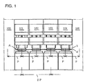
- the resin sealed lead frame may be fed by four pitches (see first portion 13a shown in Figs. 9B(b) and (d)). Further, to feed from additional lead processing basic unit 310 to removing portion 32 or from additional lead processing basic unit 310 to work cutting and separating portion (D1, D2), the resin sealed lead frame may be similarly fed by four pitches.
Landscapes
- Encapsulation Of And Coatings For Semiconductor Or Solid State Devices (AREA)
- Lead Frames For Integrated Circuits (AREA)
Applications Claiming Priority (4)
| Application Number | Priority Date | Filing Date | Title |
|---|---|---|---|
| JP21961398 | 1998-07-17 | ||
| JP10219613A JP2000036555A (ja) | 1998-07-17 | 1998-07-17 | 樹脂封止済リードフレームの加工方法及び装置 |
| JP33111798 | 1998-11-20 | ||
| JP10331117A JP2000156449A (ja) | 1998-11-20 | 1998-11-20 | 樹脂封止済リードフレームの加工方法及び装置 |
Publications (2)
| Publication Number | Publication Date |
|---|---|
| EP0973192A2 true EP0973192A2 (de) | 2000-01-19 |
| EP0973192A3 EP0973192A3 (de) | 2002-05-08 |
Family
ID=26523241
Family Applications (1)
| Application Number | Title | Priority Date | Filing Date |
|---|---|---|---|
| EP99305444A Withdrawn EP0973192A3 (de) | 1998-07-17 | 1999-07-08 | Verfahren und Vorrichtung zum Verarbeiten eines in Harz versiegelten Leiterrahmens |
Country Status (6)
| Country | Link |
|---|---|
| US (2) | US6258628B1 (de) |
| EP (1) | EP0973192A3 (de) |
| KR (1) | KR100345262B1 (de) |
| MY (1) | MY120818A (de) |
| SG (1) | SG82620A1 (de) |
| TW (1) | TW486797B (de) |
Cited By (1)
| Publication number | Priority date | Publication date | Assignee | Title |
|---|---|---|---|---|
| NL1018510C2 (nl) * | 2001-07-11 | 2003-01-14 | Fico Bv | Werkwijze en inrichting voor het bewerken van een band met elektronische componenten en band met elektronische componenten. |
Families Citing this family (2)
| Publication number | Priority date | Publication date | Assignee | Title |
|---|---|---|---|---|
| SG82620A1 (en) * | 1998-07-17 | 2001-08-21 | Towa Corp | Method and apparatus for processing resin sealed lead frame |
| JP4079874B2 (ja) * | 2003-12-25 | 2008-04-23 | 沖電気工業株式会社 | 半導体装置の製造方法 |
Family Cites Families (7)
| Publication number | Priority date | Publication date | Assignee | Title |
|---|---|---|---|---|
| JPS6074552A (ja) * | 1983-09-30 | 1985-04-26 | Fujitsu Ltd | ダムリ−ド切断方法及び切断装置 |
| US4972572A (en) * | 1985-11-13 | 1990-11-27 | Fujitsu Limited | IC sheet cutting press and IC sheet processing apparatus using the same |
| NL9001999A (nl) * | 1990-09-11 | 1992-04-01 | Asm Fico Tooling | Stelsel van bewerkingsinrichtingen. |
| JP3174115B2 (ja) | 1991-12-20 | 2001-06-11 | 株式会社放電精密加工研究所 | 順送り加工装置用カセット交換装置 |
| US5332405A (en) * | 1992-09-01 | 1994-07-26 | Golomb Mark S | Apparatus for manufacturing semiconductor lead frames in a circular path |
| JP2790085B2 (ja) * | 1995-07-26 | 1998-08-27 | 日本電気株式会社 | 半導体装置の製造方法及び製造装置 |
| SG82620A1 (en) * | 1998-07-17 | 2001-08-21 | Towa Corp | Method and apparatus for processing resin sealed lead frame |
-
1999
- 1999-07-02 SG SG9903152A patent/SG82620A1/en unknown
- 1999-07-06 MY MYPI99002825A patent/MY120818A/en unknown
- 1999-07-08 EP EP99305444A patent/EP0973192A3/de not_active Withdrawn
- 1999-07-13 US US09/353,302 patent/US6258628B1/en not_active Expired - Fee Related
- 1999-07-15 TW TW088111994A patent/TW486797B/zh not_active IP Right Cessation
- 1999-07-16 KR KR1019990028975A patent/KR100345262B1/ko not_active Expired - Fee Related
-
2001
- 2001-05-08 US US09/851,227 patent/US20010021409A1/en not_active Abandoned
Cited By (2)
| Publication number | Priority date | Publication date | Assignee | Title |
|---|---|---|---|---|
| NL1018510C2 (nl) * | 2001-07-11 | 2003-01-14 | Fico Bv | Werkwijze en inrichting voor het bewerken van een band met elektronische componenten en band met elektronische componenten. |
| WO2003007673A1 (en) * | 2001-07-11 | 2003-01-23 | Fico B.V. | Method and apparatus for processing a strip with electronic components, and belt with electronic components |
Also Published As
| Publication number | Publication date |
|---|---|
| MY120818A (en) | 2005-11-30 |
| EP0973192A3 (de) | 2002-05-08 |
| KR100345262B1 (ko) | 2002-07-19 |
| TW486797B (en) | 2002-05-11 |
| US6258628B1 (en) | 2001-07-10 |
| US20010021409A1 (en) | 2001-09-13 |
| KR20000011794A (ko) | 2000-02-25 |
| SG82620A1 (en) | 2001-08-21 |
Similar Documents
| Publication | Publication Date | Title |
|---|---|---|
| US7943424B1 (en) | Encapsulation method for packaging semiconductor components with external leads | |
| EP0973192A2 (de) | Verfahren und Vorrichtung zum Verarbeiten eines in Harz versiegelten Leiterrahmens | |
| US5332405A (en) | Apparatus for manufacturing semiconductor lead frames in a circular path | |
| KR100335790B1 (ko) | 전자기기에사용되는컨택트제조방법,동방법을위한제조장치및동방법에사용되는연속띠재료 | |
| JP3175504B2 (ja) | リードフレームの製造方法および製造装置 | |
| JP2000036555A (ja) | 樹脂封止済リードフレームの加工方法及び装置 | |
| JP2000156449A (ja) | 樹脂封止済リードフレームの加工方法及び装置 | |
| JPH05185153A (ja) | 金型装置 | |
| US6269723B1 (en) | Method and apparatus for enhancement of a punch guide/receptor tool in a dambar removal system | |
| JP2559640B2 (ja) | 金型装置およびこれを用いたリードフレームの製造方法 | |
| KR101141704B1 (ko) | 리드 프레임의 제조방법 및 이에 적용되는 리드 프레임용프레스 가공장치 | |
| KR0123314Y1 (ko) | 반도체 제조장비에 있어서의 더블 포밍장치 | |
| KR20010026350A (ko) | "l"형 펀치를 이용한 칩 스케일 패키지 분리 방법 | |
| JPH03181160A (ja) | 半導体装置用リードフレーム | |
| JP2001179693A (ja) | 電子部品用フイルムの孔明け加工方法 | |
| KR200221823Y1 (ko) | 반도체 패키지 제조장비의 트림다이 | |
| JPH0940167A (ja) | 半導体装置の製造方法及び製造装置 | |
| KR100189822B1 (ko) | 금형용 펀치 연삭 가공방법 | |
| JPH04206558A (ja) | リード切断成形装置 | |
| JPS6358844A (ja) | リ−ドフレ−ムの送り方法 | |
| JPH07142659A (ja) | 電子部品用リードフレームの切断装置 | |
| JPH03181156A (ja) | リードフレームの製造方法 | |
| JPS6110262A (ja) | 半導体リ−ドフレ−ム製造装置 | |
| JP2007512206A (ja) | 電子部品を載せた担体を処理するための装置の製品関連調整を行うデバイスおよび方法 | |
| JPS6381963A (ja) | プレス成形機 |
Legal Events
| Date | Code | Title | Description |
|---|---|---|---|
| PUAI | Public reference made under article 153(3) epc to a published international application that has entered the european phase |
Free format text: ORIGINAL CODE: 0009012 |
|
| AK | Designated contracting states |
Kind code of ref document: A2 Designated state(s): AT BE CH CY DE DK ES FI FR GB GR IE IT LI LU MC NL PT SE |
|
| AX | Request for extension of the european patent |
Free format text: AL;LT;LV;MK;RO;SI |
|
| PUAL | Search report despatched |
Free format text: ORIGINAL CODE: 0009013 |
|
| AK | Designated contracting states |
Kind code of ref document: A3 Designated state(s): AT BE CH CY DE DK ES FI FR GB GR IE IT LI LU MC NL PT SE |
|
| AX | Request for extension of the european patent |
Free format text: AL;LT;LV;MK;RO;SI |
|
| RIC1 | Information provided on ipc code assigned before grant |
Free format text: 7H 01L 21/48 A, 7H 01L 21/00 B |
|
| 17P | Request for examination filed |
Effective date: 20020808 |
|
| AKX | Designation fees paid |
Designated state(s): DE GB NL |
|
| 17Q | First examination report despatched |
Effective date: 20030729 |
|
| GRAP | Despatch of communication of intention to grant a patent |
Free format text: ORIGINAL CODE: EPIDOSNIGR1 |
|
| GRAS | Grant fee paid |
Free format text: ORIGINAL CODE: EPIDOSNIGR3 |
|
| RAP1 | Party data changed (applicant data changed or rights of an application transferred) |
Owner name: TOWA CORPORATION |
|
| RIN1 | Information on inventor provided before grant (corrected) |
Inventor name: HORIUCHI, KAZUO,TOWA CORPORATION Inventor name: HIDAKA, TETSUO,TOWA CORPORATION Inventor name: OSADA, MICHIO,TOWA CORPORATION |
|
| STAA | Information on the status of an ep patent application or granted ep patent |
Free format text: STATUS: THE APPLICATION IS DEEMED TO BE WITHDRAWN |
|
| 18D | Application deemed to be withdrawn |
Effective date: 20050802 |