EP1003206B1 - Rutil-Dielektrikum für Halbleiter-Bauelement - Google Patents
Rutil-Dielektrikum für Halbleiter-Bauelement Download PDFInfo
- Publication number
- EP1003206B1 EP1003206B1 EP99119456A EP99119456A EP1003206B1 EP 1003206 B1 EP1003206 B1 EP 1003206B1 EP 99119456 A EP99119456 A EP 99119456A EP 99119456 A EP99119456 A EP 99119456A EP 1003206 B1 EP1003206 B1 EP 1003206B1
- Authority
- EP
- European Patent Office
- Prior art keywords
- layer
- trench
- barrier layer
- recited
- forming
- Prior art date
- Legal status (The legal status is an assumption and is not a legal conclusion. Google has not performed a legal analysis and makes no representation as to the accuracy of the status listed.)
- Expired - Lifetime
Links
Images


Classifications
-
- H—ELECTRICITY
- H10—SEMICONDUCTOR DEVICES; ELECTRIC SOLID-STATE DEVICES NOT OTHERWISE PROVIDED FOR
- H10D—INORGANIC ELECTRIC SEMICONDUCTOR DEVICES
- H10D84/00—Integrated devices formed in or on semiconductor substrates that comprise only semiconducting layers, e.g. on Si wafers or on GaAs-on-Si wafers
- H10D84/01—Manufacture or treatment
- H10D84/02—Manufacture or treatment characterised by using material-based technologies
-
- H—ELECTRICITY
- H10—SEMICONDUCTOR DEVICES; ELECTRIC SOLID-STATE DEVICES NOT OTHERWISE PROVIDED FOR
- H10B—ELECTRONIC MEMORY DEVICES
- H10B12/00—Dynamic random access memory [DRAM] devices
- H10B12/01—Manufacture or treatment
- H10B12/02—Manufacture or treatment for one transistor one-capacitor [1T-1C] memory cells
- H10B12/03—Making the capacitor or connections thereto
- H10B12/038—Making the capacitor or connections thereto the capacitor being in a trench in the substrate
-
- H—ELECTRICITY
- H10—SEMICONDUCTOR DEVICES; ELECTRIC SOLID-STATE DEVICES NOT OTHERWISE PROVIDED FOR
- H10D—INORGANIC ELECTRIC SEMICONDUCTOR DEVICES
- H10D1/00—Resistors, capacitors or inductors
- H10D1/01—Manufacture or treatment
- H10D1/045—Manufacture or treatment of capacitors having potential barriers, e.g. varactors
- H10D1/047—Manufacture or treatment of capacitors having potential barriers, e.g. varactors of conductor-insulator-semiconductor capacitors, e.g. trench capacitors
Definitions
- This invention relates to semiconductor devices and more particularly, to an improved dielectric layer and method of formation thereof.
- Semiconductor memory cells include capacitors accessed by transistors to store data. Data is stored as a high or low bit depending on the state of the capacitor. The capacitor's charge or lack of charge indicates a high or low when accessed to read data, and the capacitor is charged or discharged to write data thereto.
- Deep trench (DT) capacitors are among the types of capacitors used in semiconductor memories. Deep trench capacitors are typically buried within a semiconductor substrate of the device adjacent to or below an access transistor.
- the capacitance C of the storage trench capacitor should be maximized while the charge leakage to areas surrounding the capacitor should be minimized. These requirements dictate the use of high quality dielectric materials interposed between the plates of the capacitor.
- Oxinitride In conventional trench capacitor fabrication, an Oxinitride is typically used as the dielectric material. Oxinitride materials are highly compatible with current deep trench capacitor manufacturing processes and materials and are stable over the high temperature treatments incurred during the formation of deep trench capacitors (up to 1100° C). However, Oxinitrides typically exhibit a dielectric constant of about 7, which is insufficient to achieve the required capacitances without changing the geometry of the capacitor in a manner that degrades the leakage characteristics of the capacitor.
- TiO 2 has been described in IBM TDB, Vol. 32, No. 4b, pp. 343-344 , as a suitable dielectric material for a capacitor with a dielectric constant between 80 and 180 depending on the crystallographic axis.
- An anneal is necessary for reoxidizing the reduced TiO 2 into a good insulator growing an undesired layer of SiO 2 under the TiO 2 . This oxide layer reduces device capacitance due to the series capacitance formed.
- this objective can be obtained by using a dielectric material having a higher dielectric constant ⁇ which is compatible with the formation process of deep trench capacitors.
- a method of forming semiconductor devices in accordance with the present invention includes the steps of providing a deep trench in a substrate, the deep trench having a lower portion, annealing the substrate to remove native oxides from the surface of the trench, forming a first barrier layer in the deep trench after annealing by lining the deep trench, wherein the first barrier layer is a silicon nitride layer and is less than about 1nm in thickness, forming, on said first barrier layer, a dielectric layer in the deep trench by lining the deep trench, the dielectric layer including titanium dioxide in the rutile crystal form, filling a portion of the deep trench with a conductive filler material thereby forming a storage node and removing a portion of the first barrier layer and the dielectric layer such that the dielectric layer and the barrier layer line the lower portion of the deep trench.
- the step of forming the dielectric may include depositing rutile (TiO 2 ) by a chemical vapor deposition process.
- the step of providing a precursor material prior to depositing rutile (TiO 2 ) may also be included.
- the step of forming the dielectric layer may include forming the dielectric layer by depositing a layer of TiN in the lower portion of the deep trench and oxidizing the layer of TiN to form rutile (TiO 2 ).
- the step of oxidizing may further include the step of oxidizing the layer of TiN by plasma oxidation.
- the step of oxidizing may include the step of oxidizing the layer of TiN by rapid thermal oxidation.
- a semiconductor device includes a substrate having a trench formed therein, a conductive filler material forming a storage node, filling a portion of the trench and capacitively coupled to the substrate, a barrier layer in the trench between the conductive filler material and the substrate, the barrier layer lining a lower portion of the trench; wherein said barrier layer is a silicon nitride layer and is less than about 1 nm in thickness, and a dielectric layer in the trench between the conductive filler material and the said barrier layer and lining a lower portion of the trench,wherein the dielectric layer includes titanium oxide in the rutile crystal form.
- the titanium oxide layer is preferably between about 15 nanometers to about 35 nanometers in thickness.
- the present invention relates to semiconductor devices and more particularly, to an improved dielectric layer and method of formation thereof.
- the capacitance of a storage cell capacitor is important for the performance of dynamic random access memory (DRAM) devices.
- DRAM dynamic random access memory
- nitride is used as a dielectric in deep trench (DT) technology.
- the dielectric constant, ⁇ , of nitride is about 7.
- a nitride dielectric thickness d is already approaching its minimum limit of 3.5 nm which is within the tunneling regime.
- An adjustment of the DT capacitance towards the minimum critical value of about 40fF/cell becomes increasingly more difficult to achieve using the conventional process.
- the present invention describes an apparatus and method which uses rutile as the dielectric material.
- the dielectric constant of rutile is between about 86 for a crystal orientation with an optical axis (c-axis) perpendicular to a surface and 170 for the c-axis parallel to the surface. Consequently, an increase in the capacitance of at least an order of magnitude is realized if similar node thicknesses are used.
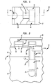
- FIGS. 1 and 2 show a fabricated deep trench capacitor 10.
- a semiconductor substrate 12 includes a trench (deep trench) 14 formed therein.
- Substrate 12 includes a well region 16 and a buried capacitor plate 18.
- Buried plate 18 is capacitively coupled to a storage node 20 formed within trench 14.
- Storage node 20 includes a conductive material, for example polycrystalline silicon (poly silicon).
- a lower portion 24 of trench 14 is lined with rutile to form a dielectric layer 26 between the buried capacitor plate 18 and the storage node 20.
- Storage node 20 is electrically coupled by a buried strap 28 to an access transistor 30.
- Access transistor includes a gate 32 preferably formed from a silicon oxide and contacted by a metal silicide, such as tungsten silicide, and/or poly silicon. When gate 32 is activated, charge flows between diffusion regions 34 and 36 thereby permitting charge to flow to and from a bitline 38 through a bitline contact 40.
- Storage node 20 is electrically isolated from well region 16 by a collar 42 formed in trench 14. Collar 42 preferably includes a silicon oxide. Storage node 20 is also isolated from a passing wordline gate 44 by shallow trench isolation 46. Gates 32 and 44 preferably extend along a semiconductor chip and form wordlines as shown in FIG. 1 .
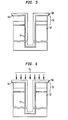
- Trench 14 etching is performed preferably using reactive ion etching (RIE).
- Trench 14 depth may be between about 2 to 10 micrometres.
- a top down shape of trench 14 may be round to oval and may range in diameters between about 50 and 400 nm.
- substrate 12 is oxidized to form a pad oxide layer 48 (silicon dioxide) about 5 nm in thickness.
- a pad nitride layer 50 (silicon nitride) is deposited over pad oxide layer 48.
- Pad nitride layer 50 may be about 200 nm to about 240 nm in thickness.
- a glass layer 52 for example borosilicate glass (BSG) is formed on pad nitride layer 50.
- Glass layer 52 may be about 700 nm in thickness. It is noted the above dimensions and materials are not critical and can be varied as needed.
- Pad oxide 48, pad nitride 50 and glass layer 52 are collectively referred to as a pad stack 54.
- Pad stack 54 is patterned according to known processes, such as by photolithography methods. Holes at locations where trenches 14 are to be formed are fabricated wherein the remaining portions of pad stack 54 act as a hard mask for RIE which follows to form the deep trenches.
- trench sidewall doping it is preferable to employ trench sidewall doping to form the buried capacitor plate 18.
- Different processes may be used to perform this doping for example, arsenic glass (ASG) deposition with subsequent drive-in of arsenic atoms by diffusion, gas phase doping and/or plasma doping.
- Collar 42 may be formed at this stage of the method, for example by a localized oxidation of silicon (LOCOS) process or a chemical vapor deposition (CVD) technique. Alternately, collar 42 may be formed prior to the sidewall doping or after dielectric deposition which will be described hereinbelow in further detail.
- LOC localized oxidation of silicon
- CVD chemical vapor deposition
- Exposed sidewall surfaces of trench are annealed to remove any native oxide from the sidewall surfaces and expose bare silicon of substrate 12 (for a silicon substrate).
- the annealing step is preferably performed in a hydrogen (H 2 ) ambient environment at temperatures of between about 600°C to about 800°C.
- a barrier layer 56 (i.e, Si 3 N 4 ) is formed and lines the trench sidewalls 14.
- This barrier layer 56 may be formed by exposure of the trench to a hot (about 500-700°C) NH 3 ambient.
- the thickness of the silicon nitride barrier layer is controlled by the time of exposure to NH3, the pressure within the exposure vessel and the temperature.
- the barrier layer 56 is formed with a thickness below about 1 nm. To prevent native oxide growth, there should be no exposure to air prior to barrier layer deposition.
- Barrier layer 56 acts as a barrier for oxygen diffusion into exposed silicon within trench 14 for subsequent processing steps. Additionally, barrier layer 56 minimizes leakage of charge from the storage node 20 to the buried plate 18.
- barrier layer 56 is silicon nitride, it is a dielectric layer itself, and it degrades the dielectric constant of the complete stack, i.e., layer 56 may act as a series capacitor. To minimize this effect, barrier layer 56 is preferably formed as thin as possible, preferably 0.5 nm or less. Such thin nitride layers are advantageously stable at high temperatures, for example, temperatures up to about 1100 °C. Such temperatures are applied in subsequent processing steps.
- a titanium dioxide layer 58 is deposited on barrier layer 56.
- layer 58 includes TiO 2 deposited using a chemical vapor deposition (CVD) process.
- precursors are provided prior to layer 58 deposition.
- Precursors include TDMAT (Tetrakis(dimethylamido)titanium), TDEAT (Tetrakis(diethylamido)titanium), Ti(0-iPr) 4 (thd) 2 (Bis(isopropoxy)bis(tetramethyleptanedionato)titanium, or Titaniumtetrachloride.
- Layer 58 including TiO 2 preferably has a thickness between about 15 nm to about 35 nm, and more particularly of about 25 nm.
- layer 58 includes TiN deposited using a chemical vapor deposition (CVD) process.
- TiN can be deposited with high conformity.
- Layer 58 including TiN preferably has a thickness between about 15 nm to about 30 nm, and more particularly of about 20 nm.
- the TiN deposition is subsequently transformed into TiO 2 , preferably by a plasma oxidation or a high temperature (between about 800 to about 1000°C) furnace oxidation.
- the following reaction takes place in an oxygen environment: 2 TiN + O 2 ⁇ 2 Ti ⁇ O 2 + N 2 .
- the N 2 dissipates in the gas phase.
- TiN must be highly oxidized to form the proper 1:2 stoichiometry of TiO 2 .
- layer 58 is further processed to maximize dielectric constant. This is achieved by establishing a desired crystallographic structure for the titanium dioxide layer 58.
- a preferred method includes an oxidation, such as furnace or rapid thermal oxidation (RTO), at very high temperatures, for example, between about 750°C to about 1000°C. During this process, a thermodynamically stable TiO 2 (rutile) crystallographic structure will form for layer 58.
- an annealing step in an inert ambient atmosphere such as Ar, He, etc., may be added after this oxidation.
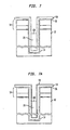
- a fill material 60 is deposited to form storage node 20 by filling trench 14.
- a second barrier layer 59 of Silicon Nitride may be deposited in order to prevent oxidation of the fill materials.
- Fill material 60 is preferably polysilicon.
- Layer 58 and barrier layer 56 are removed in areas not protected by fill material 60 by a wet etching process, for example an HF etch as shown in FIG. 8 .
- the fill material is recessed to form collar 42 as described herein above ( FIG. 2 ).
- remaining in trench 14 is barrier layer 56 and layer 58 forming a dielectric in accordance with the present invention. Further processing continues as is known in the art.
- ⁇ for rutile is between about 86 to about 170 (polycrystalline rutile has a dielectric constant of about 110), and the amount of leakage current (which depends on the crystallographic orientation and quality of the rutile film) is reduced.
Landscapes
- Engineering & Computer Science (AREA)
- Manufacturing & Machinery (AREA)
- Semiconductor Memories (AREA)
- Semiconductor Integrated Circuits (AREA)
- Crystals, And After-Treatments Of Crystals (AREA)
Claims (15)
- Verfahren zur Bildung von Halbleiterbauelementen, mit den folgenden Schritten:Bereitstellen eines tiefen Grabens (14) in einem Substrat (12), wobei der tiefe Graben einen unteren Teil aufweist;Ausheilen des Substrats (12), um native Oxide von der Oberfläche des tiefen Grabens zu entfernen;Bilden einer ersten Barrierenschicht (56) in dem tiefen Graben durch Auskleiden des tiefen Grabens nach dem Ausheilen des Substrats, wobei die erste Barrierenschicht eine Siliziumnitridschicht ist und eine Dicke von weniger als etwa 1 nm aufweist;Bilden einer dielektrischen Schicht (58) auf der ersten Barrierenschicht in dem tiefen Graben durch Auskleiden des tiefen Grabens, wobei die dielektrische Schicht Titandioxid in der Rutil-Kristallform umfasst;Füllen eines Teils des tiefen Grabens mit einem leitfähigen Füllmaterial (60), um dadurch einen Speicherknoten zu bilden; undEntfernen eines Teils der ersten Barrierenschicht und der dielektrischen Schicht dergestalt, dass die dielektrische Schicht (58) und die Barrierenschicht (56) den unteren Teil des tiefen Grabens (14) auskleiden.
- Verfahren nach Anspruch 1, wobei der Schritt des Ausheilens des Substrats (12) in einer Wasserstoff-Umgebung ausgeführt wird.
- Verfahren nach Anspruch 2, wobei die Temperatur des Ausheilens zwischen 600°C und 800°C liegt.
- Verfahren nach Anspruch 1, wobei der Schritt des Bildens der ersten Barrierenschicht (56) den Schritt umfasst, den Graben (14) bei einer Temperatur im Bereich von mindestens etwa 500°C bis zu höchstens etwa 700°C einer NH3-Umgebung auszusetzen.
- Verfahren nach Anspruch 4, wobei der Schritt des Ausheilens und der Schritt des Bildens der ersten Barrierenschicht (56) in einem gemeinsamen Behälter ausgeführt werden.
- Verfahren nach Anspruch 1, wobei der Schritt des Bildens der dielektrischen Schicht (58) den Schritt umfasst, eine Titandioxidschicht durch chemische Aufdampfung abzuscheiden.
- Verfahren nach Anspruch 6, ferner mit den folgenden Schritten:Oxidieren der Titandioxidschicht (58); undAusheilen der Titandioxidschicht (58), wobei die ordnungsgemäße 1:2-Stoichiometrie und Rutil-Kristallstruktur erzielt werden.
- Verfahren nach Anspruch 7, ferner mit dem Schritt des Bereitstellens eines Vorläufermaterials vor der Bildung von Rutil (Ti02), umfassend TDMAT (Tetrakis(dimethylamido)titan), TDEAT (Tetrakis(diethylamido)titan), Ti(O-iPr)4(tdh)2(bis(isopropoxy)bis(tetramethylheptandionato)titan oder Titantetrachlorid.
- Verfahren nach Anspruch 1, wobei der Schritt des Bildens des Titandioxids Folgendes umfasst:Abscheiden einer Schicht aus TiN in dem unteren Teil des tiefen Grabens; undOxidieren der Schicht aus TiN, um Titandioxid in der Rutilform zu bilden.
- Verfahren nach Anspruch 9, wobei der Schritt des Oxidierens den Schritt des Oxidierens der Schicht aus TiN durch Plasmaoxidation umfasst.
- Verfahren nach Anspruch 9, wobei der Schritt des Oxidierens den Schritt des Oxidierens der Schicht aus TiN durch schnelle thermische Oxidation umfasst.
- Verfahren nach Anspruch 1, ferner mit dem folgenden Schritt:Abscheiden einer zweiten Barrierenschicht (59) über der dielektrischen Schicht (58) vor dem Schritt des teilweisen Füllens des tiefen Grabens mit einem leitfähigen Füllmaterial (60), um dadurch einen Speicherknoten zu bilden.
- Verfahren nach Anspruch 7, wobei der Ausheilschritt bei einer Temperatur im Bereich von etwa 750°C bis etwa 1050°C ausgeführt wird.
- Halbleiterbauelement, umfassend:ein Substrat (12) mit einem darin gebildeten Graben (14);ein leitfähiges Füllmaterial (60), das einen Teil des Grabens (14) füllt und kapazitiv mit dem Substrat (12) gekoppelt ist, wobei das leitfähige Füllmaterial einen Speicherknoten bildet; eine Barrierenschicht (56) in dem Graben (14) zwischen dem leitfähigen Füllmaterial (60) und dem Substrat (12), wobei die Barrierenschicht (56) einen unteren Teil des Grabens (14) auskleidet; wobei die Barrierenschicht (56) eine Siliziumnitridschicht ist und eine Dicke von weniger als etwa 1 nm aufweist; undeine dielektrische Schicht (58) in dem Graben (14) zwischen dem leitfähigen Füllmaterial und der Barrierenschicht (56), die den unteren Teil des Grabens (14) auskleidet, wobei die dielektrische Schicht (56) Titanoxid in der Rutil-Kristallform umfasst.
- Halbleiterbauelement nach Anspruch 14, wobei das Titanoxid (58) eine Dicke von zwischen etwa 15 Nanometer bis etwa 35 Nanometer aufweist.
Applications Claiming Priority (2)
| Application Number | Priority Date | Filing Date | Title |
|---|---|---|---|
| US193203 | 1998-11-17 | ||
| US09/193,203 US6156606A (en) | 1998-11-17 | 1998-11-17 | Method of forming a trench capacitor using a rutile dielectric material |
Publications (3)
| Publication Number | Publication Date |
|---|---|
| EP1003206A2 EP1003206A2 (de) | 2000-05-24 |
| EP1003206A3 EP1003206A3 (de) | 2000-09-20 |
| EP1003206B1 true EP1003206B1 (de) | 2010-05-12 |
Family
ID=22712639
Family Applications (1)
| Application Number | Title | Priority Date | Filing Date |
|---|---|---|---|
| EP99119456A Expired - Lifetime EP1003206B1 (de) | 1998-11-17 | 1999-09-30 | Rutil-Dielektrikum für Halbleiter-Bauelement |
Country Status (7)
| Country | Link |
|---|---|
| US (1) | US6156606A (de) |
| EP (1) | EP1003206B1 (de) |
| JP (1) | JP2000150817A (de) |
| KR (1) | KR100665429B1 (de) |
| CN (1) | CN1149647C (de) |
| DE (1) | DE69942361D1 (de) |
| TW (1) | TW440916B (de) |
Families Citing this family (68)
| Publication number | Priority date | Publication date | Assignee | Title |
|---|---|---|---|---|
| JP3246887B2 (ja) * | 1997-09-05 | 2002-01-15 | 日本製紙株式会社 | インクジェット記録のためのキャストコート紙用基材、及びそれを用いたキャストコート紙 |
| DE59802105D1 (de) * | 1998-06-18 | 2001-12-06 | Ilford Imaging Ch Gmbh | Aufzeichnungsmaterialien für den Tintenstrahldruck |
| US6825087B1 (en) * | 1999-11-24 | 2004-11-30 | Fairchild Semiconductor Corporation | Hydrogen anneal for creating an enhanced trench for trench MOSFETS |
| US6461918B1 (en) | 1999-12-20 | 2002-10-08 | Fairchild Semiconductor Corporation | Power MOS device with improved gate charge performance |
| EP1150350A3 (de) * | 2000-02-25 | 2002-04-24 | Infineon Technologies North America Corp. | Herstellung eines Grabenkondensators |
| US6348373B1 (en) * | 2000-03-29 | 2002-02-19 | Sharp Laboratories Of America, Inc. | Method for improving electrical properties of high dielectric constant films |
| US7745289B2 (en) | 2000-08-16 | 2010-06-29 | Fairchild Semiconductor Corporation | Method of forming a FET having ultra-low on-resistance and low gate charge |
| US6368970B1 (en) * | 2000-08-24 | 2002-04-09 | Infineon Technologies Ag | Semiconductor configuration and corresponding production process |
| US6420230B1 (en) | 2000-08-31 | 2002-07-16 | Micron Technology, Inc. | Capacitor fabrication methods and capacitor constructions |
| US7112503B1 (en) * | 2000-08-31 | 2006-09-26 | Micron Technology, Inc. | Enhanced surface area capacitor fabrication methods |
| US7217615B1 (en) * | 2000-08-31 | 2007-05-15 | Micron Technology, Inc. | Capacitor fabrication methods including forming a conductive layer |
| US6710403B2 (en) | 2002-07-30 | 2004-03-23 | Fairchild Semiconductor Corporation | Dual trench power MOSFET |
| US7345342B2 (en) | 2001-01-30 | 2008-03-18 | Fairchild Semiconductor Corporation | Power semiconductor devices and methods of manufacture |
| US7132712B2 (en) | 2002-11-05 | 2006-11-07 | Fairchild Semiconductor Corporation | Trench structure having one or more diodes embedded therein adjacent a PN junction |
| US6818513B2 (en) | 2001-01-30 | 2004-11-16 | Fairchild Semiconductor Corporation | Method of forming a field effect transistor having a lateral depletion structure |
| US6677641B2 (en) | 2001-10-17 | 2004-01-13 | Fairchild Semiconductor Corporation | Semiconductor structure with improved smaller forward voltage loss and higher blocking capability |
| US6916745B2 (en) | 2003-05-20 | 2005-07-12 | Fairchild Semiconductor Corporation | Structure and method for forming a trench MOSFET having self-aligned features |
| US6803626B2 (en) | 2002-07-18 | 2004-10-12 | Fairchild Semiconductor Corporation | Vertical charge control semiconductor device |
| DE10114956C2 (de) | 2001-03-27 | 2003-06-18 | Infineon Technologies Ag | Verfahren zum Herstellen einer dielektrischen Schicht als Isolatorschicht für einen Grabenkondensator |
| TW564550B (en) * | 2001-06-05 | 2003-12-01 | Hitachi Ltd | Semiconductor device |
| DE10130936B4 (de) * | 2001-06-27 | 2004-04-29 | Infineon Technologies Ag | Herstellungsverfahren für ein Halbleiterbauelement mittels Atomschichtabscheidung/ALD |
| US6432725B1 (en) | 2001-09-28 | 2002-08-13 | Infineon Technologies Ag | Methods for crystallizing metallic oxide dielectric films at low temperature |
| TW501206B (en) * | 2001-10-03 | 2002-09-01 | Promos Technologies Inc | Manufacturing method of buried strap diffusion area |
| US7061066B2 (en) | 2001-10-17 | 2006-06-13 | Fairchild Semiconductor Corporation | Schottky diode using charge balance structure |
| US6750156B2 (en) | 2001-10-24 | 2004-06-15 | Applied Materials, Inc. | Method and apparatus for forming an anti-reflective coating on a substrate |
| US7078296B2 (en) | 2002-01-16 | 2006-07-18 | Fairchild Semiconductor Corporation | Self-aligned trench MOSFETs and methods for making the same |
| DE10202140A1 (de) * | 2002-01-21 | 2003-08-07 | Infineon Technologies Ag | Verfahren zum Herstellen eines Hohlraums in einem monokristallinen Siliziumsubstrat und Halbleiterbaustein mit einem Hohlraum in einem monokristallinen Siliziumsubstrat mit einer epitaktischen Deckschicht |
| KR100859701B1 (ko) | 2002-02-23 | 2008-09-23 | 페어차일드코리아반도체 주식회사 | 고전압 수평형 디모스 트랜지스터 및 그 제조 방법 |
| AU2003270452A1 (en) * | 2002-09-02 | 2004-03-19 | Advanced Micro Devices, Inc. | Transistor element having an anisotropic high-k gate dielectric |
| US7033891B2 (en) | 2002-10-03 | 2006-04-25 | Fairchild Semiconductor Corporation | Trench gate laterally diffused MOSFET devices and methods for making such devices |
| US7576388B1 (en) | 2002-10-03 | 2009-08-18 | Fairchild Semiconductor Corporation | Trench-gate LDMOS structures |
| US6710418B1 (en) | 2002-10-11 | 2004-03-23 | Fairchild Semiconductor Corporation | Schottky rectifier with insulation-filled trenches and method of forming the same |
| US7638841B2 (en) | 2003-05-20 | 2009-12-29 | Fairchild Semiconductor Corporation | Power semiconductor devices and methods of manufacture |
| US7440255B2 (en) | 2003-07-21 | 2008-10-21 | Micron Technology, Inc. | Capacitor constructions and methods of forming |
| KR100994719B1 (ko) | 2003-11-28 | 2010-11-16 | 페어차일드코리아반도체 주식회사 | 슈퍼정션 반도체장치 |
| US7087517B2 (en) * | 2003-12-24 | 2006-08-08 | Intel Corporation | Method to fabricate interconnect structures |
| US7368777B2 (en) | 2003-12-30 | 2008-05-06 | Fairchild Semiconductor Corporation | Accumulation device with charge balance structure and method of forming the same |
| US7410864B2 (en) * | 2004-04-23 | 2008-08-12 | Infineon Technologies Ag | Trench and a trench capacitor and method for forming the same |
| US7352036B2 (en) | 2004-08-03 | 2008-04-01 | Fairchild Semiconductor Corporation | Semiconductor power device having a top-side drain using a sinker trench |
| US7172947B2 (en) * | 2004-08-31 | 2007-02-06 | Micron Technology, Inc | High dielectric constant transition metal oxide materials |
| US7265415B2 (en) | 2004-10-08 | 2007-09-04 | Fairchild Semiconductor Corporation | MOS-gated transistor with reduced miller capacitance |
| DE112006000832B4 (de) | 2005-04-06 | 2018-09-27 | Fairchild Semiconductor Corporation | Trenched-Gate-Feldeffekttransistoren und Verfahren zum Bilden derselben |
| DE112006001516T5 (de) | 2005-06-10 | 2008-04-17 | Fairchild Semiconductor Corp. | Feldeffekttransistor mit Ladungsgleichgewicht |
| US7385248B2 (en) | 2005-08-09 | 2008-06-10 | Fairchild Semiconductor Corporation | Shielded gate field effect transistor with improved inter-poly dielectric |
| ITTO20050630A1 (it) * | 2005-09-15 | 2007-03-16 | St Microelectronics Srl | Dispositivo di potenza a semiconduttore a porta isolata formata in uno scavo e relativo procedimento di fabbricazione |
| US7446374B2 (en) | 2006-03-24 | 2008-11-04 | Fairchild Semiconductor Corporation | High density trench FET with integrated Schottky diode and method of manufacture |
| US7416952B2 (en) * | 2006-05-23 | 2008-08-26 | Infineon Technologies Ag | Method for producing a dielectric interlayer and storage capacitor with such a dielectric interlayer |
| US7319256B1 (en) | 2006-06-19 | 2008-01-15 | Fairchild Semiconductor Corporation | Shielded gate trench FET with the shield and gate electrodes being connected together |
| JP2010541212A (ja) | 2007-09-21 | 2010-12-24 | フェアチャイルド・セミコンダクター・コーポレーション | 電力デバイスのための超接合構造及び製造方法 |
| US7772668B2 (en) | 2007-12-26 | 2010-08-10 | Fairchild Semiconductor Corporation | Shielded gate trench FET with multiple channels |
| US20120273916A1 (en) | 2011-04-27 | 2012-11-01 | Yedinak Joseph A | Superjunction Structures for Power Devices and Methods of Manufacture |
| US8174067B2 (en) | 2008-12-08 | 2012-05-08 | Fairchild Semiconductor Corporation | Trench-based power semiconductor devices with increased breakdown voltage characteristics |
| US7851312B2 (en) * | 2009-01-23 | 2010-12-14 | Semiconductor Components Industries, Llc | Semiconductor component and method of manufacture |
| JP2011034995A (ja) * | 2009-07-29 | 2011-02-17 | Elpida Memory Inc | 半導体装置の製造方法及び半導体装置 |
| JP4988902B2 (ja) | 2009-07-31 | 2012-08-01 | 株式会社日立国際電気 | 半導体デバイスの製造方法及び基板処理装置 |
| JP5460775B2 (ja) * | 2009-07-31 | 2014-04-02 | 株式会社日立国際電気 | 半導体デバイスの製造方法、半導体デバイス及び基板処理装置 |
| US8518486B2 (en) | 2010-05-12 | 2013-08-27 | Micron Technology, Inc. | Methods of forming and utilizing rutile-type titanium oxide |
| US8432000B2 (en) | 2010-06-18 | 2013-04-30 | Fairchild Semiconductor Corporation | Trench MOS barrier schottky rectifier with a planar surface using CMP techniques |
| KR20120051820A (ko) * | 2010-11-15 | 2012-05-23 | 삼성전자주식회사 | 커패시터, 그 형성 방법, 이를 포함하는 반도체 소자 및 그 제조 방법 |
| US8564095B2 (en) | 2011-02-07 | 2013-10-22 | Micron Technology, Inc. | Capacitors including a rutile titanium dioxide material and semiconductor devices incorporating same |
| US8609553B2 (en) | 2011-02-07 | 2013-12-17 | Micron Technology, Inc. | Methods of forming rutile titanium dioxide and associated methods of forming semiconductor structures |
| US8836028B2 (en) | 2011-04-27 | 2014-09-16 | Fairchild Semiconductor Corporation | Superjunction structures for power devices and methods of manufacture |
| US8673700B2 (en) | 2011-04-27 | 2014-03-18 | Fairchild Semiconductor Corporation | Superjunction structures for power devices and methods of manufacture |
| US8772868B2 (en) | 2011-04-27 | 2014-07-08 | Fairchild Semiconductor Corporation | Superjunction structures for power devices and methods of manufacture |
| US8786010B2 (en) | 2011-04-27 | 2014-07-22 | Fairchild Semiconductor Corporation | Superjunction structures for power devices and methods of manufacture |
| US8828836B2 (en) * | 2011-06-06 | 2014-09-09 | Intermolecular, Inc. | Method for fabricating a DRAM capacitor |
| US9178011B2 (en) | 2013-03-13 | 2015-11-03 | Intermolecular, Inc. | Deposition of anisotropic dielectric layers orientationally matched to the physically separated substrate |
| KR102406971B1 (ko) * | 2015-12-24 | 2022-06-10 | 삼성전자주식회사 | 커패시터를 포함하는 반도체 장치 및 이의 제조 방법 |
Family Cites Families (11)
| Publication number | Priority date | Publication date | Assignee | Title |
|---|---|---|---|---|
| US4200474A (en) * | 1978-11-20 | 1980-04-29 | Texas Instruments Incorporated | Method of depositing titanium dioxide (rutile) as a gate dielectric for MIS device fabrication |
| JPS6338248A (ja) * | 1986-08-04 | 1988-02-18 | Hitachi Ltd | 半導体装置およびその製造方法 |
| US4870539A (en) * | 1989-01-17 | 1989-09-26 | International Business Machines Corporation | Doped titanate glass-ceramic for grain boundary barrier layer capacitors |
| US5143861A (en) * | 1989-03-06 | 1992-09-01 | Sgs-Thomson Microelectronics, Inc. | Method making a dynamic random access memory cell with a tungsten plug |
| US5202152A (en) * | 1991-10-25 | 1993-04-13 | Cornell Research Foundation, Inc. | Synthesis of titanium nitride films |
| US5376223A (en) * | 1992-01-09 | 1994-12-27 | Varian Associates, Inc. | Plasma etch process |
| JP2897631B2 (ja) * | 1993-12-28 | 1999-05-31 | 日本電気株式会社 | 半導体集積回路装置および製造方法 |
| JPH07263572A (ja) * | 1994-03-23 | 1995-10-13 | Hitachi Ltd | 半導体メモリ装置の製造方法及び半導体メモリ装置並びにそれを用いた応用システム |
| JP3146962B2 (ja) * | 1995-12-14 | 2001-03-19 | 日本電気株式会社 | 半導体記憶装置およびその製造方法 |
| US5793075A (en) * | 1996-07-30 | 1998-08-11 | International Business Machines Corporation | Deep trench cell capacitor with inverting counter electrode |
| EP0843361A1 (de) * | 1996-11-15 | 1998-05-20 | Hitachi Europe Limited | Speicheranordnung |
-
1998
- 1998-11-17 US US09/193,203 patent/US6156606A/en not_active Expired - Fee Related
-
1999
- 1999-09-30 EP EP99119456A patent/EP1003206B1/de not_active Expired - Lifetime
- 1999-09-30 DE DE69942361T patent/DE69942361D1/de not_active Expired - Lifetime
- 1999-11-15 TW TW088119875A patent/TW440916B/zh not_active IP Right Cessation
- 1999-11-16 KR KR1019990050784A patent/KR100665429B1/ko not_active Expired - Fee Related
- 1999-11-17 CN CNB991248279A patent/CN1149647C/zh not_active Expired - Fee Related
- 1999-11-17 JP JP11327135A patent/JP2000150817A/ja not_active Withdrawn
Also Published As
| Publication number | Publication date |
|---|---|
| US6156606A (en) | 2000-12-05 |
| KR100665429B1 (ko) | 2007-01-04 |
| EP1003206A2 (de) | 2000-05-24 |
| CN1149647C (zh) | 2004-05-12 |
| TW440916B (en) | 2001-06-16 |
| DE69942361D1 (de) | 2010-06-24 |
| CN1270414A (zh) | 2000-10-18 |
| KR20000035492A (ko) | 2000-06-26 |
| EP1003206A3 (de) | 2000-09-20 |
| JP2000150817A (ja) | 2000-05-30 |
Similar Documents
| Publication | Publication Date | Title |
|---|---|---|
| EP1003206B1 (de) | Rutil-Dielektrikum für Halbleiter-Bauelement | |
| US6300215B1 (en) | Methods of forming integrated circuit capacitors having composite titanium oxide and tantalum pentoxide dielectric layers therein | |
| US6352892B2 (en) | Method of making DRAM trench capacitor | |
| US6437381B1 (en) | Semiconductor memory device with reduced orientation-dependent oxidation in trench structures | |
| US7872294B2 (en) | Semiconductor device having a capacitance element and method of manufacturing the same | |
| US6555430B1 (en) | Process flow for capacitance enhancement in a DRAM trench | |
| US6303432B1 (en) | Method of manufacturing a semiconductor device | |
| US5897352A (en) | Method of manufacturing hemispherical grained polysilicon with improved adhesion and reduced capacitance depletion | |
| US6057189A (en) | Method of fabricating capacitor utilizing an ion implantation method | |
| US6458647B1 (en) | Process flow for sacrificial collar with poly mask | |
| US7223669B2 (en) | Structure and method for collar self-aligned to buried plate | |
| US6770526B2 (en) | Silicon nitride island formation for increased capacitance | |
| US6620675B2 (en) | Increased capacitance trench capacitor | |
| US6930345B2 (en) | Increase in deep trench capacitance by a central ground electrode | |
| US5466627A (en) | Stacked capacitor process using BPSG precipitates | |
| JP2000196035A (ja) | メモリ素子のキャパシタ製造方法 | |
| US6251725B1 (en) | Method of fabricating a DRAM storage node on a semiconductor wafer | |
| HK1024783A (en) | Rutile dielectric material for semiconductor devices | |
| US20050062111A1 (en) | Maskless middle-of-line liner deposition | |
| US20050017282A1 (en) | Dram buried strap process with silicon carbide | |
| KR100247227B1 (ko) | 전극들간의 인가전압에 관해 안정된 캐패시턴스를 가지는 굴곡형 다결정 실리콘 전극상의 고유전체 스토리지 캐패시터 및 그 제조방법 | |
| KR100249917B1 (ko) | Dram셀의 커패시터의 제조방법 | |
| US20040126964A1 (en) | Method for fabricating capacitor in semiconductor device | |
| JPH10275900A (ja) | 半導体装置の製造方法 | |
| KR20030094428A (ko) | 반도체 소자의 커패시터 형성방법 |
Legal Events
| Date | Code | Title | Description |
|---|---|---|---|
| PUAI | Public reference made under article 153(3) epc to a published international application that has entered the european phase |
Free format text: ORIGINAL CODE: 0009012 |
|
| AK | Designated contracting states |
Kind code of ref document: A2 Designated state(s): AT BE CH CY DE DK ES FI FR GB GR IE IT LI LU MC NL PT SE |
|
| AX | Request for extension of the european patent |
Free format text: AL;LT;LV;MK;RO;SI |
|
| RIN1 | Information on inventor provided before grant (corrected) |
Inventor name: MICHAELIS, ALEXANDER |
|
| PUAL | Search report despatched |
Free format text: ORIGINAL CODE: 0009013 |
|
| AK | Designated contracting states |
Kind code of ref document: A3 Designated state(s): AT BE CH CY DE DK ES FI FR GB GR IE IT LI LU MC NL PT SE |
|
| AX | Request for extension of the european patent |
Free format text: AL;LT;LV;MK;RO;SI |
|
| 17P | Request for examination filed |
Effective date: 20010313 |
|
| AKX | Designation fees paid |
Free format text: DE FR GB IE IT NL |
|
| RAP1 | Party data changed (applicant data changed or rights of an application transferred) |
Owner name: INFINEON TECHNOLOGIES AG |
|
| 17Q | First examination report despatched |
Effective date: 20060118 |
|
| REG | Reference to a national code |
Ref country code: HK Ref legal event code: WD Ref document number: 1024783 Country of ref document: HK |
|
| 17Q | First examination report despatched |
Effective date: 20060118 |
|
| GRAP | Despatch of communication of intention to grant a patent |
Free format text: ORIGINAL CODE: EPIDOSNIGR1 |
|
| GRAS | Grant fee paid |
Free format text: ORIGINAL CODE: EPIDOSNIGR3 |
|
| GRAA | (expected) grant |
Free format text: ORIGINAL CODE: 0009210 |
|
| AK | Designated contracting states |
Kind code of ref document: B1 Designated state(s): DE FR GB IE IT NL |
|
| REG | Reference to a national code |
Ref country code: GB Ref legal event code: FG4D |
|
| RAP2 | Party data changed (patent owner data changed or rights of a patent transferred) |
Owner name: INFINEON TECHNOLOGIES AG |
|
| REG | Reference to a national code |
Ref country code: IE Ref legal event code: FG4D |
|
| REF | Corresponds to: |
Ref document number: 69942361 Country of ref document: DE Date of ref document: 20100624 Kind code of ref document: P |
|
| REG | Reference to a national code |
Ref country code: NL Ref legal event code: VDEP Effective date: 20100512 |
|
| PG25 | Lapsed in a contracting state [announced via postgrant information from national office to epo] |
Ref country code: NL Free format text: LAPSE BECAUSE OF FAILURE TO SUBMIT A TRANSLATION OF THE DESCRIPTION OR TO PAY THE FEE WITHIN THE PRESCRIBED TIME-LIMIT Effective date: 20100512 |
|
| PGFP | Annual fee paid to national office [announced via postgrant information from national office to epo] |
Ref country code: DE Payment date: 20101018 Year of fee payment: 12 |
|
| PLBE | No opposition filed within time limit |
Free format text: ORIGINAL CODE: 0009261 |
|
| STAA | Information on the status of an ep patent application or granted ep patent |
Free format text: STATUS: NO OPPOSITION FILED WITHIN TIME LIMIT |
|
| PG25 | Lapsed in a contracting state [announced via postgrant information from national office to epo] |
Ref country code: IT Free format text: LAPSE BECAUSE OF FAILURE TO SUBMIT A TRANSLATION OF THE DESCRIPTION OR TO PAY THE FEE WITHIN THE PRESCRIBED TIME-LIMIT Effective date: 20100512 |
|
| 26N | No opposition filed |
Effective date: 20110215 |
|
| GBPC | Gb: european patent ceased through non-payment of renewal fee |
Effective date: 20100930 |
|
| REG | Reference to a national code |
Ref country code: DE Ref legal event code: R097 Ref document number: 69942361 Country of ref document: DE Effective date: 20110214 |
|
| REG | Reference to a national code |
Ref country code: FR Ref legal event code: ST Effective date: 20110531 |
|
| PG25 | Lapsed in a contracting state [announced via postgrant information from national office to epo] |
Ref country code: IE Free format text: LAPSE BECAUSE OF NON-PAYMENT OF DUE FEES Effective date: 20100930 Ref country code: FR Free format text: LAPSE BECAUSE OF NON-PAYMENT OF DUE FEES Effective date: 20100930 |
|
| PG25 | Lapsed in a contracting state [announced via postgrant information from national office to epo] |
Ref country code: GB Free format text: LAPSE BECAUSE OF NON-PAYMENT OF DUE FEES Effective date: 20100930 |
|
| REG | Reference to a national code |
Ref country code: DE Ref legal event code: R081 Ref document number: 69942361 Country of ref document: DE Owner name: QIMONDA AG, DE Free format text: FORMER OWNER: INFINEON TECHNOLOGIES AG, 85579 NEUBIBERG, DE Effective date: 20111208 |
|
| REG | Reference to a national code |
Ref country code: DE Ref legal event code: R119 Ref document number: 69942361 Country of ref document: DE Effective date: 20120403 |
|
| PG25 | Lapsed in a contracting state [announced via postgrant information from national office to epo] |
Ref country code: DE Free format text: LAPSE BECAUSE OF NON-PAYMENT OF DUE FEES Effective date: 20120403 |