EP1014353A2 - Initialisierung eines optischen Aufziechnungsmediums von Phasenwechseltyp - Google Patents
Initialisierung eines optischen Aufziechnungsmediums von Phasenwechseltyp Download PDFInfo
- Publication number
- EP1014353A2 EP1014353A2 EP99125824A EP99125824A EP1014353A2 EP 1014353 A2 EP1014353 A2 EP 1014353A2 EP 99125824 A EP99125824 A EP 99125824A EP 99125824 A EP99125824 A EP 99125824A EP 1014353 A2 EP1014353 A2 EP 1014353A2
- Authority
- EP
- European Patent Office
- Prior art keywords
- recording medium
- width
- laser device
- half maximum
- distribution
- Prior art date
- Legal status (The legal status is an assumption and is not a legal conclusion. Google has not performed a legal analysis and makes no representation as to the accuracy of the status listed.)
- Granted
Links
Images


Classifications
-
- G—PHYSICS
- G11—INFORMATION STORAGE
- G11B—INFORMATION STORAGE BASED ON RELATIVE MOVEMENT BETWEEN RECORD CARRIER AND TRANSDUCER
- G11B7/00—Recording or reproducing by optical means, e.g. recording using a thermal beam of optical radiation by modifying optical properties or the physical structure, reproducing using an optical beam at lower power by sensing optical properties; Record carriers therefor
- G11B7/24—Record carriers characterised by shape, structure or physical properties, or by the selection of the material
- G11B7/26—Apparatus or processes specially adapted for the manufacture of record carriers
- G11B7/268—Post-production operations, e.g. initialising phase-change recording layers, checking for defects
-
- G—PHYSICS
- G11—INFORMATION STORAGE
- G11B—INFORMATION STORAGE BASED ON RELATIVE MOVEMENT BETWEEN RECORD CARRIER AND TRANSDUCER
- G11B7/00—Recording or reproducing by optical means, e.g. recording using a thermal beam of optical radiation by modifying optical properties or the physical structure, reproducing using an optical beam at lower power by sensing optical properties; Record carriers therefor
- G11B7/12—Heads, e.g. forming of the optical beam spot or modulation of the optical beam
- G11B7/125—Optical beam sources therefor, e.g. laser control circuitry specially adapted for optical storage devices; Modulators, e.g. means for controlling the size or intensity of optical spots or optical traces
- G11B7/127—Lasers; Multiple laser arrays
Definitions
- the present invention relates to a method of initializing an information recording medium by irradiating light beams, and particularly to, the method for a rewritable phase-change optical recording layer that is capable of giving rise to a phase change to achieve repeated read-write operations by laser beam irradiation.
- Optical recording media have recently come into wide use as a viable information storage and archival means of large capacity.
- demands have increased on a phase-change optical recording medium for use in a CD-R disk, for example, because of its repeatable (or writable) read/write capability.
- the phase-change optical recording medium is generally provided on a disk-shaped substrate with several layers successively formed by, for example, the sputtering method, such as a first dielectric layer, a recording layer, a second dielectric layer and a layer either of metal or alloy, in the order recited.
- a layer composed of ultraviolet curing resin is formed thereon by spin coating, for example.
- process steps of crystallization are to be carried out before recording onto the recording layer by a recording system or disk drive.
- the recording layer is once heated to a temperature above its melting temperature.
- the recording layer is then cooled relatively slowly, it transforms into a crystalline state, while it transforms into an amorphous state, when cooled rapidly.
- carbonate resin is frequently used for its excellent properties such as mechanical stability, light in weight and low costs, among others.
- the initialization steps are generally carried out gradually over the disk area, in which disk portions are successively irradiated by a focused intense beam from a laser device along with the rotation of the disk.
- the initialization of an optical disk is achieved by providing a laser device with its longer axis of the power distribution perpendicular to disk tracks and by imparting a gradual displacement of the laser device along the radial direction of the disk (i.e., perpendicular to the direction of disk tracks).
- reflectivity values of the optical disk after the initialization may undesirably fluctuate along the perpendicular direction. This may result in scatter in tracking signals, which is a drawback throughout successive reading and signal processing steps of the optical disk.
- the present inventors first examined closely initialization process steps of a phase-change optical disk as follows.
- an improved method of initializing a phase-change optical information recording medium is provided, using an optical system incorporating a semiconductor laser device.
- the laser device disclosed herein is characterized by its specified spatial power distribution. Namely, in the spatial distribution of laser power focused on the recording medium in the direction perpendicular to guide tracks, the laser device preferably has an average smaller in both end regions of the distribution, each of which corresponds to 10% of the width at half maximum of the distribution, than the average in the center region of the full width at half maximum of the distribution.
- edge surfaces substantially perpendicular to the direction of the laser emission, of at least one of an active layer and a reflective layer of the semiconductor laser device may preferably be polished such that an appropriate spatial laser power distribution such as mentioned above can be obtained.
- the optical system used in the disk initialization is further provided at least one optical unit such as, for example, a filter which is capable of attenuating the laser beam intensity so as to achieve an appropriate laser power distribution.
- at least one optical unit such as, for example, a filter which is capable of attenuating the laser beam intensity so as to achieve an appropriate laser power distribution.
- the laser device may be cured for at least about six hours by being energized with at least about 80% of a maximum allowable electric power prior to the initialization of the recording medium so as to attain an appropriate laser power distribution.
- the displacement step of the an initialization head unit including the laser device is preferably larger than one half of, and smaller than, the width at half maximum of the spatial laser power distribution.
- the laser device preferably has emitted light beams having the width at half maximum of at least 80 microns in the spatial power distribution focused on the recording medium in the direction perpendicular to guide tracks.
- a homogeneous crystallization and concomitant reflectivity of the recording layer can be achieved in the optical disk through initialization steps.
- excellent characteristics of tracking signals and outputted data signals after the disk initialization can be achieved with thus initialized optical disks in a reduced initialization time, thereby increasing productivity of the optical disk.
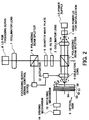
- FIG. 1 is a cross-sectional view illustrating a basic configuration of a phase-change optical disk.
- a phase-change optical disk includes a substrate 51 having a pregrooved guide track, with the following layers formed thereon in the order recited, a first dielectric layer 52, a recording layer 53, a second dielectric layer 54, a reflective/heat-dissipating layer 55, and an overcoat layer 56.
- the optical disk may further include a printed layer 57 formed on the overcoat layer 56 and a hard coat layer 58 formed on the backside of the substrate 1.
- Suitable materials for use as the substrate 1 include glass, ceramics, resins and similar materials. Among these, resins may preferably be employed for its satisfactory features, such as easy for molding, low in costs and light in weight. Specific examples of the resins include, but are not limited to, polycarbonate resins and acrylic resins.
- the substrate 1 is formed in disc-shaped, in general, and may also be either in card- or sheet-shaped.
- the substrate 1 preferably has a thickness of 1.2 mm or 0.6 mm, but not limited thereto.
- first dielectric layer 52, recording layer 53 and second dielectric layer 54 are formed by, for example, the sputtering method, while the overcoat layer 56 is formed by coating an ultraviolet curing resin composition.
- Suitable materials for use in the recording layer 53 is preferably a quaternary compound containing Ag, In, Sb and Te, as the main ingredient, which is capable of forming a phase-change recording composition.
- This material can adequately be used in the recording layer for its excellent characteristics such as high sensitivity and speed of either recording or erasing and erasure ratio.
- recording is achieved for the recording layer to be brought into an amorphous state, while erasing is achieved likewise into a crystalline state.
- the recording layer 53 preferably has a thickness of 15 to 35 nanometers.
- Suitable materials for use in the first dielectric layer 52 and second dielectric layer 54 include SiO, SiO 2 , TiO 2 and other oxides; Si 3 N 4 , AlN and other nitrides; ZnS, In 2 S 3 and other sulfides; SiC, TaC and other carbides; and diamond-like carbon.
- the first dielectric layer preferably has a thickness of 65 to 130 nanometers, while the second dielectric layers has a thickness of 15 to 45 nanometers,
- the reflective/heat-dissipating layer 55 materials preferably used are Al, Au, Ag, Cu, Ta and other metals, and alloys formed in combination thereof.
- This layer preferably has a thickness of 7 to 180 nanometers.
- an ultraviolet curing resin material is spin coated, in general, to have a thickness of 7 to 15 nanometers.
- laser light As electromagnetic radiation and energy beams useful for initialization of the information data recording medium discussed herein, laser light, electron beams, ultraviolet light, visible light, infrared light and microwave radiation may be utilized.
- light beams from a semiconductor laser device i.e., laser diode or LD
- LD laser diode
- the apparatus for the initialization includes a rotating mechanism for rotating a optical disk, a driving mechanism for radially displacing the rotation axis of the optical disk, a light emitting (LD) unit, a focussing mechanism for focussing laser beams onto a recording layer on the optical disk, a control system for electrically controlling the entire apparatus.
- a rotating mechanism for rotating a optical disk a driving mechanism for radially displacing the rotation axis of the optical disk
- a light emitting (LD) unit for radially displacing the rotation axis of the optical disk
- LD light emitting
- focussing mechanism for focussing laser beams onto a recording layer on the optical disk
- control system for electrically controlling the entire apparatus.
- a recording layer in an optical disk is formed as an amorphous state after the layer forming step by, for example, sputtering method.
- the recording layer in the amorphous state is transformed into a crystalline state by laser beam heating and following quenching steps. Further, the optical disk can be initialized efficiently by simultaneously heating the recording layer portions located on a plurality of, for example, more than ten, pregrooved guide tracks of the rotating optical disk.
- the initialization is preferably carried out in the constant linear velocity (CLV) mode, in which the circumferential velocity is controlled to be constant throughout the radius change during the disk rotation.
- the high power LD device for use in the initialization typically has an active region with a thickness of about 100 nanometers and a width of about 100 to 300 microns, from which laser beams are emitted.
- the laser beams are directed and then collimated through an optical system such as illustrated in FIG. 2. These laser beams are subsequently incident on an optical disk from the side of the substrate. The beams are focussed to irradiate a portion of the recording layer, thereby heating the portion to its crystallization temperature.
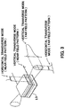
- the laser beams are emitted from the edge portion of the laser device as shown in FIG. 3. Resembling the shape of the edge portion, the spatial power distribution of the emitted laser beams is typically known in the shape of an elongated ellipse with the lengths of the minor and major axes of 0.2 to 40 microns and 80 to 200 microns, respectively.
- the laser beams are focussed using the optical system further to a beam flux having the minor and major axes of 0.5 to 20 microns and 50 to 150 microns, respectively.
- the energy distribution of the beams emitted from the laser device affects the energy distribution after the beam focussing. Further, this distribution along the major axis, in particular, does affect directly the final results of the initialization along the direction perpendicular to disk tracks of the phase-change recording medium.
- the area of the recording medium portion to be initialized are each irradiated at least once and preferably twice or more by the laser beams.
- the focussed beams can irradiate, during the period of one rotation of the disk, over the disk area which amount to the circular length multiplied by the major axis length of the ellipse of about 100 microns which corresponds to the aforementioned energy distribution of the laser beams.
- the disk area can be each irradiated more than once for the initialization.
- the time required for the initialization can be decreased considerably by increasing the distance of the laser displacement.
- the distance of the laser device displacement is selected to be 80 microns with a laser device having the major axis length of beam distribution of 100 microns
- the middle portion having a width of about 60 microns is irradiated once, as shown in FIG. 4A, while the side portions each having a width of about 20 microns are irradiated twice. If the distance of the laser device displacement is selected to be larger than the width at half maximum of the beam distribution, there give rise to the portions which are not irradiated at all, in which no initialization is made in these portions.
- the 20 micron side portion tends to be excessively initialized (i.e., crystallized) and has a larger reflectivity compared to that of the middle portion, thereby resulting in undesirable scatter of trucking signals in the direction perpendicular to the disk tracks.
- the 20 micron side portion is quenched for the time period before the second irradiation corresponding one disk rotation and its reflectivity changes accordingly, the above noted change in the 20 micron side portion after the second laser heating may not be simply twice as much as that of caused by the first irradiation. However, the results described above are still true from practical point of optical disk tracking.
- This shortcoming of disk tracking such as described above is obviated by decreasing a laser power irradiating the side portions, which are irradiated twice as the aforementioned 20 micron side portions on the disk, compared to that irradiating the middle portion, which is irradiated once as the 60 micron middle portion.
- the difference in reflectivity can be decreased between the 20 micron side portions and the 60 micron middle portion.
- dispersion of tracking signals can be decreased and the error rate is thereby considerably decreased in succeeding writing and reading steps of the optical recording medium.
- the following layers were formed in the order recited with a sheet-type sputtering apparatus. These layers were a first dielectric layer having a thickness ranging 65 nanometers to 130 nanometers, a recording layer having a thickness ranging 15 nanometers to 35 nanometers, a second dielectric layer having a thickness ranging 15 nanometers to 45 nanometers, and a reflective/heat-dissipating layer having a thickness ranging 7 nanometers to 180 nanometers.
- a hard coat and an overcoat layer were formed on the surface of the substrate with an ultraviolet curing resin disposed by spin coating, each having a thickness ranging 2 microns to 6 microns and 7 microns to 15 microns, respectively.
- a phase-change optical disk was thus fabricated.
- the optical recording layer was primarily composed of Ag, In, Sb and Te.
- the material ZnS-SiO 2 was used, and for the reflective layer, an aluminum alloy was used.
- Initialization steps were subsequently carried out on the optical disk fabricated as above.
- a semiconductor laser device was used, which was prepared by polishing edge surfaces of at least one of its active layer and reflective layer, substantially perpendicular to the direction of the laser emission, according to the embodiment disclosed herein.
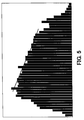
- the spatial energy distribution of the light beams emitted from the semiconductor laser device was found in the shape of an elongated ellipse, as described earlier.
- the width at half maximum is about 101 microns and that the average laser power in the side edge region of the distribution having the width of 10% (i.e., either from 0% to 10% or from 90% to 100%) of the width at half maximum, is from -5% to -10% of the average in the region of the full width at half maximum of the distribution.
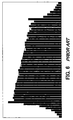
- initialization steps were carried out using a background art semiconductor laser device without polishing edge surfaces.
- the results from the measurements along the major axis of the distribution were obtained as shown in FIG. 6, and the distribution was also found to have the width at half maximum of about 98 microns.
- the average laser power which was found in the side edge region of the distribution having the width of 10% of the width at half maximum is from 0% to +13% of the average in the range of the full width at half maximum of the distribution.
- Another background art semiconductor laser device similar to one used just above was then cured by being energized for 120 hours by its maximum allowable electric power for the blocking test.
- the spatial energy distribution of the light beams emitted from this semiconductor laser device was subsequently measured, the results from the measurements along the major axis of the distribution were obtained as shown in FIG. 7.
- the distance of the laser device displacement (or displacement step) is chosen to be less than 50 microns for a laser device having the major axis length of beam distribution of 100 microns, the entire disk portions are irradiated at least twice. In this case, homogeneous disk quality can be attained by the initialization when it is carried out with relatively low laser power. However, the throughput for the 50 microns displacement distance step is decreased to be less than 50% of that for the 80 microns displacement step.
- a semiconductor laser device fabricated according to the embodiment disclosed herein and an optical system including the laser device are quite useful in use for the optical disk initialization, when the displacement step of ranging 50 microns to 100 microns is adopted for a laser device having the major axis length of beam distribution of 100 microns.
- the spatial distribution of laser power appropriate for the disk initialization is obtained.
- a homogeneous crystallization and concomitant reflectivity of the recording layer in the optical disk, especially in the direction perpendicular to guide tracks can be achieved through initialization steps. Dispersion of tracking signals can thereby be decreased, and the error rate is considerably decreased during writing and reading steps for the optical recording medium.
Landscapes
- Physics & Mathematics (AREA)
- Optics & Photonics (AREA)
- Engineering & Computer Science (AREA)
- Manufacturing & Machinery (AREA)
- Optical Recording Or Reproduction (AREA)
- Manufacturing Optical Record Carriers (AREA)
- Optical Head (AREA)
- Optical Modulation, Optical Deflection, Nonlinear Optics, Optical Demodulation, Optical Logic Elements (AREA)
Applications Claiming Priority (2)
| Application Number | Priority Date | Filing Date | Title |
|---|---|---|---|
| JP36752998 | 1998-12-24 | ||
| JP10367529A JP2000195112A (ja) | 1998-12-24 | 1998-12-24 | 相変化型情報記録媒体の初期化方法 |
Publications (3)
| Publication Number | Publication Date |
|---|---|
| EP1014353A2 true EP1014353A2 (de) | 2000-06-28 |
| EP1014353A3 EP1014353A3 (de) | 2001-08-29 |
| EP1014353B1 EP1014353B1 (de) | 2008-07-16 |
Family
ID=18489543
Family Applications (1)
| Application Number | Title | Priority Date | Filing Date |
|---|---|---|---|
| EP99125824A Expired - Lifetime EP1014353B1 (de) | 1998-12-24 | 1999-12-23 | Initialisierung eines optischen Aufziechnungsmediums des Phasenwechseltyps |
Country Status (6)
| Country | Link |
|---|---|
| US (2) | US6445669B1 (de) |
| EP (1) | EP1014353B1 (de) |
| JP (1) | JP2000195112A (de) |
| AT (1) | ATE401649T1 (de) |
| DE (1) | DE69939098D1 (de) |
| TW (1) | TW455869B (de) |
Cited By (1)
| Publication number | Priority date | Publication date | Assignee | Title |
|---|---|---|---|---|
| FR2813695A1 (fr) * | 2000-09-05 | 2002-03-08 | Moulage Plastique De L Ouest | Procede et dispositif pour l'initialisation d'un milieu d'enregistrement a changement de phase |
Families Citing this family (29)
| Publication number | Priority date | Publication date | Assignee | Title |
|---|---|---|---|---|
| US6600725B1 (en) * | 1998-12-16 | 2003-07-29 | At&T Corp. | Apparatus and method for providing multimedia conferencing services with selective information services |
| US6587429B1 (en) * | 1999-11-16 | 2003-07-01 | Polaroid Corporation | System and method for initializing phase change recording media |
| DE60132380T2 (de) * | 2000-09-28 | 2009-01-02 | Ricoh Co., Ltd. | Optisches Aufzeichnungsmedium, Verfahren zu dessen Herstellung und Verfahren und Vorrichtung zum Aufzeichnen auf oder Lesen von diesem Medium |
| JP2002203343A (ja) * | 2000-10-31 | 2002-07-19 | Matsushita Electric Ind Co Ltd | 光ディスクおよびその製造方法 |
| JP2002237096A (ja) * | 2001-02-09 | 2002-08-23 | Ricoh Co Ltd | 光記録媒体 |
| US7027382B2 (en) | 2001-06-26 | 2006-04-11 | Ricoh Company, Ltd. | Optical recording medium having relation between reflection layer and pit lengths |
| EP1414030A1 (de) * | 2001-07-23 | 2004-04-28 | Sony Corporation | Vorerwärmungs-massenlöschvorrichtung und -verfahren für ein optisches aufzeichnungsmedium und optisches aufzeichnungsmedium |
| CN1410972A (zh) * | 2001-09-25 | 2003-04-16 | 株式会社理光 | 光信息记录媒体,信息消去方法,信息记录方法及装置 |
| CN1290106C (zh) * | 2002-03-07 | 2006-12-13 | 株式会社理光 | 光记录媒体及其制造方法 |
| JP3771859B2 (ja) * | 2002-03-27 | 2006-04-26 | 株式会社リコー | 光情報記録方法及び光情報記録装置 |
| US7063875B2 (en) * | 2002-09-13 | 2006-06-20 | Ricoh Company, Ltd. | Optical recording medium |
| US7351516B2 (en) * | 2002-11-06 | 2008-04-01 | Ricoh Company, Ltd. | Optical information recording medium |
| US7051234B2 (en) * | 2003-02-07 | 2006-05-23 | Dell Products L.P. | Method and system for managing optical storage medium file system structures |
| US6912187B2 (en) * | 2003-02-10 | 2005-06-28 | Dell Products L.P. | Method and system for time compensation of re-writable optical media write parameters |
| US6915374B2 (en) * | 2003-02-19 | 2005-07-05 | Dell Products L.P. | Method and system for setting optical drive write strategies |
| US20040160873A1 (en) * | 2003-02-19 | 2004-08-19 | Pereira David M. | Method and system for creating an optical drive write strategy for an unknown optical media |
| US7483342B2 (en) * | 2003-02-28 | 2009-01-27 | Dell Products L.P. | Method and system for reconditioning optical storage media to write updated information |
| US7161881B2 (en) * | 2003-04-23 | 2007-01-09 | Dell Products L.P. | Method and system for optical drive write strategies embedded in an optical medium |
| JP2005044491A (ja) * | 2003-07-10 | 2005-02-17 | Ricoh Co Ltd | 光記録媒体およびその製造方法 |
| US20050030860A1 (en) * | 2003-08-08 | 2005-02-10 | Gage Donald B. | Method and system for optical medium power calibration |
| EP1515315B1 (de) * | 2003-08-26 | 2007-07-25 | Ricoh Company, Ltd. | Informationsaufzeichnungsverfahren, Informationsaufzeichnungsvorrichtung, optisches Informationsaufzeichnungsmedium, Programm zur Aufzeichnung von Informationen und Speichermedium |
| US7423943B2 (en) * | 2003-10-18 | 2008-09-09 | Dell Products L.P. | Method and system for setting optical drive write speed |
| US7488701B2 (en) | 2004-03-29 | 2009-02-10 | Ricoh Company, Ltd. | Optical information recording medium, manufacturing method thereof and image processing method |
| JP4382646B2 (ja) * | 2004-05-17 | 2009-12-16 | 株式会社リコー | 光記録媒体とその製造方法 |
| US7391694B2 (en) * | 2004-07-07 | 2008-06-24 | Dell Products L.P. | System and method for embedding optical drive compatibility information in optical media |
| US7352670B2 (en) * | 2004-08-02 | 2008-04-01 | Dell Products Lp. | System and method for optical media information storage life tracking |
| US7268796B2 (en) * | 2005-03-21 | 2007-09-11 | Dell Products L.P. | Process and mechanism to label removable media |
| JP2006313077A (ja) * | 2005-05-06 | 2006-11-16 | Ricoh Co Ltd | 光学積層体検査方法,光学積層体製造方法および光学積層体検査装置ならびに光学積層体製造装置 |
| CN104407217B (zh) * | 2014-11-05 | 2017-02-15 | 贝兹维仪器(苏州)有限公司 | 一种应用于电阻率测量仪的usb转接头 |
Family Cites Families (16)
| Publication number | Priority date | Publication date | Assignee | Title |
|---|---|---|---|---|
| JPH0242661A (ja) * | 1988-08-03 | 1990-02-13 | Fuji Electric Co Ltd | 光記録媒体の初期化方法 |
| JPH0434725A (ja) * | 1990-05-30 | 1992-02-05 | Toshiba Corp | 光ディスク装置 |
| JPH04113519A (ja) * | 1990-08-31 | 1992-04-15 | Toray Ind Inc | 光記録媒体の初期化方法 |
| DE69529442T2 (de) * | 1994-09-22 | 2003-11-20 | Ricoh Co., Ltd. | Informationsaufzeichnungsverfahren und -vorrichtung |
| JP2867950B2 (ja) * | 1996-03-15 | 1999-03-10 | 日本電気株式会社 | 光ディスクの初期化装置 |
| JPH09320120A (ja) * | 1996-05-28 | 1997-12-12 | Toray Ind Inc | 記録用ディスクの処理装置および処理方法ならびに記録用ディスクの製造方法 |
| JP3065945B2 (ja) * | 1996-07-08 | 2000-07-17 | 株式会社リコー | 光ディスクの初期化方法及び初期化された光ディスク |
| JP3575183B2 (ja) * | 1996-10-03 | 2004-10-13 | 株式会社日立製作所 | 光学的情報記録媒体とその初期化方法および初期化装置 |
| JPH10172145A (ja) * | 1996-12-13 | 1998-06-26 | Nec Corp | 相変化光ディスクの初期化装置 |
| US5875160A (en) * | 1996-12-14 | 1999-02-23 | Ricoh Company, Ltd. | Method and device for initializing optical recording medium of phase change type, and optical recording medium |
| JPH10208310A (ja) * | 1997-01-17 | 1998-08-07 | Ricoh Co Ltd | 相変化型光記録媒体の初期化方法 |
| JPH10198959A (ja) * | 1997-01-10 | 1998-07-31 | Sony Corp | 相変化光ディスクの初期化方法及び相変化光ディスク |
| JPH10241160A (ja) * | 1997-02-21 | 1998-09-11 | Nec Corp | 相変化記録媒体の初期化方法 |
| JPH10312582A (ja) * | 1997-05-13 | 1998-11-24 | Matsushita Electric Ind Co Ltd | 光学的情報記録担体の初期化装置 |
| US5974025A (en) * | 1997-08-15 | 1999-10-26 | Ricoh Company, Ltd. | Optical recording medium and recording and reproducing method using the same |
| JP3302919B2 (ja) * | 1997-11-27 | 2002-07-15 | 株式会社リコー | 光記録媒体の初期化方法及び初期化装置 |
-
1998
- 1998-12-24 JP JP10367529A patent/JP2000195112A/ja active Pending
-
1999
- 1999-12-23 TW TW088122812A patent/TW455869B/zh not_active IP Right Cessation
- 1999-12-23 US US09/471,345 patent/US6445669B1/en not_active Ceased
- 1999-12-23 AT AT99125824T patent/ATE401649T1/de not_active IP Right Cessation
- 1999-12-23 EP EP99125824A patent/EP1014353B1/de not_active Expired - Lifetime
- 1999-12-23 DE DE69939098T patent/DE69939098D1/de not_active Expired - Lifetime
-
2004
- 2004-04-14 US US10/825,441 patent/USRE39901E1/en not_active Expired - Lifetime
Cited By (2)
| Publication number | Priority date | Publication date | Assignee | Title |
|---|---|---|---|---|
| FR2813695A1 (fr) * | 2000-09-05 | 2002-03-08 | Moulage Plastique De L Ouest | Procede et dispositif pour l'initialisation d'un milieu d'enregistrement a changement de phase |
| WO2002021521A1 (fr) * | 2000-09-05 | 2002-03-14 | Moulage Plastique De L'ouest | Procede et dispositif pour l'initialisation d'un milieu d'enregistrement a changement de phase |
Also Published As
| Publication number | Publication date |
|---|---|
| EP1014353A3 (de) | 2001-08-29 |
| ATE401649T1 (de) | 2008-08-15 |
| DE69939098D1 (de) | 2008-08-28 |
| USRE39901E1 (en) | 2007-10-30 |
| EP1014353B1 (de) | 2008-07-16 |
| TW455869B (en) | 2001-09-21 |
| US6445669B1 (en) | 2002-09-03 |
| JP2000195112A (ja) | 2000-07-14 |
Similar Documents
| Publication | Publication Date | Title |
|---|---|---|
| EP1014353B1 (de) | Initialisierung eines optischen Aufziechnungsmediums des Phasenwechseltyps | |
| US5255260A (en) | Optical recording apparatus employing stacked recording media with spiral grooves and floating optical heads | |
| US6990053B2 (en) | Method and apparatus for initializing optical recording media | |
| CN1200700A (zh) | 光学信息记录媒体及其制造方法、光学信息记录、再生方法及光学信息记录、再生装置 | |
| JP2785763B2 (ja) | 相変化光ディスク | |
| US5521901A (en) | Re-writable phase change type optical disk with suppressed recording mark distortion | |
| US7482109B2 (en) | Optical information recording medium | |
| JPH07105574A (ja) | 光情報記録媒体 | |
| JP2002304738A (ja) | 相変化型光ディスクの初期化方法 | |
| JP2003272172A (ja) | 光ディスク初期化方法及び初期化装置 | |
| JP2892818B2 (ja) | 記録媒体の初期化方法 | |
| JP3886634B2 (ja) | 情報の記録媒体の初期化方法及び初期化装置 | |
| JPH04216323A (ja) | 光記録媒体の製造方法 | |
| JP2006252765A (ja) | 相変化型情報記録媒体 | |
| JP3214183B2 (ja) | 光学的情報記録媒体 | |
| JP2000298874A (ja) | 相変化型光ディスク及びその製造方法 | |
| JPH1021580A (ja) | 光記録媒体およびその製造方法 | |
| JP3523799B2 (ja) | 相変化記録媒体 | |
| JPH09212918A (ja) | 情報の記録媒体とその初期化方法及び初期化装置 | |
| KR19980024772A (ko) | 상 변화형 광 기록 매체 및 광 기록 매체에 광학적으로 기록하는 방법 | |
| JPH10106045A (ja) | 光記録媒体とその製造方法および製造装置 | |
| JPWO1997032304A1 (ja) | 相変化型光記録媒体の設計方法および相変化型光記録媒体 | |
| JPH11120594A (ja) | 光ディスクの初期化方法及び光ディスクの初期化装置 | |
| JP2004001353A (ja) | 相変化型記録媒体、その記録方法および記録装置 | |
| JP2002245679A (ja) | 光情報記録媒体、その初期化方法及び初期化装置 |
Legal Events
| Date | Code | Title | Description |
|---|---|---|---|
| PUAI | Public reference made under article 153(3) epc to a published international application that has entered the european phase |
Free format text: ORIGINAL CODE: 0009012 |
|
| AK | Designated contracting states |
Kind code of ref document: A2 Designated state(s): AT BE CH CY DE DK ES FI FR GB GR IE IT LI LU MC NL PT SE |
|
| AX | Request for extension of the european patent |
Free format text: AL;LT;LV;MK;RO;SI |
|
| PUAL | Search report despatched |
Free format text: ORIGINAL CODE: 0009013 |
|
| AK | Designated contracting states |
Kind code of ref document: A3 Designated state(s): AT BE CH CY DE DK ES FI FR GB GR IE IT LI LU MC NL PT SE |
|
| AX | Request for extension of the european patent |
Free format text: AL;LT;LV;MK;RO;SI |
|
| 17P | Request for examination filed |
Effective date: 20020228 |
|
| AKX | Designation fees paid |
Free format text: AT BE CH CY DE DK ES FI FR GB GR IE IT LI LU MC NL PT SE |
|
| RAP1 | Party data changed (applicant data changed or rights of an application transferred) |
Owner name: RICOH COMPANY LTD. |
|
| 17Q | First examination report despatched |
Effective date: 20050322 |
|
| 17Q | First examination report despatched |
Effective date: 20050322 |
|
| GRAP | Despatch of communication of intention to grant a patent |
Free format text: ORIGINAL CODE: EPIDOSNIGR1 |
|
| GRAS | Grant fee paid |
Free format text: ORIGINAL CODE: EPIDOSNIGR3 |
|
| GRAA | (expected) grant |
Free format text: ORIGINAL CODE: 0009210 |
|
| AK | Designated contracting states |
Kind code of ref document: B1 Designated state(s): AT BE CH CY DE DK ES FI FR GB GR IE IT LI LU MC NL PT SE |
|
| REG | Reference to a national code |
Ref country code: GB Ref legal event code: FG4D |
|
| REG | Reference to a national code |
Ref country code: CH Ref legal event code: EP |
|
| REF | Corresponds to: |
Ref document number: 69939098 Country of ref document: DE Date of ref document: 20080828 Kind code of ref document: P |
|
| REG | Reference to a national code |
Ref country code: IE Ref legal event code: FG4D |
|
| NLV1 | Nl: lapsed or annulled due to failure to fulfill the requirements of art. 29p and 29m of the patents act | ||
| PG25 | Lapsed in a contracting state [announced via postgrant information from national office to epo] |
Ref country code: PT Free format text: LAPSE BECAUSE OF FAILURE TO SUBMIT A TRANSLATION OF THE DESCRIPTION OR TO PAY THE FEE WITHIN THE PRESCRIBED TIME-LIMIT Effective date: 20081216 Ref country code: NL Free format text: LAPSE BECAUSE OF FAILURE TO SUBMIT A TRANSLATION OF THE DESCRIPTION OR TO PAY THE FEE WITHIN THE PRESCRIBED TIME-LIMIT Effective date: 20080716 Ref country code: ES Free format text: LAPSE BECAUSE OF FAILURE TO SUBMIT A TRANSLATION OF THE DESCRIPTION OR TO PAY THE FEE WITHIN THE PRESCRIBED TIME-LIMIT Effective date: 20081027 |
|
| PG25 | Lapsed in a contracting state [announced via postgrant information from national office to epo] |
Ref country code: FI Free format text: LAPSE BECAUSE OF FAILURE TO SUBMIT A TRANSLATION OF THE DESCRIPTION OR TO PAY THE FEE WITHIN THE PRESCRIBED TIME-LIMIT Effective date: 20080716 Ref country code: AT Free format text: LAPSE BECAUSE OF FAILURE TO SUBMIT A TRANSLATION OF THE DESCRIPTION OR TO PAY THE FEE WITHIN THE PRESCRIBED TIME-LIMIT Effective date: 20080716 |
|
| PG25 | Lapsed in a contracting state [announced via postgrant information from national office to epo] |
Ref country code: BE Free format text: LAPSE BECAUSE OF FAILURE TO SUBMIT A TRANSLATION OF THE DESCRIPTION OR TO PAY THE FEE WITHIN THE PRESCRIBED TIME-LIMIT Effective date: 20080716 |
|
| PG25 | Lapsed in a contracting state [announced via postgrant information from national office to epo] |
Ref country code: DK Free format text: LAPSE BECAUSE OF FAILURE TO SUBMIT A TRANSLATION OF THE DESCRIPTION OR TO PAY THE FEE WITHIN THE PRESCRIBED TIME-LIMIT Effective date: 20080716 |
|
| PLBE | No opposition filed within time limit |
Free format text: ORIGINAL CODE: 0009261 |
|
| STAA | Information on the status of an ep patent application or granted ep patent |
Free format text: STATUS: NO OPPOSITION FILED WITHIN TIME LIMIT |
|
| 26N | No opposition filed |
Effective date: 20090417 |
|
| PG25 | Lapsed in a contracting state [announced via postgrant information from national office to epo] |
Ref country code: MC Free format text: LAPSE BECAUSE OF NON-PAYMENT OF DUE FEES Effective date: 20081231 |
|
| REG | Reference to a national code |
Ref country code: CH Ref legal event code: PL |
|
| PG25 | Lapsed in a contracting state [announced via postgrant information from national office to epo] |
Ref country code: IT Free format text: LAPSE BECAUSE OF FAILURE TO SUBMIT A TRANSLATION OF THE DESCRIPTION OR TO PAY THE FEE WITHIN THE PRESCRIBED TIME-LIMIT Effective date: 20080716 |
|
| PG25 | Lapsed in a contracting state [announced via postgrant information from national office to epo] |
Ref country code: LI Free format text: LAPSE BECAUSE OF NON-PAYMENT OF DUE FEES Effective date: 20081231 Ref country code: IE Free format text: LAPSE BECAUSE OF NON-PAYMENT OF DUE FEES Effective date: 20081223 Ref country code: CH Free format text: LAPSE BECAUSE OF NON-PAYMENT OF DUE FEES Effective date: 20081231 |
|
| PG25 | Lapsed in a contracting state [announced via postgrant information from national office to epo] |
Ref country code: SE Free format text: LAPSE BECAUSE OF FAILURE TO SUBMIT A TRANSLATION OF THE DESCRIPTION OR TO PAY THE FEE WITHIN THE PRESCRIBED TIME-LIMIT Effective date: 20081016 |
|
| PG25 | Lapsed in a contracting state [announced via postgrant information from national office to epo] |
Ref country code: LU Free format text: LAPSE BECAUSE OF NON-PAYMENT OF DUE FEES Effective date: 20081223 |
|
| PG25 | Lapsed in a contracting state [announced via postgrant information from national office to epo] |
Ref country code: CY Free format text: LAPSE BECAUSE OF FAILURE TO SUBMIT A TRANSLATION OF THE DESCRIPTION OR TO PAY THE FEE WITHIN THE PRESCRIBED TIME-LIMIT Effective date: 20080716 |
|
| PG25 | Lapsed in a contracting state [announced via postgrant information from national office to epo] |
Ref country code: GR Free format text: LAPSE BECAUSE OF FAILURE TO SUBMIT A TRANSLATION OF THE DESCRIPTION OR TO PAY THE FEE WITHIN THE PRESCRIBED TIME-LIMIT Effective date: 20081017 |
|
| REG | Reference to a national code |
Ref country code: DE Ref legal event code: R082 Ref document number: 69939098 Country of ref document: DE Representative=s name: MEISSNER, BOLTE & PARTNER GBR, DE |
|
| PGFP | Annual fee paid to national office [announced via postgrant information from national office to epo] |
Ref country code: DE Payment date: 20131220 Year of fee payment: 15 Ref country code: GB Payment date: 20131219 Year of fee payment: 15 |
|
| REG | Reference to a national code |
Ref country code: DE Ref legal event code: R082 Ref document number: 69939098 Country of ref document: DE Representative=s name: MEISSNER, BOLTE & PARTNER GBR, DE |
|
| PGFP | Annual fee paid to national office [announced via postgrant information from national office to epo] |
Ref country code: FR Payment date: 20131220 Year of fee payment: 15 |
|
| REG | Reference to a national code |
Ref country code: DE Ref legal event code: R119 Ref document number: 69939098 Country of ref document: DE |
|
| GBPC | Gb: european patent ceased through non-payment of renewal fee |
Effective date: 20141223 |
|
| REG | Reference to a national code |
Ref country code: FR Ref legal event code: ST Effective date: 20150831 |
|
| PG25 | Lapsed in a contracting state [announced via postgrant information from national office to epo] |
Ref country code: GB Free format text: LAPSE BECAUSE OF NON-PAYMENT OF DUE FEES Effective date: 20141223 Ref country code: DE Free format text: LAPSE BECAUSE OF NON-PAYMENT OF DUE FEES Effective date: 20150701 |
|
| PG25 | Lapsed in a contracting state [announced via postgrant information from national office to epo] |
Ref country code: FR Free format text: LAPSE BECAUSE OF NON-PAYMENT OF DUE FEES Effective date: 20141231 |