EP1018567A2 - Procédé de fabrication des objets autoportants - Google Patents
Procédé de fabrication des objets autoportants Download PDFInfo
- Publication number
- EP1018567A2 EP1018567A2 EP99310402A EP99310402A EP1018567A2 EP 1018567 A2 EP1018567 A2 EP 1018567A2 EP 99310402 A EP99310402 A EP 99310402A EP 99310402 A EP99310402 A EP 99310402A EP 1018567 A2 EP1018567 A2 EP 1018567A2
- Authority
- EP
- European Patent Office
- Prior art keywords
- substrate
- linear suspension
- solid
- suspension supports
- deposit
- Prior art date
- Legal status (The legal status is an assumption and is not a legal conclusion. Google has not performed a legal analysis and makes no representation as to the accuracy of the status listed.)
- Granted
Links
Images

Classifications
-
- C—CHEMISTRY; METALLURGY
- C23—COATING METALLIC MATERIAL; COATING MATERIAL WITH METALLIC MATERIAL; CHEMICAL SURFACE TREATMENT; DIFFUSION TREATMENT OF METALLIC MATERIAL; COATING BY VACUUM EVAPORATION, BY SPUTTERING, BY ION IMPLANTATION OR BY CHEMICAL VAPOUR DEPOSITION, IN GENERAL; INHIBITING CORROSION OF METALLIC MATERIAL OR INCRUSTATION IN GENERAL
- C23C—COATING METALLIC MATERIAL; COATING MATERIAL WITH METALLIC MATERIAL; SURFACE TREATMENT OF METALLIC MATERIAL BY DIFFUSION INTO THE SURFACE, BY CHEMICAL CONVERSION OR SUBSTITUTION; COATING BY VACUUM EVAPORATION, BY SPUTTERING, BY ION IMPLANTATION OR BY CHEMICAL VAPOUR DEPOSITION, IN GENERAL
- C23C16/00—Chemical coating by decomposition of gaseous compounds, without leaving reaction products of surface material in the coating, i.e. chemical vapour deposition [CVD] processes
- C23C16/01—Chemical coating by decomposition of gaseous compounds, without leaving reaction products of surface material in the coating, i.e. chemical vapour deposition [CVD] processes on temporary substrates, e.g. substrates subsequently removed by etching
-
- C—CHEMISTRY; METALLURGY
- C23—COATING METALLIC MATERIAL; COATING MATERIAL WITH METALLIC MATERIAL; CHEMICAL SURFACE TREATMENT; DIFFUSION TREATMENT OF METALLIC MATERIAL; COATING BY VACUUM EVAPORATION, BY SPUTTERING, BY ION IMPLANTATION OR BY CHEMICAL VAPOUR DEPOSITION, IN GENERAL; INHIBITING CORROSION OF METALLIC MATERIAL OR INCRUSTATION IN GENERAL
- C23C—COATING METALLIC MATERIAL; COATING MATERIAL WITH METALLIC MATERIAL; SURFACE TREATMENT OF METALLIC MATERIAL BY DIFFUSION INTO THE SURFACE, BY CHEMICAL CONVERSION OR SUBSTITUTION; COATING BY VACUUM EVAPORATION, BY SPUTTERING, BY ION IMPLANTATION OR BY CHEMICAL VAPOUR DEPOSITION, IN GENERAL
- C23C16/00—Chemical coating by decomposition of gaseous compounds, without leaving reaction products of surface material in the coating, i.e. chemical vapour deposition [CVD] processes
- C23C16/44—Chemical coating by decomposition of gaseous compounds, without leaving reaction products of surface material in the coating, i.e. chemical vapour deposition [CVD] processes characterised by the method of coating
- C23C16/4418—Methods for making free-standing articles
-
- C—CHEMISTRY; METALLURGY
- C23—COATING METALLIC MATERIAL; COATING MATERIAL WITH METALLIC MATERIAL; CHEMICAL SURFACE TREATMENT; DIFFUSION TREATMENT OF METALLIC MATERIAL; COATING BY VACUUM EVAPORATION, BY SPUTTERING, BY ION IMPLANTATION OR BY CHEMICAL VAPOUR DEPOSITION, IN GENERAL; INHIBITING CORROSION OF METALLIC MATERIAL OR INCRUSTATION IN GENERAL
- C23C—COATING METALLIC MATERIAL; COATING MATERIAL WITH METALLIC MATERIAL; SURFACE TREATMENT OF METALLIC MATERIAL BY DIFFUSION INTO THE SURFACE, BY CHEMICAL CONVERSION OR SUBSTITUTION; COATING BY VACUUM EVAPORATION, BY SPUTTERING, BY ION IMPLANTATION OR BY CHEMICAL VAPOUR DEPOSITION, IN GENERAL
- C23C16/00—Chemical coating by decomposition of gaseous compounds, without leaving reaction products of surface material in the coating, i.e. chemical vapour deposition [CVD] processes
- C23C16/44—Chemical coating by decomposition of gaseous compounds, without leaving reaction products of surface material in the coating, i.e. chemical vapour deposition [CVD] processes characterised by the method of coating
- C23C16/458—Chemical coating by decomposition of gaseous compounds, without leaving reaction products of surface material in the coating, i.e. chemical vapour deposition [CVD] processes characterised by the method of coating characterised by the method used for supporting substrates in the reaction chamber
Definitions
- CVD chemical vapor deposition
- NPS near-net shape
- the present invention provides an improved method of mounting substrates during the CVD process. It is particularly applicable to the production of near-net shape silicon carbide articles.
- Free-standing silicon carbide materials produced by CVD processing in applications requiring a high degree of surface smoothness and polishability are described in U.S. Patent No. 5,374,412. Apparatus and process conditions used to produce such articles are described in that patent.
- U.S. Patent Nos. 4,990,374; 4,997,678 and 5,071,596 further describe CVD processes for producing free-standing silicon carbide materials by the pyrolytic deposit of SiC on a mandrel.
- CVD derived articles are produced by CVD deposit of the desired material on a substrate, followed by separation of the article from the substrate.
- One prior method produces a relatively large sheet of monolithic SiC on a flat graphite mandrel coated with a thin layer of a release coating. Pyrolysis of methyltrichlorosilane in argon and excess hydrogen produced a deposit which, after separation from the mandrel, was cut into multiple susceptor rings for use supporting wafers in semiconductor processing furnaces. While this method produces satisfactory parts, they are not produced in near-net shape and require substantial machining. The production of the deposit in near-net shape is desirable to reduce the amount of waste material generated and reduce the amount of machining required.
- Another prior technique controls the deposition by providing a channel surrounding that portion or zone of the substrate surface where the deposit is desired.
- the channel functions to restrict flow of the reactive deposition gases to the substrate surfaces surrounding the deposition zone whereby any deposit on the surrounding surfaces is substantially thinner than the deposit formed in the deposition zone.
- Still another previous method provided multiple shaped graphite ring mandrels (substrates) mounted along the extent of the deposition chamber by detachable graphite mounts gripping the edge of the rings.
- Silicon carbide was deposited on both sides of the mandrels, the mandrels removed from the deposition chamber and the edges of the deposits on the mandrels machined to release the bottom and top deposits as two separate silicon carbide articles.
- This process resulted in relatively heavy deposits of silicon carbide bridging the graphite mandrel and the graphite mounts, necessitating difficult machining in the vicinity of the areas occupied by the mounts, and often resulted in cracks developing in the deposits during separation of the mount from the mandrel. These cracks often propagated through the desired product causing it to be rejected. If sufficient mounts are not used, the increased weight of the deposit on the mandrels sometimes caused the mandrels to slip from the mounts damaging the deposits and adjacent mandrels.
- Chemical vapor deposition has been used to produce both free-standing articles and coatings of various materials, such as, silicon carbide.
- CVD Chemical vapor deposition
- Such a process involves reacting vaporized or gaseous chemical precursors in the vicinity of a substrate to result in silicon carbide depositing on the substrate. The deposition reaction is continued until the deposit reaches the desired thickness.
- the substrate is the article to be coated and the coating is relatively thin, generally less than 100 microns (0.1mm) thick.
- a thicker deposit generally greater than 0.1 mm thick, is formed as a shell on the substrate and then separated from the substrate to provide the silicon carbide article.
- silicon carbide precursor gases or vapors are fed to a deposition chamber where they are heated to a temperature at which they react producing silicon carbide.
- the silicon carbide deposits as a shell on a solid substrate.
- the deposition is continued until the desired thickness of silicon carbide is deposited.
- the substrate is then removed from the deposition chamber and the shell separated therefrom.
- Monolithic silicon carbide plates and cylinders have been produced by applying such chemical vapor deposition (CVD) techniques on suitably shaped substrates.
- silicon carbide precursor gases or vapors are brought to the appropriate conditions to cause them to react, they produce silicon carbide which deposits on any available surface.
- Such deposit generally is not limited to the intended surface of the substrate and generally extends past such surface to adjoining surfaces as well as depositing on the walls, housing and any other available surfaces associated with the deposition chamber.
- the silicon carbide deposit has extended past the dimensional limits of the substrate covering adjacent portions of the support structure holding or clamping the mandrel/substrate in position in the deposition chamber.
- the present invention is directed to a process, and associated apparatus, for producing bulk materials by chemical vapor deposition wherein extraneous deposits (i.e. deposits formed on deposition chamber surfaces other than the intended production surface of the substrate) are minimized. Reduction of such extraneous deposits provides economic benefits both with respect to the cost of raw materials and the labor costs associated with CVD processing.
- the present invention further provides a relatively inexpensive method of mounting the substrate in the deposition chamber whereby the substrate can be readily separated from the mounting structure without causing cracks to propagate through the deposited bulk material.
- a further advantage of the inventive process is the use of devices to mount the substrate which are sufficiently inexpensive to be disposable, whereby the removal of extraneous material deposited thereon is not necessary.
- the inventive process can be used to produce articles of silicon carbide or of any of the materials which are capable of being produced by CVD processing, such as zinc sulfide, zinc selenide, boron nitride, boron carbide, silicon nitride, titanium diboride and aluminum nitride.
- linear suspension supports preferably flexible linear suspension supports, such as ropes or cables, which engage the substrate(s) at their edge(s) and extend to supporting structure on, or in, the deposition chamber housing.
- the suspension supports are referred to as linear because they have a longitudinal dimension which is much greater than their transverse dimension which is located adjacent the substrate.
- the linear suspension supports and the substrates are designed to enable minimal contact between the surface of the substrate and any other apparatus in the deposition zone, while providing adequate support to assure that the substrate does not break loose as it gains weight during the deposition process.
- any deposits formed on the preferred rope or cable linear supports can often be removed by merely flexing the rope or cable. Should the linear suspension supports become unduly coated or contaminated in some other manner, they are relatively inexpensive to replace, and therefore do not require extensive cleaning or decontamination procedures to enable them to be reused.
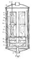
- Figure 1 is a schematic cross-section of a CVD furnace in which the present invention is practiced.
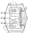
- Figure 2 is a cross-section of one of the deposition boxes illustrated in the furnace of Figure 1.
- Figure 3 is a top view of a cross-section of the deposition box illustrated in Figure 2.
- Figure 4 is a schematic cross-section of a further CVD furnace in which several embodiments of the present invention are being practiced.
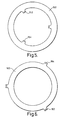
- Figure 5 is a top view of a substrate particularly adapted for use in the present invention.
- Figure 6 is a top view of a further substrate particularly adapted for use in the present invention.
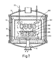
- Figure 7 is a schematic cross-section of a further CVD furnace in which several further embodiments of the present invention are being practiced.
- a preferred CVD furnace for practicing the present invention is illustrated in Figure 1.
- the furnace 10 encloses multiple deposition boxes 12, 14, 16 and 18. As most fully illustrated in deposition boxes 12 and 14, multiple flat ring-like mandrels, or substrates, 20, are deployed along the length of the box.
- Precursor reactive gases are fed to the upper box 12 through injector 22.
- the precursor reactive gases circulate around and through the substrates, eventually passing to lower deposition box 14 where they similarly circulate about the substrates deployed in that box.
- the gases eventually pass from deposition box 14 through end plate 23, exhaust plate 24, pass through the flow diversion plate 26, around baffle plate 28 and eventually are discharged from the furnace through exhaust port 30.
- Heating elements 32, 34 for controlling the deposition temperature are provided outside of the deposition boxes.
- Insulation 36, 38 is provided between the furnace wall and the heating elements. Substrates and an injector may be deployed with deposition boxes 16 and 18 in the same manner as shown with deposition boxes 12 and 14, or, alternatively, different substrates may be deployed and supported in a different manner in boxes 16 and 18.
- Deposition box 12 is further illustrated in Figures 2 and 3.
- the three walls 50, 52 and 54, of the box are connected through three corner posts 56, 58 and 60.
- Cover plate 62 contains port 64 which cooperates with injector 22 to essentially preclude the reactive gases migrating into the remainder of the furnace from the deposition box.
- a mating ring 66 provides a conforming mating relationship between upper deposition box 12 and lower deposition box 14.
- Three linear suspension supports 68 extend from anchoring means associated with the cover plate 62, through an engagement with each of the eight ring-like substrates 20, to further anchoring means associated with mating ring 66.
- the linear suspension supports 68 provided in the lower deposition box 14 ( Figure 1) are attached to anchoring supports associated with the mating ring 66 and end plate 23.
- the linear suspension supports 68 are designated to be linear because their dimension which is spanned by contact with the substrate, usually their diameter, is minor in relation to their longitudinal dimension, or length.
- the linear suspension supports are sufficiently manually flexible to be coilable.
- Such preferred supports can be selected from rope, cable or wires.
- the supports need to be made of materials which will withstand the temperatures and chemicals encountered during the deposition process. Representative suitable materials include graphite, sapphire, tungsten, molybdenum and quartz. We have found braided graphite rope to form particularly suitable linear suspension supports for the production of CVD silicon carbide articles in a deposition box arrangement similar to that shown in Figures 1-3.
- the anchoring means for securing the linear suspension supports can be any means capable of holding, or anchoring, the ends of such supports in place throughout the deposition process.
- Suitable anchoring means provided on the cover plate, walls or posts of the deposition box include hooks, eyebolts, cleats, via holes, or specialized mating means which cooperate with specialized mating means at the ends of the suspension supports.
- the linear suspension supports engage the substrates in a supporting relationship.
- the engagement does not result in a rigid fixed joinder between the supports and the substrates such as would be provided by a locking clamp, but instead permits a limited degree of movement between the support and the substrate.
- Engaging the linear suspension supports in slots or holes provided at the periphery of the substrates and fixing an interfering structure projecting from the supports beneath the slot or hole are preferred forms of supporting the substrates when they are deployed in a generally horizontal configuration, as in Figures 1-3.
- the interfering structure can be a knot tied in a rope or cable support, or it could be a pin or screw laterally attached to a rope, wire or cable support or it could be the residue of a hardened cement.
- Figure 4 is a schematic of several different shaped substrates supported in a single deposition box 69 in a furnace 70 of a CVD system by linear suspension supports in accord with the present invention.
- the substrates also referred to as mandrels, are typically fabricated from relatively thin material with one, two, or multiple sides, having a figure, or shape, which is a negative of the actual article to be produced.
- the substrates can be fabricated from materials such as graphite, silicon, sapphire, quartz, molybdenum, titanium or tantalum.
- the same item numbers are used to designate components similar to those of the Figure 1-3 embodiment.
- Substrate 71 is a hollow shape, such as a cylindrical tube or box channel, which engages two or more linear suspension supports 72, 74 at its upper periphery.
- the two or more linear suspension supports 72, 74 are joined at 76 to form a further support 78 which extends upwardly to functional attachment to a rotation means, such as motor 80.
- the further support 78 is shielded by an insulated housing 82 extending from the roof of the furnace 70 to the deposition box 69. Rotation of the substrate throughout the deposition process can, in some cases, provide a more uniform deposition.
- Substrate 90 is a plate containing a dome shaped portion 92. This substrate is supported by two linear suspension supports 94, 96 descending from the top of the deposition box 69, and two similar linear supports 98, 100 extending up from the floor of the deposition box.
- Substrate 110 is for the production of cone-shaped articles. It is suspended by a single linear suspension support 112 anchored to the roof of the deposition box and two linear supports 114, 116 anchored to the floor of the box.
- Substrate 120 is a ring-shaped plate, or disc, similar to the substrates 20 used in the Figure 1 embodiment.
- Substrate 130 is a flat plate. Both substrates 120 and 130 are suspended vertically in similar manner by two linear suspension supports anchored to the roof of the deposition box and engaging the periphery of the substrates. Two linear supports, which are anchored to the floor of the deposition box, also engage the periphery of each of the substrates.
- the horizontally suspended series of ring-shaped substrates 20 and linear suspension supports 68 shown in Figure 4 are similar to the like-numbered substrates and supports in the Figure 1 embodiment.
- Susceptor rings for supporting wafers in semiconductor furnaces have been produced of CVD silicon carbide in a furnace similar to the embodiment of Figures 1-3.
- Eight 0.1 inch thick graphite ring mandrels 20 having an outside diameter of 9.75 inches and an inside diameter of 6.25 inches were suspended in a deposition box 12 on three graphite rope linear suspension supports 68. Three holes were drilled in each ring near the periphery of its inner diameter.
- Four of the rings were coated with an amorphous carbon release layer.
- the graphite ropes were inserted in the holes and knots were tied in the rope to support and fix the location of each ring.
- the graphite ropes were tied to the top and bottom covers of the triangular deposition box to horizontally suspend the rings four inches apart.
- a precursor gas mixture of methyltrichlorosilane in excess hydrogen and argon was fed to the top of the deposition box and silicon carbide was deposited for approximately 75 hours at a temperature of 1350°C and a pressure of 200 torr.
- the flow rate of methyltrichlorosilane varied between 9 and 12 standard liters per minute (slpm), the flow rate of H 2 was 67 slpm and that of Ar was 69 slpm.
- the silicon carbide deposited on both sides of the rings to thicknesses in the range of 0.11 to 0.25 inches with no apparent visible cracks or chipping of the deposits on the rings.
- the graphite rope suspension supports were released from the top and bottom covers of the box, and removed, with the rings, from the box.
- the graphite was removed by burning in air at 700°C. Separation of the substrate from the deposits on each side thereof resulted in the production of two silicon carbide rings for each graphite mandrel. The resulting silicon carbide rings were then machined to the dimensions required of susceptor rings used in semiconductor furnaces.
- Mandrel 150 of Figure 5 is essentially ring-shaped, however protrusions, or tabs 152, which extend from the inner nominal diameter of the ring toward its center, are spaced about the ring's inner periphery. A tab is provided for each of the linear suspension supports used to suspend the mandrel in the deposition zone.
- An engagement means such as slot 154, capable of engaging the linear suspension support, is provided on each of the tabs.
- the mandrels are attached to the linear suspension supports by the engagement means during the deposition. Upon completion of the deposition, less machining is required to remove the tabs and form the article in its final shape than is required with the Figure 1-3 mandrels.
- the mandrel 160 of Figure 6 is generally ring-shaped with protrusions, or tabs 162, extending outwardly from its outer nominal diameter/periphery. Each tab contains an engagement means, such as slot 164, for engagement with a linear suspension support. As with mandrel 150 ( Figure 5), less machining is required to remove the tabs 162 and finish the article to its final shape than is required with the mandrel 20 ( Figures 1-3).
- Protrusions, or tabs, containing engagement means can be provided on mandrels of various shapes. For instance, they can be provided on the edges of flat plate substrates, such as substrate 130 ( Figure 4), or on the side of three dimensional shaped substrates, such as substrate 90 ( Figure 4). Preferably, depending on the substrate's weight, shape and size, one to four tabs are provided on each substrate. Usually the tabs are removed following the deposition to expose the underlying substrate and to form the article in its final shape.
- linear suspension supports of the preceding embodiments are provided in a generally vertical arrangement.
- Linear suspension supports can also be provided in a generally horizontal arrangement.
- Figure 7 illustrates the use of two generally horizontal arrangements of linear suspension supports according to the present invention. The same item numbers are used to designate components which are similar to those of previous embodiments.
- Each of two flexible linear suspension supports, such as graphite ropes 180 are attached at opposite sides of the deposition box 69.
- the flexible linear suspension supports 180 extend generally horizontally across the chamber and engage a line of four ring-like mandrels 182 through holes provided in the mandrels to vertically suspend the mandrels in the furnace.
- a further linear suspension support 184 suspends another line of four ring-like mandrels 186.
- the linear suspension support 184 is formed from relatively rigid material such as bars, pipes or rods of graphite, molybdenum, tungsten, etc.
- the rigid linear suspension support 184 can be mounted to extend out from both sides of a central post 188, as shown. Alternatively, it can be mounted on two or more posts or it can extend between mounting brackets affixed to opposite side walls 190 of the deposition box.
- One or multiple linear suspension supports 180, 184 may be provided to support each line of substrates.
- the substrates' means for engaging the linear suspension supports may be provided on projections, or tabs.
- those substrates which have an interior void, such as the ring-like mandrels 186, can be suspended in the deposition zone, without the need for additional engagement structure, by hanging them on a linear suspension support extending through the void.
- the described technique of suspending relatively thin substrates in a CVD furnace enables the production of near-net shape, crack-free, CVD free-standing articles in high yield. Moreover, it accomplishes such with substantial reduction in manufacturing costs over the previously used substrate mounting techniques. These reduced manufacturing costs result from:
Landscapes
- Chemical & Material Sciences (AREA)
- General Chemical & Material Sciences (AREA)
- Chemical Kinetics & Catalysis (AREA)
- Engineering & Computer Science (AREA)
- Materials Engineering (AREA)
- Mechanical Engineering (AREA)
- Metallurgy (AREA)
- Organic Chemistry (AREA)
- Chemical Vapour Deposition (AREA)
- Physical Or Chemical Processes And Apparatus (AREA)
Applications Claiming Priority (2)
| Application Number | Priority Date | Filing Date | Title |
|---|---|---|---|
| US09/226,534 US6464912B1 (en) | 1999-01-06 | 1999-01-06 | Method for producing near-net shape free standing articles by chemical vapor deposition |
| US226534 | 1999-01-06 |
Publications (3)
| Publication Number | Publication Date |
|---|---|
| EP1018567A2 true EP1018567A2 (fr) | 2000-07-12 |
| EP1018567A3 EP1018567A3 (fr) | 2000-09-20 |
| EP1018567B1 EP1018567B1 (fr) | 2003-07-23 |
Family
ID=22849304
Family Applications (1)
| Application Number | Title | Priority Date | Filing Date |
|---|---|---|---|
| EP99310402A Expired - Lifetime EP1018567B1 (fr) | 1999-01-06 | 1999-12-22 | Procédé de fabrication des objets autoportants |
Country Status (5)
| Country | Link |
|---|---|
| US (2) | US6464912B1 (fr) |
| EP (1) | EP1018567B1 (fr) |
| JP (1) | JP4619473B2 (fr) |
| DE (1) | DE69909730T2 (fr) |
| IL (1) | IL133765A0 (fr) |
Cited By (2)
| Publication number | Priority date | Publication date | Assignee | Title |
|---|---|---|---|---|
| EP1205573A1 (fr) * | 2000-11-10 | 2002-05-15 | Shipley Company LLC | Carbure de silicium avec une conductivité thermale élevée |
| EP1193324A3 (fr) * | 2000-08-07 | 2006-01-11 | Shipley Company LLC | Méthode de production de dômes à rapport de forme élevé par dépôt en phase vapeur |
Families Citing this family (15)
| Publication number | Priority date | Publication date | Assignee | Title |
|---|---|---|---|---|
| JP4064315B2 (ja) * | 2003-08-20 | 2008-03-19 | 信越化学工業株式会社 | 誘導結合プラズマトーチ及び元素分析装置 |
| US20100297350A1 (en) * | 2003-12-05 | 2010-11-25 | David Thomas Forrest | Free-standing silicon carbide articles formed by chemical vapor deposition and methods for their manufacture |
| US20050123713A1 (en) * | 2003-12-05 | 2005-06-09 | Forrest David T. | Articles formed by chemical vapor deposition and methods for their manufacture |
| KR100519778B1 (ko) * | 2004-01-30 | 2005-10-07 | 삼성전자주식회사 | 양면 코팅용 플라즈마 cvd 장치 및 플라즈마 cvd 방법 |
| CN101146935A (zh) * | 2005-01-24 | 2008-03-19 | 丹福斯有限公司 | 涂敷物体的方法 |
| KR101285575B1 (ko) * | 2005-09-29 | 2013-07-15 | 다우 코닝 코포레이션 | 금속성 기판으로부터 고온 필름 및/또는 소자를 박리시키는 방법 |
| TWI327761B (en) * | 2005-10-07 | 2010-07-21 | Rohm & Haas Elect Mat | Method for making semiconductor wafer and wafer holding article |
| US8606389B2 (en) * | 2007-02-15 | 2013-12-10 | Southwest Research Institute | Method to construct and physically join building blocks into a near-net shaped part using an interfacial reaction-activation mechanism |
| US20080217563A1 (en) * | 2007-03-07 | 2008-09-11 | Semiconductor Energy Laboratory Co., Ltd. | Manufacturing method of semiconductor device and semiconductor manufacturing apparatus |
| US20090061085A1 (en) * | 2007-09-04 | 2009-03-05 | Honeywell International Inc. | Expedited manufacture of carbon-carbon composite brake discs |
| CN201415063Y (zh) * | 2009-05-25 | 2010-03-03 | 林华龙 | 一种拼合玩具的立体塑菱 |
| EP4230764A4 (fr) | 2020-10-16 | 2024-12-11 | Agc Inc. | Élément pour dispositif de dépôt ou dispositif de gravure |
| KR20240032863A (ko) | 2021-07-30 | 2024-03-12 | 에이지씨 가부시키가이샤 | 반도체 제조 장치용의 부재 및 그러한 부재를 제조하는 방법 |
| CN115595552B (zh) * | 2022-12-16 | 2023-04-11 | 新美光(苏州)半导体科技有限公司 | 用于等离子蚀刻设备的碳化硅环及碳化硅环的成型工艺 |
| CN117702080A (zh) * | 2023-11-21 | 2024-03-15 | 中国科学院上海硅酸盐研究所 | 一种基材表面高通量制备SiC纳米线的沉积装置及制备SiC纳米线的方法 |
Family Cites Families (28)
| Publication number | Priority date | Publication date | Assignee | Title |
|---|---|---|---|---|
| GB792589A (en) | 1956-05-18 | 1958-04-02 | Gen Electric | Method of manufacturing seamless metal tubing |
| NL6915771A (fr) | 1968-10-30 | 1970-05-04 | ||
| DE2229229A1 (de) * | 1972-06-15 | 1974-01-10 | Siemens Ag | Verfahren zum herstellen von aus silizium oder siliziumcarbid bestehenden formkoerpern |
| DE2253411C3 (de) * | 1972-10-31 | 1978-06-08 | Siemens Ag, 1000 Berlin Und 8000 Muenchen | Verfahren zum Herstellen von aus Halbleitermaterial bestehenden, direkt beheizbaren Hohlkörpern für Diffusionszwecke |
| JPS55122204A (en) * | 1979-03-12 | 1980-09-19 | Nippon Columbia Co Ltd | Record stylus and its production |
| US4349498A (en) * | 1981-01-16 | 1982-09-14 | Carbomedics, Inc. | Radio-opaque markers for pyrolytic carbon prosthetic members |
| JPH01239919A (ja) * | 1988-03-22 | 1989-09-25 | Semiconductor Energy Lab Co Ltd | プラズマ処理方法およびプラズマ処理装置 |
| US4958592A (en) * | 1988-08-22 | 1990-09-25 | General Electric Company | Resistance heater for diamond production by CVD |
| JP2776859B2 (ja) * | 1989-01-11 | 1998-07-16 | 株式会社日立製作所 | 薄膜形成方法 |
| US4963393A (en) | 1989-09-07 | 1990-10-16 | Cvd Incorporated | Method to prevent backside growth on substrates in a vapor deposition system |
| US4997678A (en) | 1989-10-23 | 1991-03-05 | Cvd Incorporated | Chemical vapor deposition process to replicate the finish and figure of preshaped structures |
| US5071596A (en) * | 1989-10-23 | 1991-12-10 | Cvd Incorporated | Fabrication of lightweight ceramic mirrors by means of a chemical vapor deposition process |
| US4990374A (en) | 1989-11-28 | 1991-02-05 | Cvd Incorporated | Selective area chemical vapor deposition |
| FR2670507B1 (fr) * | 1990-12-18 | 1993-12-31 | Propulsion Ste Europeenne | Procede d'infiltration chimique en phase vapeur. |
| JPH04329881A (ja) * | 1991-05-01 | 1992-11-18 | Canon Inc | マイクロ波プラズマcvd法による堆積膜形成装置 |
| CA2068152A1 (fr) * | 1991-06-12 | 1992-12-13 | William L. Mowrey | Procede pour l'obtention d'articles par depot chimique en phase gazeuse; les articles ainsi obtenus |
| US5366764A (en) * | 1992-06-15 | 1994-11-22 | Sunthankar Mandar B | Environmentally safe methods and apparatus for depositing and/or reclaiming a metal or semi-conductor material using sublimation |
| US5374412A (en) | 1992-07-31 | 1994-12-20 | Cvd, Inc. | Highly polishable, highly thermally conductive silicon carbide |
| US5453233A (en) * | 1993-04-05 | 1995-09-26 | Cvd, Inc. | Method of producing domes of ZNS and ZNSE via a chemical vapor deposition technique |
| US5354580A (en) * | 1993-06-08 | 1994-10-11 | Cvd Incorporated | Triangular deposition chamber for a vapor deposition system |
| US5478608A (en) * | 1994-11-14 | 1995-12-26 | Gorokhovsky; Vladimir I. | Arc assisted CVD coating method and apparatus |
| US5683507A (en) | 1995-09-05 | 1997-11-04 | Northrop Grumman Corporation | Apparatus for growing large silicon carbide single crystals |
| US5683028A (en) | 1996-05-03 | 1997-11-04 | Cvd, Incorporated | Bonding of silicon carbide components |
| US5855678A (en) * | 1997-04-30 | 1999-01-05 | Sri International | Fluidized bed reactor to deposit a material on a surface by chemical vapor deposition, and methods of forming a coated substrate therewith |
| US5840124A (en) | 1997-06-30 | 1998-11-24 | Emcore Corporation | Wafer carrier with flexible wafer flat holder |
| US6133121A (en) * | 1997-10-15 | 2000-10-17 | Kabushiki Kaisha Toshiba | Apparatus for supporting semiconductor wafers and semiconductor wafer processing method using supporting apparatus |
| US6228297B1 (en) * | 1998-05-05 | 2001-05-08 | Rohm And Haas Company | Method for producing free-standing silicon carbide articles |
| US6231923B1 (en) * | 1998-08-17 | 2001-05-15 | Tevtech Llc | Chemical vapor deposition of near net shape monolithic ceramic parts |
-
1999
- 1999-01-06 US US09/226,534 patent/US6464912B1/en not_active Expired - Lifetime
- 1999-12-22 DE DE69909730T patent/DE69909730T2/de not_active Expired - Lifetime
- 1999-12-22 EP EP99310402A patent/EP1018567B1/fr not_active Expired - Lifetime
- 1999-12-28 IL IL13376599A patent/IL133765A0/xx unknown
-
2000
- 2000-01-06 JP JP2000000983A patent/JP4619473B2/ja not_active Expired - Lifetime
-
2001
- 2001-07-17 US US09/907,374 patent/US6648977B2/en not_active Expired - Lifetime
Cited By (4)
| Publication number | Priority date | Publication date | Assignee | Title |
|---|---|---|---|---|
| EP1193324A3 (fr) * | 2000-08-07 | 2006-01-11 | Shipley Company LLC | Méthode de production de dômes à rapport de forme élevé par dépôt en phase vapeur |
| EP1205573A1 (fr) * | 2000-11-10 | 2002-05-15 | Shipley Company LLC | Carbure de silicium avec une conductivité thermale élevée |
| US6811761B2 (en) | 2000-11-10 | 2004-11-02 | Shipley Company, L.L.C. | Silicon carbide with high thermal conductivity |
| US7438884B2 (en) | 2000-11-10 | 2008-10-21 | Rohm And Haas Electronic Materials Llc | Silicon carbide with high thermal conductivity |
Also Published As
| Publication number | Publication date |
|---|---|
| JP2000199063A (ja) | 2000-07-18 |
| DE69909730T2 (de) | 2004-04-22 |
| US6648977B2 (en) | 2003-11-18 |
| US6464912B1 (en) | 2002-10-15 |
| JP4619473B2 (ja) | 2011-01-26 |
| US20010048171A1 (en) | 2001-12-06 |
| EP1018567A3 (fr) | 2000-09-20 |
| IL133765A0 (en) | 2001-04-30 |
| DE69909730D1 (de) | 2003-08-28 |
| EP1018567B1 (fr) | 2003-07-23 |
Similar Documents
| Publication | Publication Date | Title |
|---|---|---|
| EP1018567B1 (fr) | Procédé de fabrication des objets autoportants | |
| CA2120092C (fr) | Chambre triangulaire pour un systeme de depot par la vapeur | |
| EP0434227B1 (fr) | Dépôt chimique en phase vapeur sur régions sélectionnées | |
| US6228297B1 (en) | Method for producing free-standing silicon carbide articles | |
| EP1193324B1 (fr) | Méthode de production de dômes à rapport de forme élevé par dépôt en phase vapeur | |
| RU2165999C2 (ru) | Способ формирования защитных покрытий графитовых подложкодержателей и устройство для его осуществления | |
| EP0682718B1 (fr) | PROCEDE POUR REALISER DU Si3N4 PAR LE PROCEDE CVD | |
| JP4455895B2 (ja) | 気相蒸着セラミックス被覆材の製造方法 | |
| JPH06127922A (ja) | 多結晶シリコン製造用流動層反応器 | |
| JP2009161858A (ja) | 耐食性CVD―SiC被覆材及びCVD装置用治具 | |
| JPH0692761A (ja) | CVD−SiCコートSi含浸SiC製品およびその製造方法 | |
| JPH0532355B2 (fr) | ||
| JPH1067584A (ja) | 反応容器 | |
| JPS63166789A (ja) | シリコン単結晶引上装置用黒鉛製ルツボとその製造方法 | |
| JP3925884B2 (ja) | SiC被膜の被覆方法 | |
| JPH06127915A (ja) | 多結晶シリコン製造用流動層反応器 | |
| JPH0410904A (ja) | 成形体製造用型材および成形体の製造方法 | |
| JPS6126217A (ja) | 気相成長装置 | |
| JPH04321511A (ja) | 半導体用処理部材及びその製造方法 | |
| JPH05124864A (ja) | 高純度炭化珪素体の製造方法 | |
| JPH0611486B2 (ja) | セラミツクス製管状部材の製造方法 | |
| JP2000219967A (ja) | 炭化ケイ素被覆黒鉛材の製造方法およびそれに用いるマスキング治具 | |
| JP2004176140A (ja) | CVD法によるSiC被膜の形成方法 | |
| JPS627620A (ja) | 多結晶シリコン製造用反応管 |
Legal Events
| Date | Code | Title | Description |
|---|---|---|---|
| PUAI | Public reference made under article 153(3) epc to a published international application that has entered the european phase |
Free format text: ORIGINAL CODE: 0009012 |
|
| 17P | Request for examination filed |
Effective date: 20000114 |
|
| AK | Designated contracting states |
Kind code of ref document: A2 Designated state(s): DE GB |
|
| AX | Request for extension of the european patent |
Free format text: AL;LT;LV;MK;RO;SI |
|
| PUAL | Search report despatched |
Free format text: ORIGINAL CODE: 0009013 |
|
| AK | Designated contracting states |
Kind code of ref document: A3 Designated state(s): AT BE CH CY DE DK ES FI FR GB GR IE IT LI LU MC NL PT SE |
|
| AX | Request for extension of the european patent |
Free format text: AL;LT;LV;MK;RO;SI |
|
| RIC1 | Information provided on ipc code assigned before grant |
Free format text: 7C 23C 16/44 A, 7C 23C 16/00 B |
|
| AKX | Designation fees paid |
Free format text: DE GB |
|
| 17Q | First examination report despatched |
Effective date: 20020920 |
|
| GRAH | Despatch of communication of intention to grant a patent |
Free format text: ORIGINAL CODE: EPIDOS IGRA |
|
| GRAH | Despatch of communication of intention to grant a patent |
Free format text: ORIGINAL CODE: EPIDOS IGRA |
|
| GRAA | (expected) grant |
Free format text: ORIGINAL CODE: 0009210 |
|
| AK | Designated contracting states |
Designated state(s): DE GB |
|
| REG | Reference to a national code |
Ref country code: GB Ref legal event code: FG4D |
|
| REF | Corresponds to: |
Ref document number: 69909730 Country of ref document: DE Date of ref document: 20030828 Kind code of ref document: P |
|
| PLBE | No opposition filed within time limit |
Free format text: ORIGINAL CODE: 0009261 |
|
| STAA | Information on the status of an ep patent application or granted ep patent |
Free format text: STATUS: NO OPPOSITION FILED WITHIN TIME LIMIT |
|
| 26N | No opposition filed |
Effective date: 20040426 |
|
| PGFP | Annual fee paid to national office [announced via postgrant information from national office to epo] |
Ref country code: GB Payment date: 20061222 Year of fee payment: 8 |
|
| GBPC | Gb: european patent ceased through non-payment of renewal fee |
Effective date: 20071222 |
|
| PG25 | Lapsed in a contracting state [announced via postgrant information from national office to epo] |
Ref country code: GB Free format text: LAPSE BECAUSE OF NON-PAYMENT OF DUE FEES Effective date: 20071222 |
|
| PGFP | Annual fee paid to national office [announced via postgrant information from national office to epo] |
Ref country code: DE Payment date: 20101215 Year of fee payment: 12 |
|
| REG | Reference to a national code |
Ref country code: DE Ref legal event code: R119 Ref document number: 69909730 Country of ref document: DE Effective date: 20130702 |
|
| PG25 | Lapsed in a contracting state [announced via postgrant information from national office to epo] |
Ref country code: DE Free format text: LAPSE BECAUSE OF NON-PAYMENT OF DUE FEES Effective date: 20130702 |