EP1035575A2 - Dispositif semi-conducteur - Google Patents
Dispositif semi-conducteur Download PDFInfo
- Publication number
- EP1035575A2 EP1035575A2 EP00200833A EP00200833A EP1035575A2 EP 1035575 A2 EP1035575 A2 EP 1035575A2 EP 00200833 A EP00200833 A EP 00200833A EP 00200833 A EP00200833 A EP 00200833A EP 1035575 A2 EP1035575 A2 EP 1035575A2
- Authority
- EP
- European Patent Office
- Prior art keywords
- region
- layer
- type
- regions
- epitaxial layer
- Prior art date
- Legal status (The legal status is an assumption and is not a legal conclusion. Google has not performed a legal analysis and makes no representation as to the accuracy of the status listed.)
- Withdrawn
Links
Images




Classifications
-
- H—ELECTRICITY
- H10—SEMICONDUCTOR DEVICES; ELECTRIC SOLID-STATE DEVICES NOT OTHERWISE PROVIDED FOR
- H10D—INORGANIC ELECTRIC SEMICONDUCTOR DEVICES
- H10D30/00—Field-effect transistors [FET]
-
- H—ELECTRICITY
- H10—SEMICONDUCTOR DEVICES; ELECTRIC SOLID-STATE DEVICES NOT OTHERWISE PROVIDED FOR
- H10D—INORGANIC ELECTRIC SEMICONDUCTOR DEVICES
- H10D84/00—Integrated devices formed in or on semiconductor substrates that comprise only semiconducting layers, e.g. on Si wafers or on GaAs-on-Si wafers
- H10D84/40—Integrated devices formed in or on semiconductor substrates that comprise only semiconducting layers, e.g. on Si wafers or on GaAs-on-Si wafers characterised by the integration of at least one component covered by groups H10D12/00 or H10D30/00 with at least one component covered by groups H10D10/00 or H10D18/00, e.g. integration of IGFETs with BJTs
- H10D84/401—Combinations of FETs or IGBTs with BJTs
- H10D84/403—Combinations of FETs or IGBTs with BJTs and with one or more of diodes, resistors or capacitors
-
- H—ELECTRICITY
- H10—SEMICONDUCTOR DEVICES; ELECTRIC SOLID-STATE DEVICES NOT OTHERWISE PROVIDED FOR
- H10W—GENERIC PACKAGES, INTERCONNECTIONS, CONNECTORS OR OTHER CONSTRUCTIONAL DETAILS OF DEVICES COVERED BY CLASS H10
- H10W10/00—Isolation regions in semiconductor bodies between components of integrated devices
- H10W10/01—Manufacture or treatment
- H10W10/031—Manufacture or treatment of isolation regions comprising PN junctions
-
- H—ELECTRICITY
- H10—SEMICONDUCTOR DEVICES; ELECTRIC SOLID-STATE DEVICES NOT OTHERWISE PROVIDED FOR
- H10W—GENERIC PACKAGES, INTERCONNECTIONS, CONNECTORS OR OTHER CONSTRUCTIONAL DETAILS OF DEVICES COVERED BY CLASS H10
- H10W10/00—Isolation regions in semiconductor bodies between components of integrated devices
- H10W10/30—Isolation regions comprising PN junctions
Definitions
- the present invention relates to a semiconductor device, more particularly suitable for use in connecting with electric condenser microphones.
- Condenser microphone is an operational element for converting air vibrations such as voice speech into electrical signals in accordance with changes in capacitance between electrodes. Output signals from condenser microphones are extremely weak, so that it is necessary for an amplifying element for amplifying the output signals from a condenser microphone to have high input impedance, high gain and low noise.
- J-FET junction type field-effect-transistors
- MOS metal-oxide-semiconductor
- Figure 9 shows an example of the structure of the J-FET device (p-channel type).
- An n-type epitaxial layer 2 is deposited on top of a p-type semiconductor substrate 1.
- An n-type buried layer 3 is formed between the layers 1 and 2.
- An island region 5 is formed by the p + -type separation regions 4 surrounding the buried layer 3 so as to connect the surface of the epitaxial layer 2 through to the substrate 1.
- n + -type top gate region 6 is formed on the surface of the island region 5, and a p-type channel region 7 is formed in the lower layer of the top gate region 6.
- a p + -type source region 8 and a p + -type drain region 9 are formed, respectively, at each end of the channel region 7, and gate contact regions 10 of a high n-dopant concentration are formed on each respective outer region.
- a p-channel type J-FET is produced by fabricating a source electrode 11S, a drain electrode 11D and a gate electrode 11G with an intervening insulation layer 16. Utilizing the p-n junction formed in the gate region, and reverse-biasing this region to control the strength of the depletion layer thereby controlling the drain current.
- a p-type base region 12 When such a circuit configuration is integrated, a p-type base region 12, an n + type emitter region 13 and an n + type collector region 14 are formed in the other island region 5, so that an integrated circuit network comprised by the n-p-n transistors and so on, amplifies signals received in the J-FET device.
- parasitic capacitances are produced between a capacitor C1 formed by the expansion electrode 15 and the epitaxial layer 2 with the intervening insulation layer 16, on the one hand, and a p-n junction capacitor C2 formed by the epitaxial layer 2 and the substrate 1, where both capacitances become grounded to the substrate 1 biased at the ground potential GND.
- the magnitude of such parasitic capacitances can reach several tens of pF so that the detrimental effects can reach a level that is not to be ignored.
- Figure 10 shows a schematic circuit diagram that includes the capacitances C1, C2.
- One end of the ECM is connected to the gate electrode (input terminal) of J-FET 17, and the source electrode of the J-FET 17 is grounded, and the drain electrode is connected to the output terminal OUT.
- the output terminal OUT is connected to the integrated circuit comprised by n-p-n transistors.
- the capacitances C1, C2 are connected in series between the gate electrode of the J-FET 17 and the ground potential GND.
- a semiconductor device which comprises of: a conductivity-type substrate; an epitaxial layer formed on top of the substrate; island regions separating the epitaxial layer; an input transistor formed on one of the island regions; an insulation layer covering the surface of the input transistor layer; an expansion electrode formed above the insulation layer so as to provide an electrical connection to an input terminal of the input transistor; and resistivity of the epitaxial layer formed below the expansion electrode being in a range of 100 ⁇ 5,000 ⁇ cm.
- the present semiconductor device provides an advantage that it is possible to prevent leakage of signal current from the expansion electrode by minimizing the parasistic capacitance formed between the expansion electrode and the substrate, which is at the ground potential.
- the parasistic capacitance is extremely reduced by increasing the specific resistivity of the epitaxial layer, up to 100 ⁇ 5,000 ⁇ cm.
- n-p-n transistor can be fabricated by forming an n-type collector layer within the island region, in spite of the increase in the specific resistivity of the epitaxial layer.
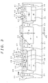
- FIG. 1 shows a schematic cross sectional view of the semiconductor device according to an embodiment of the present invention.
- the J-FET device is comprised of n-channel field-effect-transistors that are integrated with n-p-n transistors on a common substrate.
- the device is fabricated on a p-type single crystal silicon substrate 21.
- An n + -buried layer 22 is formed on the substrate 21, and an epitaxial layer 23 formed on top of the layers 21,22 is separated into a plurality of island regions 25 by the junctions of the p + -type separation regions 24.
- a p + buried region 26 is formed to superimpose on the n + buried layer 22 so that the p + buried layer 26 can be linked to a p-well region 27 formed by diffusion of dopant from the surface of the island region 25.
- n-type channel region 28 and a p + -type top gate region 29 are provided on the top surface of the p-well region 27 so as to bury the n-type channel region 28 (constituting the channel) below the surface of the epitaxial layer 23.
- the P-well region 27 operates as the back gate.
- P + -type gate-contact regions 30 are formed to superimpose on the ends of the channel region 28 and the top gate region 29 so as to overlap the low concentration diffusion regions of the well region 27.
- An n + type source region 31 and a drain region 32 are formed so as to penetrate through the channel region 28.
- the present transistor device controls the channel current between the source/drain regions by forming a depletion layer in the channel region 28 according to the magnitude of the voltage applied between the source electrode 33 and the drain electrode 34 through the gate electrode 35.
- a collector region (layer) 60 is formed by dopant diffusion to extend from the surface of the epitaxial layer 23 to the n + buried layer 22.
- a p-type base region 36 is formed on the surface of the collector region 60, and an n + emitter region 37 is formed on the surface of the base region 36 so that the collector region 60 completes the structure of an n-p-n transistor device having an emitter electrode 39, a base electrode 40 and a collector electrode 41 in contact with an n + collector contact region 38.
- Electrodes groups form an integrated circuit network by making ohmic contacts to the surface of each respective diffusion region, and extending over the silicon film 42 that covers the epitaxial layer 23 so as to provide various component connections.
- the gate electrode 35 connected to the gate of J-FET is extended over the oxide film 42, and continues to the expansion electrode 43 comprised by circular patterns of diameters ranging from 10 to 1.5 mm, for example.
- the expansion electrode 43 is connected to the electric condenser microphone.
- the bottom section of the expansion electrode 43 opposes an island region 25 with an intervening p + separation region 24 by way of the oxide film 42.
- the p + buried layer 22 is not provided. Also, circuit elements are not housed in any containers.
- the ground potential GND is applied to the substrate 21 through the electrode 45 by way of the junction separation region and the back electrode for separation of junctions.
- the bottom section of the island region 25 below the expansion electrode 43 is used in a floating condition without having any potential applied.
- Figure 4 shows a plan view of the overall semiconductor device.
- the size of the device chip 50 is about 2.5x3.0 mm, and the expansion electrode 43 having a diameter between 1.0 ⁇ 1.5 mm is disposed at about the center of the chip 50, and a part of the expansion electrode 43 is extended to contact the gate electrode 35 of the J-FET.
- a plurality of bonding pads 52 are provided about the periphery of the chip 50.
- the bonding pad has a square shape with a perimeter length of about 100 ⁇ 300 ⁇ m.
- Other elements of the device for example, n-p-n transistor, resistance element and capacitive element are arranged in the free area so as to surround the expansion electrode 43.
- Figure 5 shows an equivalent circuit. Because the epitaxial layer 23 is made as a high resistivity region, the series resistance of the island regions 25 is quite high. Also, the depletion layer which is expected to be formed between the substrate 21 and around the boundary sections, is quite expanded, resulting that the value of the parasitic capacitance C1 becomes quite low. If the depletion layer is expanded to a degree to fill the enitre area of the island regions 25, the value of capacitance C1 is minimized, and even if it does not expand to such an extent, the circuit connection can be almost severed because of the effect of increasing series resistance. Therefore, it is possible to prevent signal leakage from the expansion electrode 43 to the substrate 21.
- capacitance C3 is generated by the p-n junction between the island region 25 and the separation region 24, when they are considered in comparison of the areas involved, capacitance C3 represents quite a low value that can be ignored, for example, several nF compared with several tens of pF for C1. If it is necessary to consider the effects of capacitance C3, it is preferable to design a circuit so that there are no ground potential electrodes in the separation regions 24 surrounding the expansion electrode 43.
- the collector region 60 is formed so that the doping concentration and its concentration profile are such as to permit the collector region 60 to function as the collector for the n-p-n transistor.
- the device is fabricated with the island regions 25 having the J-FET device in the floating state, and furthermore, the high resistivity structure of the epitaxial layer 23 is left therein. Accordingly, by expanding the depletion regions, generated at the junctions between the p-type regions (such as p + buried layer 27, p-well region 26, gate contact region 30) impressed with the gate potential and the island regions 25, the parasitic capacitance values with reference to the ground potential GND are minimized. This effect contributes also to preventing the current leakage from the expansion electrode 43 to the ground potential.
- the p-type regions such as p + buried layer 27, p-well region 26, gate contact region 30
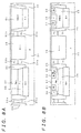
- Step 1 referring to Figure 6A
- a semiconductor substrate 21 is prepared. The surface is heated to produce an oxide film thereon, and openings in the oxide film are produced by photo-etching technology. Antimony (Sb) is diffused in the substrate so as to produce an n + buried layer 22. Then, oxide film is re-formed and openings are fabricated by photo-etching technology again, and boron (B) ions are injected to produce a p + buried layer 26 and separation regions 24a on the surface of the substrate 21.
- Sb Antimony
- B boron
- n-type epitaxial layer 23 is formed by vapor deposition. Film thickness of 5 ⁇ 12 ⁇ m is obtained and the resistivity ⁇ is adjusted to 100 ⁇ 5000 ⁇ cm. Such a high resistivity value can be obtained by carrying out the vapor deposition process without doping.
- Si oxide film is formed on the surface of the epitaxial layer 23, and a resist masking layer is formed on the oxide film.
- Boron (B, BF 2 ) ions are injected through the openings produced on the resist masking layer to produce p-type well regions 27. Further, the resist masking layer is replaced with another resist masking layer, and a collector region 60 is formed by P-ion implantation in the required regions for making n-p-n transistors.
- the entire substrate is subjected to heating at 1100 °C for 1 ⁇ 3 hours to produce thermal diffusion in the p-well regions 27 and the collector region 60 produced by P-ion implantation.
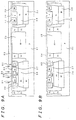
- SiO 2 film formed on the epitaxial layer 23 by the previouss heat treatment process After removing the SiO 2 film formed on the epitaxial layer 23 by the previouss heat treatment process, another SiO 2 film of about 500 ⁇ thickness is re-deposited.
- Photo-resist masking layer for ion-implantation is formed on the SiO 2 film, and openings are fabricated in the regions corresponding to the base regions 36 of the n-p-n transistors and gate contact regions 30. Boron-ion implantation is carried out to provide doping on the surface exposed through the openings.
- base diffusion is carried out at 1100 °C for 1-2 hours.
- Diffusion process is carried out so that the diffused layers of the base region 36 and the gate contact region 30 are shallower than the diffusion layer of the p-well regions 27, and that the gate contact region 30 extends over the top sections of the p-n junction sections formed by the p-well regions 27 and the n-type island regions 25.
- the gate contact region 30 surrounds the periphery of p-well region 27 in a ring shape.
- resist masking layer is re-applied so that a masking layer 63 is formed on the Silicon oxide layer for making openings 62 in those regions corresponding to channel regions 28.
- the edge of the opening 62 is located above the gate contact region 30 to expose the surface of the well region 27 and inner periphery of the ring-shaped gate contact region 30.
- the channel regions 28 are formed by ion-implantation of a p-type dopant, As or P, at a concentration in a range of 10 12 ⁇ 10 13 atoms/cm 3 .
- the masking layer is removed, and the emitter diffusion process is carried out at 1000 °C for 30 ⁇ 60 minutes to thermally diffuse emitter regions 37, source regions 31, and drain regions 32, and at the same time, to carry out thermal diffusion for the channel regions 28 and the top gate regions 29.
- ion-implantation and heat treating processes for the channel regions 28 and the top gate regions 29 may be carried out after completing the emitter diffusion process.
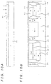
- contact holes 65 are produced on the silicon oxide film 64 thermally-formed on the expitaxial layer 23 using a normal photo-etching technology. Those regions where expansion electrode 43 is formed, are already provided with silicon oxide film 64 of 8000 ⁇ 20,000 ⁇ thickness, but the thickness of the oxide film may be increased further by depositing silicon oxide or silicon nitride film using CVD(chemical vapor deposition).
- the entire surface of the substrate is coated with aluminum film of a thickness in a range of 1.0 ⁇ 3.0 ⁇ m, by using sputtering or vacuum vapor deposition method and photo-etched using normal photo-etching method, to provide source electrodes 33, drain electrodes 34, gate electrodes 35, emitter electrodes 39, base electrodes 40, collector electrodes 41, ground electrodes 45 and expansion electrodes 43 to produce the device shown in Figure 3.
- Figure 10 shows a cross sectional structure to illustrate a second embodiment to fabricating the device.
- collector region 60 was diffused from the surface of the epitaxial layer 23, but in this method, diffusion is carried out from the surfaces of both the surfaces of the substrate 21 and the epitaxial layer 23.
- a p-type substrate 21 is prepared, and a selective photo-resist masking layer is formed on the surface of the substrate 21 so that the buried collector layer 61 can be produced by carrying out ion-implantation of n-type dopant, As or Sb and others, for those regions intended for making n-p-n transistors, and heat treating to thermally diffuse the dopants.
- n-type dopant As or Sb and others
- the junction structure of the collector layer is produced by joining the collector region 60 and the buried collector layer 61 to obtain the structure shown in Figure 10B. Subsequent steps are the same as those shown in Figures 8B ⁇ 9B. Heat treating process is shortened because the diffusion process can be carried out from the top surface as well as from the bottom surface of the epitaxial layer.
- the structure of the J-FET was formed using n-type channels, but p-type channel J-FET can also be produced.
- input transistor was represented by J-FET, but n- or p-channel type MOSFET can also be used to produce the present semiconductor device.
Landscapes
- Junction Field-Effect Transistors (AREA)
- Bipolar Transistors (AREA)
- Bipolar Integrated Circuits (AREA)
- Metal-Oxide And Bipolar Metal-Oxide Semiconductor Integrated Circuits (AREA)
- Circuit For Audible Band Transducer (AREA)
- Pressure Sensors (AREA)
- Element Separation (AREA)
- Thin Film Transistor (AREA)
Applications Claiming Priority (2)
| Application Number | Priority Date | Filing Date | Title |
|---|---|---|---|
| JP06141599A JP3634660B2 (ja) | 1999-03-09 | 1999-03-09 | 半導体装置 |
| JP6141599 | 1999-03-09 |
Publications (2)
| Publication Number | Publication Date |
|---|---|
| EP1035575A2 true EP1035575A2 (fr) | 2000-09-13 |
| EP1035575A3 EP1035575A3 (fr) | 2001-10-17 |
Family
ID=13170468
Family Applications (1)
| Application Number | Title | Priority Date | Filing Date |
|---|---|---|---|
| EP00200833A Withdrawn EP1035575A3 (fr) | 1999-03-09 | 2000-03-08 | Dispositif semi-conducteur |
Country Status (4)
| Country | Link |
|---|---|
| US (2) | US6555857B1 (fr) |
| EP (1) | EP1035575A3 (fr) |
| JP (1) | JP3634660B2 (fr) |
| KR (1) | KR100366896B1 (fr) |
Cited By (1)
| Publication number | Priority date | Publication date | Assignee | Title |
|---|---|---|---|---|
| WO2006040735A1 (fr) * | 2004-10-14 | 2006-04-20 | Koninklijke Philips Electronics N.V. | Dispositif jfet compatible bicmos et procede de fabrication de ce dispositif |
Families Citing this family (7)
| Publication number | Priority date | Publication date | Assignee | Title |
|---|---|---|---|---|
| JP3634660B2 (ja) * | 1999-03-09 | 2005-03-30 | 三洋電機株式会社 | 半導体装置 |
| JP2006202987A (ja) * | 2005-01-20 | 2006-08-03 | Matsushita Electric Ind Co Ltd | 半導体装置およびその製造方法 |
| KR101045741B1 (ko) * | 2008-03-28 | 2011-06-30 | 산요 세미컨덕터 컴퍼니 리미티드 | 증폭 소자 및 그 제조 방법 |
| JP2009239202A (ja) * | 2008-03-28 | 2009-10-15 | Sanyo Electric Co Ltd | 増幅素子およびその製造方法 |
| CN102244077A (zh) * | 2011-05-30 | 2011-11-16 | 上海宝逊电声器材有限公司 | 一种驻极体麦克风内置电容专用管芯及其制备方法 |
| US9178058B2 (en) | 2013-03-13 | 2015-11-03 | Taiwan Semiconductor Manufacturing Company, Ltd. | RF switch on high resistive substrate |
| CN115274912B (zh) * | 2022-08-01 | 2024-01-30 | 中国电子科技集团公司第四十四研究所 | 高空间分辨率的x射线探测器单元、探测器及其制作方法 |
Family Cites Families (11)
| Publication number | Priority date | Publication date | Assignee | Title |
|---|---|---|---|---|
| JPS58197885A (ja) | 1982-05-14 | 1983-11-17 | Nec Corp | 半導体装置 |
| JPS61160963A (ja) | 1985-01-08 | 1986-07-21 | Sanyo Electric Co Ltd | コンデンサマイク用半導体装置 |
| JPS61242059A (ja) | 1985-04-19 | 1986-10-28 | Sanyo Electric Co Ltd | コンデンサマイク用半導体装置 |
| JPS62229869A (ja) * | 1985-12-03 | 1987-10-08 | Nec Corp | 半導体装置およびその製造方法 |
| GB2243485A (en) | 1990-04-27 | 1991-10-30 | Motorola Gmbh | Semiconductor device contact pads |
| JPH04291952A (ja) * | 1991-03-20 | 1992-10-16 | Sony Corp | 半導体装置 |
| JPH0547913A (ja) | 1991-08-12 | 1993-02-26 | Sharp Corp | 半導体装置の製造方法 |
| JP3217560B2 (ja) | 1993-11-15 | 2001-10-09 | 株式会社東芝 | 半導体装置 |
| DE69415500T2 (de) * | 1994-03-31 | 1999-05-20 | Stmicroelectronics S.R.L., Agrate Brianza, Mailand/Milano | Verfahren zur Herstellung eines Halbleiterbauteils mit vergrabenem Übergang |
| KR0182030B1 (ko) * | 1995-11-30 | 1999-03-20 | 김광호 | 바이시모스 트랜지스터 및 그 제조 방법 |
| JP3634660B2 (ja) * | 1999-03-09 | 2005-03-30 | 三洋電機株式会社 | 半導体装置 |
-
1999
- 1999-03-09 JP JP06141599A patent/JP3634660B2/ja not_active Expired - Fee Related
-
2000
- 2000-03-08 EP EP00200833A patent/EP1035575A3/fr not_active Withdrawn
- 2000-03-08 KR KR10-2000-0011437A patent/KR100366896B1/ko not_active Expired - Fee Related
- 2000-03-08 US US09/520,950 patent/US6555857B1/en not_active Expired - Lifetime
-
2002
- 2002-12-17 US US10/320,576 patent/US6960797B2/en not_active Expired - Fee Related
Cited By (2)
| Publication number | Priority date | Publication date | Assignee | Title |
|---|---|---|---|---|
| WO2006040735A1 (fr) * | 2004-10-14 | 2006-04-20 | Koninklijke Philips Electronics N.V. | Dispositif jfet compatible bicmos et procede de fabrication de ce dispositif |
| CN100521159C (zh) * | 2004-10-14 | 2009-07-29 | Nxp股份有限公司 | 与BiCMOS兼容的JFET器件及其制造方法 |
Also Published As
| Publication number | Publication date |
|---|---|
| US6555857B1 (en) | 2003-04-29 |
| KR100366896B1 (ko) | 2003-01-09 |
| US6960797B2 (en) | 2005-11-01 |
| JP3634660B2 (ja) | 2005-03-30 |
| US20030122167A1 (en) | 2003-07-03 |
| JP2000260786A (ja) | 2000-09-22 |
| KR20000076787A (ko) | 2000-12-26 |
| EP1035575A3 (fr) | 2001-10-17 |
Similar Documents
| Publication | Publication Date | Title |
|---|---|---|
| KR100564890B1 (ko) | 바이폴라/cmos집적회로의제조 | |
| US6770952B2 (en) | Integrated process for high voltage and high performance silicon-on-insulator bipolar devices | |
| US5610422A (en) | Semiconductor device having a buried insulated gate | |
| JPH04226066A (ja) | Bicmos装置及びその製造方法 | |
| US5990535A (en) | Power integrated circuit | |
| US5557131A (en) | Elevated emitter for double poly BICMOS devices | |
| JPH04226064A (ja) | 半導体装置用の相互接続体及びその製造方法 | |
| US6555857B1 (en) | Semiconductor device | |
| JP2587444B2 (ja) | Cmos技術を用いたバイポーラ・トランジスタとその製造方法 | |
| JP3530414B2 (ja) | 半導体装置 | |
| JPH04363046A (ja) | 半導体装置の製造方法 | |
| KR100305594B1 (ko) | 스마트전력집적회로의제조방법 | |
| JP3454734B2 (ja) | 半導体集積回路の製造方法 | |
| JP3762556B2 (ja) | 半導体集積回路装置およびその製造方法 | |
| JPH04226061A (ja) | バイポーラ・トランジスタとjfetトランジスタを形成する工程 | |
| JP2000150527A (ja) | ベ―スバラスト抵抗を使用するlpnp | |
| JP3634659B2 (ja) | 半導体装置 | |
| JP3439149B2 (ja) | 半導体装置 | |
| JP2006165370A (ja) | 半導体装置及びその製造方法 | |
| JP2000286194A (ja) | 半導体装置 | |
| KR20000028965A (ko) | 반도체 장치 및 그 제조 방법 | |
| JP3992645B2 (ja) | 半導体集積回路 | |
| JP3216307B2 (ja) | 半導体装置 | |
| JPH0553300B2 (fr) | ||
| KR20010057342A (ko) | 반도체장치의 제조방법 |
Legal Events
| Date | Code | Title | Description |
|---|---|---|---|
| PUAI | Public reference made under article 153(3) epc to a published international application that has entered the european phase |
Free format text: ORIGINAL CODE: 0009012 |
|
| AK | Designated contracting states |
Kind code of ref document: A2 Designated state(s): DE FR GB Kind code of ref document: A2 Designated state(s): AT BE CH CY DE DK ES FI FR GB GR IE IT LI LU MC NL PT SE |
|
| AX | Request for extension of the european patent |
Free format text: AL;LT;LV;MK;RO;SI |
|
| PUAL | Search report despatched |
Free format text: ORIGINAL CODE: 0009013 |
|
| AK | Designated contracting states |
Kind code of ref document: A3 Designated state(s): AT BE CH CY DE DK ES FI FR GB GR IE IT LI LU MC NL PT SE |
|
| AX | Request for extension of the european patent |
Free format text: AL;LT;LV;MK;RO;SI |
|
| RIC1 | Information provided on ipc code assigned before grant |
Free format text: 7H 01L 21/762 A, 7H 01L 23/522 B, 7H 01L 21/8249 B, 7H 01L 27/06 B, 7H 01L 29/808 B, 7H 01L 23/485 B, 7H 01L 21/761 B |
|
| 17P | Request for examination filed |
Effective date: 20020129 |
|
| AKX | Designation fees paid |
Free format text: DE FR GB |
|
| 17Q | First examination report despatched |
Effective date: 20070928 |
|
| GRAP | Despatch of communication of intention to grant a patent |
Free format text: ORIGINAL CODE: EPIDOSNIGR1 |
|
| STAA | Information on the status of an ep patent application or granted ep patent |
Free format text: STATUS: THE APPLICATION IS DEEMED TO BE WITHDRAWN |
|
| 18D | Application deemed to be withdrawn |
Effective date: 20100106 |