EP1067210A2 - Verfahren zur Abscheidung eines harten Kohlenstoff-Filmes auf einem Substrat und Klinge für einen elektrischen Rasierer - Google Patents
Verfahren zur Abscheidung eines harten Kohlenstoff-Filmes auf einem Substrat und Klinge für einen elektrischen Rasierer Download PDFInfo
- Publication number
- EP1067210A2 EP1067210A2 EP00120743A EP00120743A EP1067210A2 EP 1067210 A2 EP1067210 A2 EP 1067210A2 EP 00120743 A EP00120743 A EP 00120743A EP 00120743 A EP00120743 A EP 00120743A EP 1067210 A2 EP1067210 A2 EP 1067210A2
- Authority
- EP
- European Patent Office
- Prior art keywords
- substrate
- interlayer
- carbon film
- hard carbon
- plating
- Prior art date
- Legal status (The legal status is an assumption and is not a legal conclusion. Google has not performed a legal analysis and makes no representation as to the accuracy of the status listed.)
- Withdrawn
Links
Images


Classifications
-
- B—PERFORMING OPERATIONS; TRANSPORTING
- B26—HAND CUTTING TOOLS; CUTTING; SEVERING
- B26B—HAND-HELD CUTTING TOOLS NOT OTHERWISE PROVIDED FOR
- B26B19/00—Clippers or shavers operating with a plurality of cutting edges, e.g. hair clippers, dry shavers
- B26B19/38—Details of, or accessories for, hair clippers, or dry shavers, e.g. housings, casings, grips, guards
- B26B19/3846—Blades; Cutters
-
- B—PERFORMING OPERATIONS; TRANSPORTING
- B26—HAND CUTTING TOOLS; CUTTING; SEVERING
- B26B—HAND-HELD CUTTING TOOLS NOT OTHERWISE PROVIDED FOR
- B26B19/00—Clippers or shavers operating with a plurality of cutting edges, e.g. hair clippers, dry shavers
- B26B19/38—Details of, or accessories for, hair clippers, or dry shavers, e.g. housings, casings, grips, guards
- B26B19/3853—Housing or handle
-
- B—PERFORMING OPERATIONS; TRANSPORTING
- B26—HAND CUTTING TOOLS; CUTTING; SEVERING
- B26B—HAND-HELD CUTTING TOOLS NOT OTHERWISE PROVIDED FOR
- B26B21/00—Razors of the open or knife type; Safety razors or other shaving implements of the planing type; Hair-trimming devices involving a razor-blade; Equipment therefor
- B26B21/54—Razor-blades
- B26B21/58—Razor-blades characterised by the material
- B26B21/60—Razor-blades characterised by the material by the coating material
-
- C—CHEMISTRY; METALLURGY
- C23—COATING METALLIC MATERIAL; COATING MATERIAL WITH METALLIC MATERIAL; CHEMICAL SURFACE TREATMENT; DIFFUSION TREATMENT OF METALLIC MATERIAL; COATING BY VACUUM EVAPORATION, BY SPUTTERING, BY ION IMPLANTATION OR BY CHEMICAL VAPOUR DEPOSITION, IN GENERAL; INHIBITING CORROSION OF METALLIC MATERIAL OR INCRUSTATION IN GENERAL
- C23C—COATING METALLIC MATERIAL; COATING MATERIAL WITH METALLIC MATERIAL; SURFACE TREATMENT OF METALLIC MATERIAL BY DIFFUSION INTO THE SURFACE, BY CHEMICAL CONVERSION OR SUBSTITUTION; COATING BY VACUUM EVAPORATION, BY SPUTTERING, BY ION IMPLANTATION OR BY CHEMICAL VAPOUR DEPOSITION, IN GENERAL
- C23C16/00—Chemical coating by decomposition of gaseous compounds, without leaving reaction products of surface material in the coating, i.e. chemical vapour deposition [CVD] processes
- C23C16/02—Pretreatment of the material to be coated
- C23C16/0272—Deposition of sub-layers, e.g. to promote the adhesion of the main coating
-
- C—CHEMISTRY; METALLURGY
- C23—COATING METALLIC MATERIAL; COATING MATERIAL WITH METALLIC MATERIAL; CHEMICAL SURFACE TREATMENT; DIFFUSION TREATMENT OF METALLIC MATERIAL; COATING BY VACUUM EVAPORATION, BY SPUTTERING, BY ION IMPLANTATION OR BY CHEMICAL VAPOUR DEPOSITION, IN GENERAL; INHIBITING CORROSION OF METALLIC MATERIAL OR INCRUSTATION IN GENERAL
- C23C—COATING METALLIC MATERIAL; COATING MATERIAL WITH METALLIC MATERIAL; SURFACE TREATMENT OF METALLIC MATERIAL BY DIFFUSION INTO THE SURFACE, BY CHEMICAL CONVERSION OR SUBSTITUTION; COATING BY VACUUM EVAPORATION, BY SPUTTERING, BY ION IMPLANTATION OR BY CHEMICAL VAPOUR DEPOSITION, IN GENERAL
- C23C16/00—Chemical coating by decomposition of gaseous compounds, without leaving reaction products of surface material in the coating, i.e. chemical vapour deposition [CVD] processes
- C23C16/22—Chemical coating by decomposition of gaseous compounds, without leaving reaction products of surface material in the coating, i.e. chemical vapour deposition [CVD] processes characterised by the deposition of inorganic material, other than metallic material
- C23C16/26—Deposition of carbon only
-
- C—CHEMISTRY; METALLURGY
- C23—COATING METALLIC MATERIAL; COATING MATERIAL WITH METALLIC MATERIAL; CHEMICAL SURFACE TREATMENT; DIFFUSION TREATMENT OF METALLIC MATERIAL; COATING BY VACUUM EVAPORATION, BY SPUTTERING, BY ION IMPLANTATION OR BY CHEMICAL VAPOUR DEPOSITION, IN GENERAL; INHIBITING CORROSION OF METALLIC MATERIAL OR INCRUSTATION IN GENERAL
- C23C—COATING METALLIC MATERIAL; COATING MATERIAL WITH METALLIC MATERIAL; SURFACE TREATMENT OF METALLIC MATERIAL BY DIFFUSION INTO THE SURFACE, BY CHEMICAL CONVERSION OR SUBSTITUTION; COATING BY VACUUM EVAPORATION, BY SPUTTERING, BY ION IMPLANTATION OR BY CHEMICAL VAPOUR DEPOSITION, IN GENERAL
- C23C28/00—Coating for obtaining at least two superposed coatings either by methods not provided for in a single one of groups C23C2/00 - C23C26/00 or by combinations of methods provided for in subclasses C23C and C25C or C25D
- C23C28/30—Coatings combining at least one metallic layer and at least one inorganic non-metallic layer
- C23C28/32—Coatings combining at least one metallic layer and at least one inorganic non-metallic layer including at least one pure metallic layer
- C23C28/321—Coatings combining at least one metallic layer and at least one inorganic non-metallic layer including at least one pure metallic layer with at least one metal alloy layer
-
- C—CHEMISTRY; METALLURGY
- C23—COATING METALLIC MATERIAL; COATING MATERIAL WITH METALLIC MATERIAL; CHEMICAL SURFACE TREATMENT; DIFFUSION TREATMENT OF METALLIC MATERIAL; COATING BY VACUUM EVAPORATION, BY SPUTTERING, BY ION IMPLANTATION OR BY CHEMICAL VAPOUR DEPOSITION, IN GENERAL; INHIBITING CORROSION OF METALLIC MATERIAL OR INCRUSTATION IN GENERAL
- C23C—COATING METALLIC MATERIAL; COATING MATERIAL WITH METALLIC MATERIAL; SURFACE TREATMENT OF METALLIC MATERIAL BY DIFFUSION INTO THE SURFACE, BY CHEMICAL CONVERSION OR SUBSTITUTION; COATING BY VACUUM EVAPORATION, BY SPUTTERING, BY ION IMPLANTATION OR BY CHEMICAL VAPOUR DEPOSITION, IN GENERAL
- C23C28/00—Coating for obtaining at least two superposed coatings either by methods not provided for in a single one of groups C23C2/00 - C23C26/00 or by combinations of methods provided for in subclasses C23C and C25C or C25D
- C23C28/30—Coatings combining at least one metallic layer and at least one inorganic non-metallic layer
- C23C28/34—Coatings combining at least one metallic layer and at least one inorganic non-metallic layer including at least one inorganic non-metallic material layer, e.g. metal carbide, nitride, boride, silicide layer and their mixtures, enamels, phosphates and sulphates
- C23C28/343—Coatings combining at least one metallic layer and at least one inorganic non-metallic layer including at least one inorganic non-metallic material layer, e.g. metal carbide, nitride, boride, silicide layer and their mixtures, enamels, phosphates and sulphates with at least one DLC or an amorphous carbon based layer, the layer being doped or not
-
- Y—GENERAL TAGGING OF NEW TECHNOLOGICAL DEVELOPMENTS; GENERAL TAGGING OF CROSS-SECTIONAL TECHNOLOGIES SPANNING OVER SEVERAL SECTIONS OF THE IPC; TECHNICAL SUBJECTS COVERED BY FORMER USPC CROSS-REFERENCE ART COLLECTIONS [XRACs] AND DIGESTS
- Y10—TECHNICAL SUBJECTS COVERED BY FORMER USPC
- Y10T—TECHNICAL SUBJECTS COVERED BY FORMER US CLASSIFICATION
- Y10T428/00—Stock material or miscellaneous articles
- Y10T428/30—Self-sustaining carbon mass or layer with impregnant or other layer
-
- Y—GENERAL TAGGING OF NEW TECHNOLOGICAL DEVELOPMENTS; GENERAL TAGGING OF CROSS-SECTIONAL TECHNOLOGIES SPANNING OVER SEVERAL SECTIONS OF THE IPC; TECHNICAL SUBJECTS COVERED BY FORMER USPC CROSS-REFERENCE ART COLLECTIONS [XRACs] AND DIGESTS
- Y10—TECHNICAL SUBJECTS COVERED BY FORMER USPC
- Y10T—TECHNICAL SUBJECTS COVERED BY FORMER US CLASSIFICATION
- Y10T428/00—Stock material or miscellaneous articles
- Y10T428/31504—Composite [nonstructural laminate]
- Y10T428/31678—Of metal
Definitions
- the present invention relates to a method for providing a hard carbon film on a substrate, more particularly to a method for providing a protective film such as on inner and outer blades of an electric shaver, magneto-optical disks, thin film magnetic heads and surface acoustic wave (SAW) devices; an antireflection film for lithography; a protective film on sliding surfaces of compressors; or a hard carbon film such as on constituent layers of solar batteries, decorative articles and optical parts.
- a protective film such as on inner and outer blades of an electric shaver, magneto-optical disks, thin film magnetic heads and surface acoustic wave (SAW) devices
- SAW surface acoustic wave
- Japanese Patent Laying-Open Nos. 7-41386(1995) and 7-316818(1995) disclose that the adhesion between a hard carbon film and a substrate can be improved by providing an interlayer of Si, Ru or Ge therebetween even when the substrate is made of a metal or an alloy principally formed of Ni or Al, suitably used such as for an electric shaver blade, or of a stainless steel.
- the above-described prior art interlayer is effective in improving adhesion and peel resistance between the substrate and the hard carbon film, e.g. the diamond-like carbon film if interposed therebetween.
- the other type of interlayer which is also capable of improving the adhesion and peel resistance between the substrate and the hard carbon film.
- the above-described conventional interlayers have been formed by vapor phase epitaxial methods such as a sputtering method and a plasma CVD method. This requires that the thickness of the interlayer be made greater, or alternatively, the substrate position be changed during the interlayer formation if the substrate has a complicated three-dimensional configuration.
- the hard carbon film-coated substrate in accordance with a first aspect of the present invention includes a substrate, a hard carbon film and an interlayer formed between the substrate and the hard carbon film.
- the interlayer is principally comprised of at least one selected from the group consisting of Al, Cr, Sn, Co and B, oxides, nitrides and carbides thereof.
- any method such as sputtering can be employed to form the interlayer in accordance with the first aspect of the present invention.
- the sputtering method it is preferred to form the interlayer while applying a radio frequency voltage to a substrate so that a self-bias voltage is produced across the substrate.
- the self-bias voltage produced in the substrate is controlled not to exceed -20 V to assure the enhanced adhesion of the hard carbon film to the substrate.
- the interlayer in accordance with the first aspect of the present invention may be formed using other physical deposition or chemical vapor phase epitaxial methods.
- Plating may be employed to form a metallic interlayer, for example.
- hard carbon film as used in the first aspect of the present invention is intended to include an amorphous diamond-like carbon film, a diamond-like carbon film having amorphous and crystalline portions, and a crystalline diamond-like carbon film.
- a method of forming the hard carbon film in the first aspect of the present invention is not particularly limited.
- the hard carbon film can be formed such as by a CVD method, e.g. a plasma CVD method.
- a CVD method e.g. a plasma CVD method.
- the self-bias voltage produced in the substrate is controlled not to exceed -20 V.
- an electron cyclotron resonance (ECR) plasma CVD apparatus can be employed as a means for generating a plasma, for example. The use of such an apparatus increases a plasma density and enables a high-quality hard carbon film to be formed at low temperatures.
- ECR electron cyclotron resonance
- the hard carbon film-coated film in accordance with the first aspect of the present invention is applicable to inner and outer blades of an electric shaver, for example.
- Those inner and outer electric shaver blades are typically formed of a metal or an alloy principally comprised of Ni or Al, or of a stainless steel. Accordingly, a substrate formed of these materials can be employed as a substrate in the first aspect of the present invention.
- the substrate is not limited to the inner and outer blades of an electric shaver, but is also applicable to magneto-optical disks, thin film magnetic heads and surface acoustic wave (SAW) devices.
- the hard carbon film may be provided thereon to serve as a protective film therefor. Also, the hard carbon film may be provided to serve as an antireflection film which can be used during exposure in a lithography method. Furthermore, the hard carbon film may be provided to serve as a protective film for sliding parts of a compressor such as a rotary compressor, as a solar cell protective film layer, as an optical part, or as a part of decorative articles.
- the material types of the substrate in accordance with the first aspect of the present invention include cast irons such as Mo-Ni-Cr cast irons, steel such as high-speed tool steel, stainless steel such as SUS 304, ferrous alloys, non-ferrous metallic materials, ceramics, noble metals, and carbons.
- the non-ferrous metallic materials and ceramics include a single, alloy or sintered form of Ti, Al, Zr, Si, W, Mo, In, Ta, Fe, Ni, Co, Mn, Cr or Zn; and oxides, nitrides and carbides thereof.
- the noble metals include Au, Ag, Pt, Ru and Pd.
- the carbons include aluminum-impregnated carbons.
- a method for providing a hard carbon film on a substrate includes the steps of forming an interlayer on the substrate by plating and forming the hard carbon film on the interlayer.
- a method includes the steps of deposition-forming a substrate on a mold through electroforming, forming an interlayer on the substrate by plating, and forming a hard carbon film on the interlayer.
- the interlayer can be formed while the substrate is held on the mold. This eliminates the necessity of disengaging the substrate from the mold to thereby increase the productivity of the resulting hard carbon film-coated articles.
- the hard carbon film in accordance with the second aspect of the present invention includes an amorphous diamond-like carbon film and a diamond-like carbon film containing crystallites. It further includes a crystalline diamond-like carbon film.
- a method of forming the hard carbon film is not particularly limited.
- the hard carbon film can be formed such as by a CVD method.
- a plasma CVD method can be employed, for example, to form the hard carbon film while applying a radio frequency voltage to a substrate so that a self-bias voltage is produced across the substrate. In such an event, it is preferred that the self-bias voltage produced in the substrate is controlled not to exceed -20 V.
- an electron cyclotron resonance (ECR) plasma CVD apparatus can be employed as a means for generating a plasma, for example. The use of such an apparatus increases a plasma density and enables a high-quality hard carbon film to be formed at low temperatures.
- plating techniques may be adopted which include electroplating and electroless plating.
- electroplating it is generally required that at least a surface of the substrate be electrically conductive.
- the interlayer is formed by plating. This enables the interlayer to be formed to a uniform thickness even on the substrate having complicated three-dimensional configurations. Accordingly, the interlayer can be uniformly formed even on substrate edge portions which have been difficult to be covered through thin film formation by conventional vapor phase methods. As a consequence, the adhesion of the hard carbon film to the substrate is enhanced. Also, such a uniform formation of the interlayer permits an average thickness of the interlayer to be controlled smaller than that of the interlayer formed by conventional vapor phase methods.
- the thickness of the interlayer in accordance with the second aspect of the invention is not particularly specified, but is preferably in the range of 50-5000 ⁇ , more preferably in the range of 100-3000 ⁇ .
- the interlayer can be uniformly formed even on a substrate having the above-described complicated three-dimensional configurations. Accordingly, the present method is advantageously applicable to a substrate having complicated three-dimensional configurations, e.g. inner and outer blades of an electric shaver.
- the electric shaver blades are generally formed of a metal or an alloy principally comprised of Ni or Al, or stainless steel.
- the second aspect of the present invention is advantageously applicable to those substrates.
- the substrate is not limited to the inner and outer blades of an electric shaver, but is also applicable to magneto-optical disks, thin film magnetic heads and surface acoustic wave (SAW) devices.
- the hard carbon film may be provided thereon to serve as a protective film therefor. Also, the hard carbon film may be provided to serve as an antireflection film which can be used during exposure in a lithography method. Furthermore, the hard carbon film may be provided to serve as a protective film for sliding parts of a compressor such as a rotary compressor, as a solar cell protective film layer, as an optical part, or as a part of decorative articles.
- the material types of the substrate in accordance with the second aspect of the present invention include cast irons such as Mo-Ni-Cr cast irons, steel such as high-speed tool steel, stainless steel such as SUS 304, ferrous alloys, non-ferrous metallic materials, ceramics, noble metals, and carbons.
- the non-ferrous metallic materials and ceramics include a single, alloy or sintered form of Ti, Al, Zr, Si, W, Mo, In, Ta, Fe, Ni, Co, Mn, Cr or Zn; and oxides, nitrides and carbides thereof.
- the noble metals include Au, Ag, Pt, Ru and Pd.
- the carbons include aluminum-impregnated carbons.
- interlayer material which can be formed by plating and enhance the adhesion between the substrate and the hard carbon film may be utilized.
- the specific examples of the interlayer materials include metals such as Ru, Cr, Sn and Co, and alloys principally comprised thereof.
- the interlayer in the second aspect of the present invention may be formed by composite plating which disperses fine particles such as of ceramics throughout a resulting metallic film.
- composite plating can be accomplished by conventionally known techniques.
- the metallic film containing fine particles in a dispersed form can be generally produced by plating in a plating bath containing dispersions of fine particles.
- Examples of the fine particles dispersed in the composite metallic film include oxides, nitrides and carbides of Al, Ru, Ti, Cr, Sn, Co, Si, B or Zr.
- the content of fine particles dispersed in the metallic film is preferably in the range of 0.1-30 volume %, more preferably in the range of 1-10 volume %.
- the preferred particle size of the fine particles is not greater than 1 ⁇ m.
- the fine particles dispersed in the metallic film are effective in enhancing the adhesion to the overlying hard carbon film.
- the material which constitutes a matrix in the metallic film can be selected from a wider range of materials than the above-described materials for the metallic film.
- the adhesion of the hard carbon film to a Ni substrate can be improved by plating on the Ni substrate the material identical to that of the substrate, i.e. Ni, to form a Ni film in which the fine particles are dispersed.
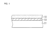
- Figure 1 is a cross-sectional view of one embodiment of a hard carbon film-coated substrate in accordance with a first aspect of the present invention.
- a hard carbon film i.e. a diamond-like carbon film 33 is formed.
- the thickness of the interlayer 32 is preferably in the range of 50-8000 ⁇ , more preferably in the range of 50-4000 ⁇ .
- the thickness of the diamond-like carbon film 33 is preferably in the range of 50-5000 ⁇ , more preferably in the range of 50-3000 ⁇ .
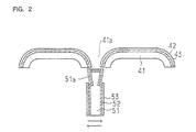
- Figure 2 is a cross-sectional view of an electric shaver blade embodiment in which the present invention is applied to its inner and outer blades.
- an outer blade substrate 41 formed on an outer blade substrate 41 is an interlayer 42 on which a hard carbon film, i.e. a diamond-like carbon film 43 is formed.
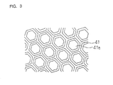
- Figure 3 is a plan view showing a planar pattern of the outer blade substrate 41. As illustrated in Figure 3, the outer blade substrate 41 has a number of holes 41a for catching beards.
- an inner blade is arranged inwardly of the outer blade substrate 41.
- an interlayer 52 on which a hard carbon film, i.e. a diamond-like carbon film 53 is formed.
- Figure 4 is a front view of the inner blade substrate 51.
- the inner blade substrate 51 has at its upper end tapered surfaces 51a each of which shows a downward slope (also refer to Figure 2) from an upper edge when cross-sectioned.
- the beards caught in the holes 41a are cut.
- the outer blade substrate 41 is formed of Ni whereas the inner blade substrate 51 is formed of stainless steel (SUS).
- FIG. 5 is a schematic block diagram of a thin film formation apparatus within which both of the interlayer and the hard carbon film can be formed.
- a plasma generation chamber 4 disposed interior of a vacuum chamber 8 is a plasma generation chamber 4 to which one end of a waveguide 2 is connected.
- the waveguide 102 has another end to mount a microwave supplying means 1.
- the microwaves generated within the microwave supplying means 1 pass through the waveguide 2 and a microwave inlet window 3 to be guided into the plasma generation chamber 4.
- a discharge gas inlet line 5 for introducing a discharge gas such as argon (Ar) into the plasma generation chamber 4.
- a plurality of plasma magnetic field generators 6 are mounted circumferentially of the plasma generation chamber 4.
- a high-density plasma can be produced within the plasma generation chamber 4 by influencing a high-frequency magnetic field produced by the microwave upon the magnetic field produced by the plasma magnetic field generators 6.
- a drum-shaped substrate holder 12 is provided within the vacuum chamber 8 so as to be rotatable about an axis (not shown) which arranged perpendicularly to a wall surface of the vacuum chamber 8.
- a number of substrates 13 is arranged circumferentially of the substrate holder 12 at regular intervals.
- a high-frequency power source 10 is connected to the substrate holder 12.
- the shielding cover 14 is connected to a grounded electrode.
- the shielding cover 14 functions to prevent generation of discharges between the vacuum chamber 8 and the substrate holder 12 excluding target film-forming locations thereon, which discharges will be otherwise generated when a radio frequency (also referred to as RF) voltage is applied to the substrate holder 12 for film-forming.
- the spacing between the substrate holder 12 and the shielding cover 14 may be dimensioned to be smaller than a mean free path of gaseous molecules.
- the mean free path of gaseous molecules is equal to or smaller than the average distance that ions or electrons accelerated by an electric field can travel without collisions.
- the probability of collisions between the gaseous molecules and the ions or electrons can be lowered to thereby prevent the molecules from undergoing chain electrolytic dissociations by dimensioning the spacing between the substrate holder 12 and the shielding cover 14 not to exceed the mean free path of the gaseous molecules. It is preferred that the spacing between the substrate holder 12 and the shielding cover 14 is dimensioned not to exceed one tenth of the mean free path of the gaseous molecules. In this particular embodiment of the apparatus, the spacing between the substrate holder 12 and the shielding cover 14 is dimensioned to be about 5 mm so as not to exceed one tenth of the mean free path of the gaseous molecules.
- the shielding cover 14 has at its top a first opening 15. A plasma from the plasma generation chamber 4 is directed to pass through the first opening 15 to impact the substrates 13 mounted on the substrate holder 12.
- the vacuum chamber 8 is equipped with a reaction gas inlet line 16. A leading end of the reaction gas inlet line 16 is positioned above the first opening 15.
- Figure 6 is a plan view showing the leading end of the reaction gas inlet line 16 and its vicinities.
- the reaction gas inlet line 16 includes a gas inlet portion 16a for introducing a CH 4 gas into the vacuum chamber 8 and a gas discharge portion 16b for perpendicular connection to the gas inlet portion 16a.
- the gas discharge portion 16b is arranged to perpendicularly cross a rotational direction A of the substrate holder 12 and is positioned above the first opening 15.
- the gas discharge portion 16b is located upstream along the direction A within the first opening 15.
- the gas discharge portion 16b has a plurality of holes 21 which are directed downwardly each at an angle of about 45 degrees. In this particular embodiment, eight holes 21 are provided as shown in Figure 6.
- holes 21 are spaced from each other at distances which become smaller toward each end of the gas discharge portion 16b.
- the provision of the holes 117 at such spacings allows the CH 4 gas introduced from the gas inlet portion 16a to be discharged therefrom with a substantially uniform distribution along the length of the gas discharge portion 16b.
- the shield cover 14 has at its bottom a second opening 17 facing the first opening 15.
- a target 18 is disposed below the second opening 17 to upwardly face the second opening 17.
- an RF power source 19 for sputtering the target 18.
- the target 18 and the RF power source constitutes a means for forming the interlayer. Accordingly, in the apparatus of Figure 5, the hard carbon film is formed by the plasma CVD method at a location of the first opening 15 while the interlayer is formed by sputtering at a location of the second opening 17.
- the apparatus of Figure 5 was employed to form the interlayer and the diamond-like carbon film.
- a partial pressure of the Ar gas within the vacuum chamber 8 was set at 1.5 x 10 -3 Torr.
- B was used as the target 18 and a power supplied to the target 18 was set at 200 W.
- the interlayer comprised of B was formed on the Ni substrate 13 by applying a RF voltage to the substrate holder 12 such that a self-bias voltage produced in the substrate 13 reached -50 V. This step was continued for 30 minutes. As a result, the interlayer was formed to a thickness of about 0.05 ⁇ m.
- twenty four of the Ni substrates 13 were mounted circumferentially of the substrate holder 12 at regular intervals. In forming the interlayers on the respective substrates 13, the substrate holder 12 was rotated at a speed of about 10 rpm.
- a hard carbon film, i.e. a diamond-like carbon film was then formed on the interlayer overlying the Ni substrate 13.
- An interior of the vacuum chamber 8 was controlled at a pressure of 10 -5 -10 -7 Torr.
- the Ar gas at 5.7 x 10 -4 torr. was then supplied from the discharge gas inlet line 5 of the ECR plasma generator while a 2.45 GHz, 100 W microwave was supplied from the microwave supplying means 1, so that an Ar plasma generated within the plasma generation chamber 4 struck a surface of each substrate 13.
- a 13.56 MHz RF voltage from the high-frequency power source 10 was applied to the substrate holder 12 in a controlled fashion so that a self-bias voltage of -50 V was generated in each of the substrates 13.
- a CH 4 gas at 1.3 x 10 -3 Torr. was supplied through the reaction gas inlet line 16. This step was continued for about 15 minutes to form the diamond-like carbon film having a thickness of 1000 ⁇ on the surface of each substrate 13.
- the apparatus of Figure 5 was employed as similar to Example 1.
- the partial pressures of Ar and N 2 gases were set at 1.5 x 10 -3 Torr. and 5.0 x 10 -4 Torr., respectively.
- B was used as the target and a power supplied to the target was set at 200 W.
- the interlayer comprised of nitride of B was thus formed on the Ni substrate 13.
- a RF voltage was applied to the substrate holder 12 so that a self-bias voltage produced in the substrate 13 reached -50 V. This interlayer formation was continued for 40 minutes.
- the interlayer comprised of BN was formed to a thickness of about 0.05 ⁇ m.
- the diamond-like carbon film was formed on the interlayer to a thickness of 1000 ⁇ in the same manner as in Example 1.
- the apparatus of Figure 5 was employed as similar to Example 1.
- the partial pressures of Ar and O 2 gases were set at 1.5 x 10 -3 Torr. and 1.0 x 10 -3 Torr., respectively.
- Al was used as the target and a power supplied to the target was set at 400 W.
- the interlayer comprised of oxide of Al was thus formed on the Ni substrate 13.
- a RF voltage was applied to the substrate holder 12 so that a self-bias voltage of -50 V was produced in the substrate 13.
- This interlayer formation was continued for 30 minutes.
- the interlayer was formed to a thickness of about 0.04 ⁇ m.
- the diamond-like carbon film was formed on the interlayer to a thickness of 1000 ⁇ in the same manner as in Example 1.
- the apparatus of Figure 5 was employed as similar to Example 1.
- the partial pressures of Ar and N 2 gases were set at 1.5 x 10 -3 Torr. and 1.0 x 10 -3 Torr., respectively.
- Cr was used as the target and a power supplied to the target was set at 400 W to form the interlayer, comprised of nitride of Cr, on the Ni substrate 13.
- a RF voltage was applied to the substrate holder 12 so that a self-bias voltage of -50 V was produced in the substrate 13.
- This interlayer formation was continued for 30 minutes.
- the interlayer was formed to a thickness of about 0.05 ⁇ m.
- the diamond-like carbon film was formed on the interlayer to a thickness of 1000 ⁇ in the same manner as in Example 1.
- the apparatus of Figure 5 was employed as similar to Example 1.
- the partial pressures of Ar and O 2 gases were set at 1.5 x 10 -3 Torr. and 1.0 x 10 -3 Torr., respectively.
- Sn was used as the target and a power supplied to the target was set at 400 W to form the interlayer, comprised of oxide of Sn, on the Ni substrate 13.
- a RF voltage was applied to the substrate holder 12 so that a self-bias voltage of -50 V was produced in the substrate 13.
- This interlayer formation was continued for 30 minutes. As a result, the interlayer was formed to a thickness of about 0.04 ⁇ m.
- the diamond-like carbon film was formed on the interlayer to a thickness of 1000 ⁇ in the same manner as in Example 1.
- the apparatus of Figure 5 was employed as similar to Example 1.
- the partial pressure of Ar was set at 1.5 x 10 -3 Torr.
- Co was used as the target and a power supplied to the target was set at 400 W to form the interlayer, comprised of Co, on the Ni substrate 13.
- a RF voltage was applied to the substrate holder 12 so that a self-bias voltage of - 50 V was produced in the substrate 13.
- This interlayer formation was continued for 30 minutes.
- the interlayer was formed to a thickness of about 0.05 ⁇ m.
- the diamond-like carbon film was formed on the interlayer to a thickness of 1000 ⁇ in the same manner as in Example 1.
- a diamond-like carbon film was directly formed on a Ni substrate without intervention of an interlayer therebetween.
- the diamond-like carbon film formation was performed in the same conditions as used in Example 1.
- the diamond-like carbon film-coated Ni substrates as obtained in Examples 1-6 and Comparative Example 1 were evaluated for their levels of adhesion.
- each of the diamond-like carbon film-coated Ni substrates of Examples 1-6 which incorporated the interlayer in accordance with the first aspect of the invention, shows the number of its samples that experienced delamination as being much smaller relative the diamond-like carbon film-coated Ni substrate of Comparative Example 1. This demonstrates that the provision of the interlayer in accordance with the first aspect of the present invention enhances the adhesion of the diamond-like carbon film to the Ni substrate.
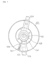
- Figure 7 is a schematic cross-sectional view showing a general construction of a rotary compressor.
- the rotary compressor includes a closed container 101, a crank shaft 102 driven by an electric motor (not shown), and a roller 103 mounted eccentric to the crank shaft 102.
- the roller 103 is made of Mo-Ni-Cr cast iron.
- a hollow cylinder 104 of cast iron is disposed to accommodate the roller 103 therein.
- the hollow cylinder 104 has a cylinder channel 105 within which a vane 106 reciprocates.
- the vane 106 partitions a space interior of the hollow cylinder 104 into a high-pressure part and a low-pressure part.
- the vane 106 is made of high-speed tool steel (SKH51).
- the vane 106 is urged against the roller 103 by a spring 107.
- An inlet tube 108 is provided to supply a refrigerant carrier into the interior of the hollow cylinder 104.
- the refrigerant carrier pressurized and heated within the hollow cylinder 104 is exhausted through an exhaust tube 109 to the exterior of the compressor.
- the roller 103 mounted eccentric to the crank shaft 102 moves circumferentially along an inner surface of the hollow cylinder 104 while rotating. Since the vane 106 is urged against the roller 103 by both a pressurized gas and the spring 107, the vane 106 is brought into a constant contact with a periphery of the roller 3. Accordingly, a rotational motion of the roller 103 is translated into a reciprocating motion of the vane 106 within the cylinder channel 105.
- the refrigerant carrier is suctioned through the inlet tube 108 into the interior of the hollow cylinder 104 within which the refrigerant carrier is compressed to increase its temperature and pressure before it is discharged through the exhaust tube 109 to the exterior of the rotary compressor.
- Figure 8 is a schematic cross-sectional view of the vane 106 carrying a hard carbon coating film thereon, in accordance with the first aspect of the present invention.
- Formed on the vane 106 is an interlayer 161 on which a hard carbon film 162 is formed.
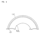
- Figure 9 is a schematic cross-sectional view of the roller 103 carrying thereon a hard carbon film, in accordance with the first aspect of the present invention.
- Formed on the roller 103 is an interlayer 131 on which a hard carbon film 132 is formed.
- Figure 10 is a schematic cross-sectional view of the cylinder channel 105 carrying thereon a hard carbon film, in accordance with the first aspect of the present invention.
- a hard carbon film 152 is formed on an inner surface of the cylinder channel 105 .
- the hard carbon film provided on the vane 106 of Figure 8 was then tested for evaluating its adhesion level.
- the apparatus of Figure 5 was employed.
- the partial pressure of Ar gas was set at 1.5 x 10 -3 Torr.
- Cr was used as a target and a power supplied to the target was set at 400 W to form a Cr interlayer on the vane 106.
- a RF voltage was applied to the substrate holder so that a self-bias voltage of -50 V was produced in the substrate.
- This interlayer formation was continued for 30 minutes. As a result, the interlayer was formed to a thickness of about 0.05 ⁇ m.
- Example 2 the hard carbon film formation was continued for 75 minutes in the same manner as in Example 1 so that the hard carbon film 162 was formed on the interlayer 161 to a thickness of about 5000 ⁇ .
- the hard carbon film-coated substrate thus obtained was tested for evaluating its level of adhesion.
- a hard carbon film was directly formed on the vane 106, without intervention of the Cr interlayer, by applying a RF voltage to the substrate holder such that a self-bias voltage of -50 V was produced in the vane 106.
- the obtained hard carbon film was also tested for evaluating its adhesion to the vane. Results are given in Table 2. Cr Interlayer Self-Bias Voltage (V) Number of Samples Absent -50 45 Present -50 5
- the interlayer was specified to be formed by sputtering.
- the method of forming the interlayer in accordance with the first aspect of the present invention is not limited to sputtering.
- the interlayer can be formed by the other methods including the other physical thin film formation methods such as deposition methods, chemical vapor phase epitaxial methods such as CVD methods, and plating methods.
- the apparatus of Figure 5 was employed in the above Examples to form both the interlayer and the hard carbon film, the other apparatuses may be employed to separately form the interlayer and the hard carbon film.
- the provision of the interlayer between the substrate and the hard carbon film in accordance with the first aspect of the present invention, enhances adhesion and peel resistance of the hard carbon film.
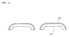
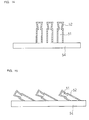
- Figure 11 is a cross-sectional view of an outer blade substrate 41 on which an interlayer 42 is formed by plating.
- the outer blade substrate may be electroformed, for example.
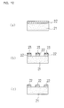
- Figure 12 are cross-sectional views showing the steps of forming the interlayer by plating, subsequent to electroforming the outer blade substrate.
- a metallic layer 22 is provided on a plastic plate 21 by plating nickel or applying a copper foil on the plastic plate 21.
- the metallic layer 23 is coated with a resist 23 in such a pattern as corresponding to an outer blade of an electric shaver.
- the resist 23 protects the coated area of the metallic layer 23 from the action of an etchant so that the metallic layer 23 is etched to the predetermined pattern of the outer blade for an electric shaver, as shown in Figure 12(b).
- the subsequent removal of the resist 23 leaves the metallic layer 22 having the pattern of the electric shaver outer blade on the plastic plate 21, as shown in Figure 12(c).
- a nickel plating is applied to the metallic layer 22 to obtain the outer blade substrate 41 for the electric shaver by electroforming.
- a commonly-employed electroplating bath may be utilized for the electroforming.
- An exemplary electroplating bath contains 30 g/l of nickel chloride, 300 g/l of nickel sulfamate, 30 g/l of boric acid, and a suitable amount of a pit inhibitor.
- the electroplating may be carried out in the pH range of 3.5-4.0, at temperatures of 30-60 °C and current densities of 2-15 A/dm 2 , for example, to deposit a nickel layer.
- the thickness of the nickel layer to be deposited is not particularly specified, but is generally in the range of 10-100 ⁇ m.
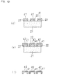
- the interlayer 42 is subsequently formed on the outer blade substrate 41 such as by electroplating or electroless plating while the outer blade substrate 41 is held on the metallic layer 22, as shown in Figure 13(e).
- the suitable plating bath and conditions may be selected depending upon the type of the interlayer 42 to be deposited by plating.
- the thickness of the interlayer 42 generally ranges from about 50 to 5000 ⁇ .
- the outer blade substrate 41 for an electric shaver is obtained which carries the interlayer 42 thereon, as shown in Figure 13(f).
- a diamond-like or hard carbon film is then formed on the interlayer to obtain an electric shaver outer blade having the interlayer through which the hard carbon film is provided on the outer blade substrate.
- the hard carbon film may be formed on the interlayer 42 after the outer blade substrate 41 carrying the interlayer 42 has been removed from the metallic layer 22.
- the hard carbon film may be formed on the interlayer 42 while the outer blade substrate 41 carrying the interlayer 42 is held on the metallic layer 22. This follows that the outer blade substrate 41 is removed from the metallic layer 22 subsequent to the hard carbon film formation.
- a Ni plating bath used in electroforming the Ni substrate contained 30 g/l of nickel chloride, 300 g/l of nickel sulfamate, 30 g/l of boric acid, and a suitable amount of a pit inhibitor.
- the Ni plating bath was adjusted to a pH of 3.5 and controlled at a temperature of 50 °C.
- the electroforming was then initiated at a current density of 10 A/dm 2 to deposit the Ni substrate on a mold.
- the thickness of the Ni substrate was about 50 ⁇ m.
- the Ru plating was carried out while the Ni substrate was held on the mold to form the Ru interlayer on the Ni substrate.
- An Ru plating bath as employed contained 3 g/l of ruthenium sulfate, 6 g/l of sulfuric acid and a suitable amount of additives. The Ru plating bath was adjusted to a pH of about 1.5 and controlled at a temperature of about 50 °C. The Ru electroplating was then performed at a current density of 2 A/dm 2 to deposit the Ru interlayer on the Ni substrate. The thickness of the Ru interlayer was about 100 ⁇ .
- a diamond-like carbon film was formed on the Ru interlayer using the ECR plasma CVD apparatus.
- the partial pressures of the Ar and CH 4 gases were set at 5.7 x 10 -4 Torr. and 1.3 x 10 -3 Torr., respectively.
- a microwave power of 100 W at a microwave frequency of 2.45 GHz was supplied during the thin film formation.
- the 13.56 MHz RF power from the high-frequency power source was supplied to the substrate holder in a controlled fashion so that a self-bias voltage of -50 V was produced in each of the substrates.
- the thin film formation was continued for 15 minutes. As a result, the diamond-like carbon film was formed to a thickness of 1000 ⁇ . Thereafter, the Ni substrate was removed from the mold.
- a Sn plating was performed to form a Sn interlayer on the Ni substrate.
- the employed Sn plating bath contained 90 g/l of sodium stannate, 8 g/l of sodium hydroxide and 10 g/l of sodium acetate.
- the Sn plating bath was controlled at a temperature of 70 °C.
- the Sn electroplating was then performed at a current density of 1.5 A/dm 2 to deposit the Sn interlayer on the Ni substrate.
- the thickness of the Sn interlayer was about 100 ⁇ .
- a diamond-like carbon film was formed on the Sn interlayer in the same manner as in Example 7 to a thickness of about 1000 ⁇ .
- the Ni substrate was formed on the mold in the same manner as employed in Example 7. Thereafter, a composite plating bath which dispersed SiC particles in the Sn plating bath was used to form the interlayer.
- the Sn plating bath was identical to that of Example 8.
- the SiC particles having an average particle size of about 0.1 ⁇ m were dispersed in the Sn plating bath to prepare the composite plating bath containing 10 weight % of the SiC particles.
- the plating conditions identical to those of Example 8 were used to form the interlayer having a thickness of about 0.5 ⁇ m and comprised of a Sn film in which the SiC particles were dispersed. This Sn film contained 5 volume % of the SiC particles.
- Example 7 Subsequent to forming the Ni substrate on the mold in the same manner as in Example 7, a diamond-like carbon film was directly formed on the Ni substrate without intervention of any interlayer therebetween. The diamond-like carbon film formation was performed in the same manner as in Example 7.
- the diamond-like carbon films as respectively obtained in Examples 7-9 and Comparative Example 2 were evaluated for their levels of adhesion.
- the diamond-like carbon films of Examples 7-9 each provided on the Ni substrate through the interlayer exhibit superior peel resistances relative to the diamond-like carbon film of Comparative Example 2 to thereby demonstrate a higher level of adhesion to the Ni substrate.
- the Ru electroplating was performed to form an Ru interlayer on a substrate for an electric shaver inner blade as shown in Figure 2.
- the inner blade substrates 51 were held upright on a jig 54 for coating treatment as shown in Figure 14.
- the Ru plating bath and plating conditions as used here were identical to those of Example 7.
- a sputtering method was used to form an Ru interlayer 52 on the inner blade substrates 51 which were held upright relative to the jig 54 as shown in Figure 14.
- the partial pressure of Ar gas was set at 1.5 x 10 -3 Torr.
- Cr was used as a target and a power supplied to the target was set at 400 W to form the Ru interlayers having a thickness of about 100 ⁇ .
- the resulting Ru interlayers were observed as providing poor coverages on respective substrates, particularly at edge portions of the substrates.
- the inner blade substrates 51 were mounted in an inclined manner to the jig 54 for coating treatment. While such an arrangement was kept, the Ru interlayer 52 was formed on each substrate 51 by the sputtering method as analogously to Comparative Example 3. The inner blade substrates 51 were then rearranged to incline in the opposite direction prior to supplemental interlayer formation thereon. As a result, the interlayer coating was improved at edge porions of the substrate to provide the substantially uniform interlayer around the substrate.
- the interlayer formation by plating in accordance with the second aspect of the present invention, is effective in providing a uniform thin film coating even on a substrate having complicated three-dimensional configurations.
- the formation of a hard carbon film on such an interlayer can improve adhesion of the hard carbon film to the substrate.
- the interlayer was formed on the inner and outer blade substrates for an electric shaver for subsequent hard carbon film formation thereon.
- those inner and outer blade substrates serve as exemplary purposes only, and should not be considered as limiting. It should be understood that the present invention is applicable to other types of substrates.
- the interlayer is also described in the above Examples to be formed by electroplating, the interlayer may be formed by electroless plating in the present invention.
- the second aspect of the present invention can be applied only one of the inner and outer electric shaver blades.
- the interlayer and the hard carbon film are described in the above Examples to be formed only on the outer surface of the electric shaver outer blade, they may be additionally formed on the inner surface of the electric shaver outer blade.
- the interlayer is formed on the substrate by plating. This enables a uniform formation of the interlayer even on the substrate having complicated three-dimensional configurations, such as electric shaver outer and inner blades, and provides an improved adhesion of the hard carbon film formed on the interlayer to the substrate.
- the electroforming method is utilized to deposit the substrate on the mold, and thereafter the interlayer is formed on the substrate by plating. Accordingly, it is possible to form the interlayer while the substrate is held on the mold, consecutive to the substrate formation. This simplifies the fabricating steps to increase the production efficiency of the hard carbon film-coated substrate.
Landscapes
- Chemical & Material Sciences (AREA)
- Mechanical Engineering (AREA)
- Engineering & Computer Science (AREA)
- Chemical Kinetics & Catalysis (AREA)
- Materials Engineering (AREA)
- Inorganic Chemistry (AREA)
- Metallurgy (AREA)
- Organic Chemistry (AREA)
- Life Sciences & Earth Sciences (AREA)
- Forests & Forestry (AREA)
- General Chemical & Material Sciences (AREA)
- Chemical Vapour Deposition (AREA)
- Physical Vapour Deposition (AREA)
- Dry Shavers And Clippers (AREA)
Applications Claiming Priority (7)
| Application Number | Priority Date | Filing Date | Title |
|---|---|---|---|
| JP23672996 | 1996-09-06 | ||
| JP23672996 | 1996-09-06 | ||
| JP23672896A JPH1088369A (ja) | 1996-09-06 | 1996-09-06 | 硬質炭素被膜の形成方法及び電気シェーバー刃 |
| JP23672896 | 1996-09-06 | ||
| JP21631997 | 1997-08-11 | ||
| JP9216319A JPH10130865A (ja) | 1996-09-06 | 1997-08-11 | 硬質炭素被膜基板及びその形成方法 |
| EP97115264A EP0828015A3 (de) | 1996-09-06 | 1997-09-03 | Mit einem harten Kohlenstoff-Film beschichtetes Substrat und Verfahren zu seiner Herstellung |
Related Parent Applications (1)
| Application Number | Title | Priority Date | Filing Date |
|---|---|---|---|
| EP97115264.0 Division | 1997-09-03 |
Publications (2)
| Publication Number | Publication Date |
|---|---|
| EP1067210A2 true EP1067210A2 (de) | 2001-01-10 |
| EP1067210A3 EP1067210A3 (de) | 2002-11-13 |
Family
ID=27329869
Family Applications (2)
| Application Number | Title | Priority Date | Filing Date |
|---|---|---|---|
| EP00120743A Withdrawn EP1067210A3 (de) | 1996-09-06 | 1997-09-03 | Verfahren zur Abscheidung eines harten Kohlenstoff-Filmes auf einem Substrat und Klinge für einen elektrischen Rasierer |
| EP97115264A Withdrawn EP0828015A3 (de) | 1996-09-06 | 1997-09-03 | Mit einem harten Kohlenstoff-Film beschichtetes Substrat und Verfahren zu seiner Herstellung |
Family Applications After (1)
| Application Number | Title | Priority Date | Filing Date |
|---|---|---|---|
| EP97115264A Withdrawn EP0828015A3 (de) | 1996-09-06 | 1997-09-03 | Mit einem harten Kohlenstoff-Film beschichtetes Substrat und Verfahren zu seiner Herstellung |
Country Status (4)
| Country | Link |
|---|---|
| US (2) | US6022622A (de) |
| EP (2) | EP1067210A3 (de) |
| CN (1) | CN1182807A (de) |
| ID (1) | ID17632A (de) |
Cited By (2)
| Publication number | Priority date | Publication date | Assignee | Title |
|---|---|---|---|---|
| CN102305777A (zh) * | 2011-07-25 | 2012-01-04 | 天津大学 | 基于表面波的薄膜粘附性检测方法 |
| CN104458570A (zh) * | 2014-11-28 | 2015-03-25 | 河海大学常州校区 | 一种用弹簧劲度系数判断界面连接密实度的方法 |
Families Citing this family (42)
| Publication number | Priority date | Publication date | Assignee | Title |
|---|---|---|---|---|
| US6354008B1 (en) | 1997-09-22 | 2002-03-12 | Sanyo Electric Co., Inc. | Sliding member, inner and outer blades of an electric shaver and film-forming method |
| JP4560964B2 (ja) | 2000-02-25 | 2010-10-13 | 住友電気工業株式会社 | 非晶質炭素被覆部材 |
| DE10018143C5 (de) * | 2000-04-12 | 2012-09-06 | Oerlikon Trading Ag, Trübbach | DLC-Schichtsystem sowie Verfahren und Vorrichtung zur Herstellung eines derartigen Schichtsystems |
| DE60116407T2 (de) * | 2000-05-09 | 2006-07-06 | Kabushiki Kaisha Riken | Amorphe oxidhaltige Kohlenstoffschicht |
| JP4741056B2 (ja) | 2000-06-05 | 2011-08-03 | 株式会社貝印刃物開発センター | 刃部材及びその刃先の製造方法 |
| US7011134B2 (en) * | 2000-10-13 | 2006-03-14 | Chien-Min Sung | Casting method for producing surface acoustic wave devices |
| US7132309B2 (en) | 2003-04-22 | 2006-11-07 | Chien-Min Sung | Semiconductor-on-diamond devices and methods of forming |
| JP3590579B2 (ja) * | 2000-12-11 | 2004-11-17 | オーエスジー株式会社 | ダイヤモンド被覆部材およびその製造方法 |
| JP2002283282A (ja) * | 2001-03-23 | 2002-10-03 | Mitsui Mining & Smelting Co Ltd | 銅箔加工用の刃 |
| JP3714262B2 (ja) * | 2002-02-20 | 2005-11-09 | 住友電気工業株式会社 | 微細電鋳用金型とその製造方法 |
| US7680052B2 (en) * | 2002-12-16 | 2010-03-16 | Qualcomm Incorporated | Closed loop resource allocation |
| US7866342B2 (en) | 2002-12-18 | 2011-01-11 | Vapor Technologies, Inc. | Valve component for faucet |
| US8555921B2 (en) | 2002-12-18 | 2013-10-15 | Vapor Technologies Inc. | Faucet component with coating |
| US7866343B2 (en) | 2002-12-18 | 2011-01-11 | Masco Corporation Of Indiana | Faucet |
| US8220489B2 (en) | 2002-12-18 | 2012-07-17 | Vapor Technologies Inc. | Faucet with wear-resistant valve component |
| DE102004046280A1 (de) * | 2004-09-23 | 2006-04-13 | Forschungszentrum Karlsruhe Gmbh | Drehbarer Substrathalter |
| US7812327B2 (en) | 2004-10-01 | 2010-10-12 | Bae Systems Plc | High-emissivity radiator |
| FR2888149B1 (fr) * | 2005-07-05 | 2008-12-26 | Stephanois Rech Mec | Ensemble de coupe pour rasoir electrique |
| EP1915472B1 (de) * | 2005-08-18 | 2018-09-05 | Oerlikon Surface Solutions AG, Pfäffikon | Substrat, das mit einer schichtstruktur mit einer beschichtung aus tetraedrischem kohlenstoff und einer weicheren aussenschicht beschichtet ist |
| US8946674B2 (en) * | 2005-08-31 | 2015-02-03 | University Of Florida Research Foundation, Inc. | Group III-nitrides on Si substrates using a nanostructured interlayer |
| CN100482379C (zh) * | 2005-10-27 | 2009-04-29 | 鸿富锦精密工业(深圳)有限公司 | 一种压铸模仁及其制备方法 |
| JP4735309B2 (ja) * | 2006-02-10 | 2011-07-27 | トヨタ自動車株式会社 | 耐キャビテーションエロージョン用部材及びその製造方法 |
| US8222057B2 (en) * | 2006-08-29 | 2012-07-17 | University Of Florida Research Foundation, Inc. | Crack free multilayered devices, methods of manufacture thereof and articles comprising the same |
| JP5102516B2 (ja) * | 2007-03-06 | 2012-12-19 | 株式会社神戸製鋼所 | 成形金型 |
| US20080286588A1 (en) * | 2007-05-18 | 2008-11-20 | Biomedflex, Llc | Metallic component with wear and corrosion resistant coatings and methods therefor |
| US7846767B1 (en) | 2007-09-06 | 2010-12-07 | Chien-Min Sung | Semiconductor-on-diamond devices and associated methods |
| CN101598843B (zh) * | 2008-06-04 | 2013-07-03 | 鸿富锦精密工业(深圳)有限公司 | 模仁及其制作方法 |
| CN102094169A (zh) * | 2009-12-09 | 2011-06-15 | 台州市百达制冷有限公司 | 新型压缩机用叶片(滑片)的表面pvd镀层方法 |
| JP5028502B2 (ja) * | 2010-01-22 | 2012-09-19 | 株式会社豊田中央研究所 | 金型、凝固体およびそれらの製造方法 |
| CN101880876B (zh) * | 2010-07-06 | 2012-01-25 | 星弧涂层科技(苏州工业园区)有限公司 | 压缩机滑片及其表面涂层处理方法 |
| CN103210114B (zh) * | 2010-11-30 | 2015-03-11 | 株式会社野村镀金 | 导电性硬质碳膜及其成膜方法 |
| CN102601809A (zh) * | 2012-03-21 | 2012-07-25 | 王永亮 | 一种陶瓷电动剃须刀 |
| JP5739376B2 (ja) | 2012-05-16 | 2015-06-24 | 信越化学工業株式会社 | モールド作製用ブランクおよびモールドの製造方法 |
| EP2874770A1 (de) * | 2012-07-22 | 2015-05-27 | Technion Research & Development Foundation Ltd. | Diamantbeschichtete substrate |
| KR101439131B1 (ko) * | 2012-09-21 | 2014-09-11 | 현대자동차주식회사 | 흡배기 밸브용 코팅재 및 이의 제조방법 |
| GB201222395D0 (en) * | 2012-12-12 | 2013-01-23 | Element Six Ltd | Microwave plasma CVD synthetic diamond growth on non-planar and/or non-refractory substrates |
| CN106661715B (zh) * | 2014-07-28 | 2019-11-19 | 日本Itf株式会社 | 碳薄膜、制造其的等离子体装置及制造方法 |
| WO2017218197A1 (en) | 2016-06-15 | 2017-12-21 | Eastman Chemical Company | Physical vapor deposited biosensor components |
| WO2018052711A1 (en) | 2016-09-16 | 2018-03-22 | Eastman Chemical Company | Biosensor electrodes prepared by physical vapor deposition |
| CN109689880B (zh) | 2016-09-16 | 2022-12-13 | 伊士曼化工公司 | 通过物理气相沉积制备的生物传感器电极 |
| EP3642605B1 (de) | 2017-06-22 | 2026-04-15 | Eastman Chemical Company | Physikalisch dampfabgeschiedene elektrode für elektrochemische sensoren |
| EP4079475A1 (de) * | 2021-04-20 | 2022-10-26 | GFD Gesellschaft für Diamantprodukte mbH | Hautbehandlungsblatt und hautbehandlungsvorrichtung |
Family Cites Families (54)
| Publication number | Priority date | Publication date | Assignee | Title |
|---|---|---|---|---|
| US3892890A (en) * | 1972-05-12 | 1975-07-01 | Hitachi Ltd | Process for forming carbon coatings |
| JPS58126972A (ja) * | 1982-01-22 | 1983-07-28 | Sumitomo Electric Ind Ltd | ダイヤモンド被覆超硬合金工具 |
| CH659758GA3 (de) | 1983-02-17 | 1987-02-27 | ||
| SE442305B (sv) | 1984-06-27 | 1985-12-16 | Santrade Ltd | Forfarande for kemisk gasutfellning (cvd) for framstellning av en diamantbelagd sammansatt kropp samt anvendning av kroppen |
| US4774130A (en) | 1985-01-17 | 1988-09-27 | Hitachi Metals, Ltd. | Magnetic recording medium |
| JPS61258713A (ja) | 1985-05-10 | 1986-11-17 | Yasunobu Akimoto | 樹脂成形用金型の表面処理法 |
| JPS62119A (ja) * | 1985-06-26 | 1987-01-06 | Nec Corp | 発振器 |
| EP0221531A3 (de) * | 1985-11-06 | 1992-02-19 | Kanegafuchi Kagaku Kogyo Kabushiki Kaisha | Isoliertes gut wärmeleitendes Substrat und sein Herstellungsverfahren |
| GB8600829D0 (en) * | 1986-01-23 | 1986-02-19 | Gillette Co | Formation of hard coatings on cutting edges |
| US4933058A (en) | 1986-01-23 | 1990-06-12 | The Gillette Company | Formation of hard coatings on cutting edges |
| JPH06951B2 (ja) * | 1986-02-20 | 1994-01-05 | 東芝タンガロイ株式会社 | 高密着性ダイヤモンド被覆部材 |
| DE3630418C1 (de) | 1986-09-06 | 1987-12-17 | Kernforschungsanlage Juelich | Verfahren zur Beschichtung von Werkstuecken mit amorphem,wasserstoffhaltigem Kohlenstoff |
| JPS63210099A (ja) * | 1987-02-26 | 1988-08-31 | Nissin Electric Co Ltd | ダイヤモンド膜の作製方法 |
| DE3706340A1 (de) * | 1987-02-27 | 1988-09-08 | Winter & Sohn Ernst | Verfahren zum auftragen einer verschleissschutzschicht und danach hergestelltes erzeugnis |
| KR920000801B1 (ko) * | 1988-02-04 | 1992-01-23 | 이데미쯔세끼유가가꾸 가부시기가이샤 | 다이아몬드박막부착 초경합금의 제조방법 |
| US5135801A (en) | 1988-06-13 | 1992-08-04 | Sandvik Ab | Diffusion barrier coating material |
| GB8821944D0 (en) * | 1988-09-19 | 1988-10-19 | Gillette Co | Method & apparatus for forming surface of workpiece |
| JPH02120245A (ja) * | 1988-10-27 | 1990-05-08 | Olympus Optical Co Ltd | 光学素子成形用型 |
| US5380349A (en) * | 1988-12-07 | 1995-01-10 | Canon Kabushiki Kaisha | Mold having a diamond layer, for molding optical elements |
| ATE120807T1 (de) | 1989-11-22 | 1995-04-15 | Balzers Hochvakuum | Werkzeug oder instrument mit einer verschleissresistenten hartschicht zum be- oder verarbeiten von organischem material. |
| US5112025A (en) * | 1990-02-22 | 1992-05-12 | Tdk Corporation | Molds having wear resistant release coatings |
| JPH0410377A (ja) | 1990-04-27 | 1992-01-14 | Toshiba Lighting & Technol Corp | 赤外線ヒータ |
| GB9019219D0 (en) | 1990-09-01 | 1990-10-17 | Atomic Energy Authority Uk | Diamond-like carbon coatings |
| US5135808A (en) * | 1990-09-27 | 1992-08-04 | Diamonex, Incorporated | Abrasion wear resistant coated substrate product |
| JPH04154633A (ja) | 1990-10-18 | 1992-05-27 | Canon Inc | 光学素子成形用型及びその製造方法 |
| JPH04154634A (ja) | 1990-10-18 | 1992-05-27 | Canon Inc | 光学素子成形用型及びその製造方法 |
| US5427827A (en) * | 1991-03-29 | 1995-06-27 | The United States Of America As Represented By The Administrator Of The National Aeronautics And Space Administration | Deposition of diamond-like films by ECR microwave plasma |
| JPH04341582A (ja) | 1991-05-16 | 1992-11-27 | Citizen Watch Co Ltd | 剥離性の良いカーボン硬質膜 |
| GB9111975D0 (en) | 1991-06-04 | 1991-07-24 | Ici Plc | Chemical process |
| US5232568A (en) * | 1991-06-24 | 1993-08-03 | The Gillette Company | Razor technology |
| JPH0569194A (ja) | 1991-09-13 | 1993-03-23 | Fujishima Tekko Kk | バツキング材と該バツキング材を用いたワーク |
| US5669144A (en) * | 1991-11-15 | 1997-09-23 | The Gillette Company | Razor blade technology |
| JP2598194B2 (ja) * | 1991-12-26 | 1997-04-09 | 株式会社テック | 電気かみそり用外刃 |
| JPH05214532A (ja) | 1992-02-03 | 1993-08-24 | Seiko Instr Inc | 被覆焼結体 |
| US5295305B1 (en) * | 1992-02-13 | 1996-08-13 | Gillette Co | Razor blade technology |
| JPH05263251A (ja) | 1992-03-16 | 1993-10-12 | Seiko Instr Inc | 被覆焼結体 |
| GB9207054D0 (en) * | 1992-03-31 | 1992-05-13 | Gillette Co | Methods of manufacturing perforated foils |
| JPH05295545A (ja) | 1992-04-17 | 1993-11-09 | Sumitomo Electric Ind Ltd | ダイヤモンド被覆硬質材料およびその製造法 |
| JP3214891B2 (ja) | 1992-05-15 | 2001-10-02 | 日本特殊陶業株式会社 | ダイヤモンド類被覆部材 |
| US5473818A (en) * | 1992-11-25 | 1995-12-12 | Matsushita Electric Works, Ltd. | Reciprocatory dry shaver |
| EP0605179B1 (de) * | 1992-12-22 | 1997-05-02 | Citizen Watch Co. Ltd. | Mit hartem Kohlenstoff beschichtetes Material |
| US5249554A (en) * | 1993-01-08 | 1993-10-05 | Ford Motor Company | Powertrain component with adherent film having a graded composition |
| JPH06220637A (ja) | 1993-01-28 | 1994-08-09 | Seiko Instr Inc | 硬質炭素膜被覆部材の製造方法 |
| JPH06240451A (ja) * | 1993-02-18 | 1994-08-30 | Seiko Instr Inc | 硬質炭素膜被覆部材の製造方法 |
| JPH06248442A (ja) | 1993-02-22 | 1994-09-06 | Seiko Instr Inc | 硬質炭素膜被覆部材の製造方法 |
| JPH06248422A (ja) | 1993-02-26 | 1994-09-06 | Seiko Instr Inc | 被覆焼結体およびその製造方法 |
| JP2574934Y2 (ja) * | 1993-03-02 | 1998-06-18 | シチズン時計株式会社 | 編機用部品 |
| JP3252926B2 (ja) | 1993-03-12 | 2002-02-04 | 株式会社フジクラ | ダイヤモンド被覆体およびその製造方法 |
| KR0134942B1 (ko) * | 1993-06-11 | 1998-06-15 | 이다가끼 유끼오 | 비정질 경질 탄소막 및 그 제조 방법 |
| US5626963A (en) * | 1993-07-07 | 1997-05-06 | Sanyo Electric Co., Ltd. | Hard-carbon-film-coated substrate and apparatus for forming the same |
| JP3162906B2 (ja) | 1994-05-31 | 2001-05-08 | 三洋電機株式会社 | 非晶質ダイヤモンド状被膜基板の形成方法 |
| JP3025743B2 (ja) | 1993-07-07 | 2000-03-27 | 三洋電機株式会社 | 硬質炭素被膜形成装置 |
| US5691010A (en) * | 1993-10-19 | 1997-11-25 | Sanyo Electric Co., Ltd. | Arc discharge plasma CVD method for forming diamond-like carbon films |
| US5391407A (en) * | 1994-03-18 | 1995-02-21 | Southwest Research Institute | Process for forming protective diamond-like carbon coatings on metallic surfaces |
-
1997
- 1997-09-03 EP EP00120743A patent/EP1067210A3/de not_active Withdrawn
- 1997-09-03 EP EP97115264A patent/EP0828015A3/de not_active Withdrawn
- 1997-09-04 US US08/923,638 patent/US6022622A/en not_active Expired - Lifetime
- 1997-09-04 ID ID973078A patent/ID17632A/id unknown
- 1997-09-08 CN CN97118532A patent/CN1182807A/zh active Pending
-
1999
- 1999-11-03 US US09/433,077 patent/US6572936B1/en not_active Expired - Lifetime
Cited By (2)
| Publication number | Priority date | Publication date | Assignee | Title |
|---|---|---|---|---|
| CN102305777A (zh) * | 2011-07-25 | 2012-01-04 | 天津大学 | 基于表面波的薄膜粘附性检测方法 |
| CN104458570A (zh) * | 2014-11-28 | 2015-03-25 | 河海大学常州校区 | 一种用弹簧劲度系数判断界面连接密实度的方法 |
Also Published As
| Publication number | Publication date |
|---|---|
| US6022622A (en) | 2000-02-08 |
| CN1182807A (zh) | 1998-05-27 |
| EP0828015A3 (de) | 1998-07-15 |
| EP0828015A2 (de) | 1998-03-11 |
| ID17632A (id) | 1998-01-15 |
| US6572936B1 (en) | 2003-06-03 |
| EP1067210A3 (de) | 2002-11-13 |
Similar Documents
| Publication | Publication Date | Title |
|---|---|---|
| US6572936B1 (en) | Hard carbon film-coated substrate and method for fabricating the same | |
| US6071103A (en) | Member having sliding contact surface, compressor and rotary compressor | |
| US5992268A (en) | Amorphous diamond coating of blades | |
| JP4793531B2 (ja) | 非晶質炭素被膜と非晶質炭素被膜の製造方法および非晶質炭素被膜の被覆部材 | |
| KR100353464B1 (ko) | 정밀표면처리용연마재및그제조방법 | |
| EP0782744B1 (de) | Vorrichtung und verfahren zum kathodenzerstäuben von kohlenstoff | |
| WO2007115253A2 (en) | Method for magnetron sputter deposition | |
| JP4683177B2 (ja) | 非晶質炭素被膜と非晶質炭素被膜の製造方法および非晶質炭素被膜の被覆部材 | |
| EP0779940B1 (de) | Verfahren zur aufbringung eines diamantfilmes auf eine stromlos abgeschiedene nickelschicht | |
| JP2564218B2 (ja) | チタンをベースとする基板に耐摩耗性コーティングを堆積する方法 | |
| EP0903204A2 (de) | Gleitelement, innere und äussere Scherblätter eines elekrischen Rasierapparats und Filmbildungsverfahren | |
| JPH10130865A (ja) | 硬質炭素被膜基板及びその形成方法 | |
| JP3162906B2 (ja) | 非晶質ダイヤモンド状被膜基板の形成方法 | |
| US20080006964A1 (en) | Method of producing dies for extrusion molding of honeycomb structure bodies | |
| JP2777543B2 (ja) | 硬質炭素被膜基板及びその形成方法 | |
| JP3025743B2 (ja) | 硬質炭素被膜形成装置 | |
| JPH1087397A (ja) | 硬質炭素被膜、及び該被膜を用いた電気シェーバー刃 | |
| KR100325560B1 (ko) | 경질탄소피막기판및그형성방법및장치 | |
| KR19980024367A (ko) | 경질 탄소 피막 기판 | |
| JPH11245371A (ja) | マスク、及びスキージ | |
| EP0365687B1 (de) | Stahlfeinblech mit einer dichten keramischen beschichtung von ausgezeichnete adhäsionseigenschaft, glattheit und korrosionsbeständigkeit und verfahren zu seiner herstellung | |
| JPH11280680A (ja) | 硬質炭素被膜が形成された回転圧縮機 | |
| CN221480043U (zh) | 一种用于在硬质合金刀具表面沉积复合涂层的真空镀膜装置 | |
| JP2001342565A (ja) | 炭素被膜形成基体及び回転圧縮機 | |
| KR970001005B1 (ko) | 입자상 다이아몬드함유 경질 세라믹 코팅층을 갖는 내마모 제품 및 그의 제조 방법 |
Legal Events
| Date | Code | Title | Description |
|---|---|---|---|
| PUAI | Public reference made under article 153(3) epc to a published international application that has entered the european phase |
Free format text: ORIGINAL CODE: 0009012 |
|
| AC | Divisional application: reference to earlier application |
Ref document number: 828015 Country of ref document: EP |
|
| AK | Designated contracting states |
Kind code of ref document: A2 Designated state(s): DE FR NL |
|
| PUAL | Search report despatched |
Free format text: ORIGINAL CODE: 0009013 |
|
| AK | Designated contracting states |
Kind code of ref document: A3 Designated state(s): DE FR NL |
|
| RIC1 | Information provided on ipc code assigned before grant |
Free format text: 7C 23C 16/02 A, 7C 23C 16/26 B, 7C 23C 28/00 B, 7B 26B 21/60 B |
|
| AKX | Designation fees paid |
Designated state(s): DE FR NL |
|
| STAA | Information on the status of an ep patent application or granted ep patent |
Free format text: STATUS: THE APPLICATION IS DEEMED TO BE WITHDRAWN |
|
| 18D | Application deemed to be withdrawn |
Effective date: 20030514 |