EP1076360A2 - Halbleitermontagemethode und Montageapparat - Google Patents
Halbleitermontagemethode und Montageapparat Download PDFInfo
- Publication number
- EP1076360A2 EP1076360A2 EP00116898A EP00116898A EP1076360A2 EP 1076360 A2 EP1076360 A2 EP 1076360A2 EP 00116898 A EP00116898 A EP 00116898A EP 00116898 A EP00116898 A EP 00116898A EP 1076360 A2 EP1076360 A2 EP 1076360A2
- Authority
- EP
- European Patent Office
- Prior art keywords
- insulating adhesive
- semiconductor device
- concave
- adhesive layer
- chip
- Prior art date
- Legal status (The legal status is an assumption and is not a legal conclusion. Google has not performed a legal analysis and makes no representation as to the accuracy of the status listed.)
- Withdrawn
Links
Images


Classifications
-
- H—ELECTRICITY
- H10—SEMICONDUCTOR DEVICES; ELECTRIC SOLID-STATE DEVICES NOT OTHERWISE PROVIDED FOR
- H10W—GENERIC PACKAGES, INTERCONNECTIONS, CONNECTORS OR OTHER CONSTRUCTIONAL DETAILS OF DEVICES COVERED BY CLASS H10
- H10W74/00—Encapsulations, e.g. protective coatings
- H10W74/01—Manufacture or treatment
- H10W74/012—Manufacture or treatment of encapsulations on active surfaces of flip-chip devices, e.g. forming underfills
-
- H—ELECTRICITY
- H05—ELECTRIC TECHNIQUES NOT OTHERWISE PROVIDED FOR
- H05K—PRINTED CIRCUITS; CASINGS OR CONSTRUCTIONAL DETAILS OF ELECTRIC APPARATUS; MANUFACTURE OF ASSEMBLAGES OF ELECTRICAL COMPONENTS
- H05K13/00—Apparatus or processes specially adapted for manufacturing or adjusting assemblages of electric components
- H05K13/04—Mounting of components, e.g. of leadless components
-
- H—ELECTRICITY
- H10—SEMICONDUCTOR DEVICES; ELECTRIC SOLID-STATE DEVICES NOT OTHERWISE PROVIDED FOR
- H10W—GENERIC PACKAGES, INTERCONNECTIONS, CONNECTORS OR OTHER CONSTRUCTIONAL DETAILS OF DEVICES COVERED BY CLASS H10
- H10W74/00—Encapsulations, e.g. protective coatings
- H10W74/10—Encapsulations, e.g. protective coatings characterised by their shape or disposition
- H10W74/15—Encapsulations, e.g. protective coatings characterised by their shape or disposition on active surfaces of flip-chip devices, e.g. underfills
-
- H—ELECTRICITY
- H10—SEMICONDUCTOR DEVICES; ELECTRIC SOLID-STATE DEVICES NOT OTHERWISE PROVIDED FOR
- H10W—GENERIC PACKAGES, INTERCONNECTIONS, CONNECTORS OR OTHER CONSTRUCTIONAL DETAILS OF DEVICES COVERED BY CLASS H10
- H10W72/00—Interconnections or connectors in packages
- H10W72/01—Manufacture or treatment
- H10W72/013—Manufacture or treatment of die-attach connectors
- H10W72/01308—Manufacture or treatment of die-attach connectors using permanent auxiliary members, e.g. using alignment marks
-
- H—ELECTRICITY
- H10—SEMICONDUCTOR DEVICES; ELECTRIC SOLID-STATE DEVICES NOT OTHERWISE PROVIDED FOR
- H10W—GENERIC PACKAGES, INTERCONNECTIONS, CONNECTORS OR OTHER CONSTRUCTIONAL DETAILS OF DEVICES COVERED BY CLASS H10
- H10W72/00—Interconnections or connectors in packages
- H10W72/071—Connecting or disconnecting
- H10W72/0711—Apparatus therefor
-
- H—ELECTRICITY
- H10—SEMICONDUCTOR DEVICES; ELECTRIC SOLID-STATE DEVICES NOT OTHERWISE PROVIDED FOR
- H10W—GENERIC PACKAGES, INTERCONNECTIONS, CONNECTORS OR OTHER CONSTRUCTIONAL DETAILS OF DEVICES COVERED BY CLASS H10
- H10W72/00—Interconnections or connectors in packages
- H10W72/071—Connecting or disconnecting
- H10W72/0711—Apparatus therefor
- H10W72/07141—Means for applying energy, e.g. ovens or lasers
-
- H—ELECTRICITY
- H10—SEMICONDUCTOR DEVICES; ELECTRIC SOLID-STATE DEVICES NOT OTHERWISE PROVIDED FOR
- H10W—GENERIC PACKAGES, INTERCONNECTIONS, CONNECTORS OR OTHER CONSTRUCTIONAL DETAILS OF DEVICES COVERED BY CLASS H10
- H10W72/00—Interconnections or connectors in packages
- H10W72/071—Connecting or disconnecting
- H10W72/0711—Apparatus therefor
- H10W72/07178—Means for aligning
-
- H—ELECTRICITY
- H10—SEMICONDUCTOR DEVICES; ELECTRIC SOLID-STATE DEVICES NOT OTHERWISE PROVIDED FOR
- H10W—GENERIC PACKAGES, INTERCONNECTIONS, CONNECTORS OR OTHER CONSTRUCTIONAL DETAILS OF DEVICES COVERED BY CLASS H10
- H10W72/00—Interconnections or connectors in packages
- H10W72/071—Connecting or disconnecting
- H10W72/072—Connecting or disconnecting of bump connectors
- H10W72/07251—Connecting or disconnecting of bump connectors characterised by changes in properties of the bump connectors during connecting
-
- H—ELECTRICITY
- H10—SEMICONDUCTOR DEVICES; ELECTRIC SOLID-STATE DEVICES NOT OTHERWISE PROVIDED FOR
- H10W—GENERIC PACKAGES, INTERCONNECTIONS, CONNECTORS OR OTHER CONSTRUCTIONAL DETAILS OF DEVICES COVERED BY CLASS H10
- H10W72/00—Interconnections or connectors in packages
- H10W72/071—Connecting or disconnecting
- H10W72/073—Connecting or disconnecting of die-attach connectors
-
- H—ELECTRICITY
- H10—SEMICONDUCTOR DEVICES; ELECTRIC SOLID-STATE DEVICES NOT OTHERWISE PROVIDED FOR
- H10W—GENERIC PACKAGES, INTERCONNECTIONS, CONNECTORS OR OTHER CONSTRUCTIONAL DETAILS OF DEVICES COVERED BY CLASS H10
- H10W72/00—Interconnections or connectors in packages
- H10W72/071—Connecting or disconnecting
- H10W72/073—Connecting or disconnecting of die-attach connectors
- H10W72/07311—Treating the bonding area before connecting, e.g. by applying flux or cleaning
-
- H—ELECTRICITY
- H10—SEMICONDUCTOR DEVICES; ELECTRIC SOLID-STATE DEVICES NOT OTHERWISE PROVIDED FOR
- H10W—GENERIC PACKAGES, INTERCONNECTIONS, CONNECTORS OR OTHER CONSTRUCTIONAL DETAILS OF DEVICES COVERED BY CLASS H10
- H10W72/00—Interconnections or connectors in packages
- H10W72/071—Connecting or disconnecting
- H10W72/073—Connecting or disconnecting of die-attach connectors
- H10W72/07331—Connecting techniques
-
- H—ELECTRICITY
- H10—SEMICONDUCTOR DEVICES; ELECTRIC SOLID-STATE DEVICES NOT OTHERWISE PROVIDED FOR
- H10W—GENERIC PACKAGES, INTERCONNECTIONS, CONNECTORS OR OTHER CONSTRUCTIONAL DETAILS OF DEVICES COVERED BY CLASS H10
- H10W72/00—Interconnections or connectors in packages
- H10W72/20—Bump connectors, e.g. solder bumps or copper pillars; Dummy bumps; Thermal bumps
-
- H—ELECTRICITY
- H10—SEMICONDUCTOR DEVICES; ELECTRIC SOLID-STATE DEVICES NOT OTHERWISE PROVIDED FOR
- H10W—GENERIC PACKAGES, INTERCONNECTIONS, CONNECTORS OR OTHER CONSTRUCTIONAL DETAILS OF DEVICES COVERED BY CLASS H10
- H10W72/00—Interconnections or connectors in packages
- H10W72/30—Die-attach connectors
- H10W72/321—Structures or relative sizes of die-attach connectors
-
- H—ELECTRICITY
- H10—SEMICONDUCTOR DEVICES; ELECTRIC SOLID-STATE DEVICES NOT OTHERWISE PROVIDED FOR
- H10W—GENERIC PACKAGES, INTERCONNECTIONS, CONNECTORS OR OTHER CONSTRUCTIONAL DETAILS OF DEVICES COVERED BY CLASS H10
- H10W72/00—Interconnections or connectors in packages
- H10W72/30—Die-attach connectors
- H10W72/321—Structures or relative sizes of die-attach connectors
- H10W72/322—Multilayered die-attach connectors, e.g. a coating on a top surface of a core
-
- H—ELECTRICITY
- H10—SEMICONDUCTOR DEVICES; ELECTRIC SOLID-STATE DEVICES NOT OTHERWISE PROVIDED FOR
- H10W—GENERIC PACKAGES, INTERCONNECTIONS, CONNECTORS OR OTHER CONSTRUCTIONAL DETAILS OF DEVICES COVERED BY CLASS H10
- H10W72/00—Interconnections or connectors in packages
- H10W72/30—Die-attach connectors
- H10W72/321—Structures or relative sizes of die-attach connectors
- H10W72/325—Die-attach connectors having a filler embedded in a matrix
-
- H—ELECTRICITY
- H10—SEMICONDUCTOR DEVICES; ELECTRIC SOLID-STATE DEVICES NOT OTHERWISE PROVIDED FOR
- H10W—GENERIC PACKAGES, INTERCONNECTIONS, CONNECTORS OR OTHER CONSTRUCTIONAL DETAILS OF DEVICES COVERED BY CLASS H10
- H10W72/00—Interconnections or connectors in packages
- H10W72/30—Die-attach connectors
- H10W72/331—Shapes of die-attach connectors
- H10W72/334—Cross-sectional shape, i.e. in side view
-
- H—ELECTRICITY
- H10—SEMICONDUCTOR DEVICES; ELECTRIC SOLID-STATE DEVICES NOT OTHERWISE PROVIDED FOR
- H10W—GENERIC PACKAGES, INTERCONNECTIONS, CONNECTORS OR OTHER CONSTRUCTIONAL DETAILS OF DEVICES COVERED BY CLASS H10
- H10W72/00—Interconnections or connectors in packages
- H10W72/30—Die-attach connectors
- H10W72/351—Materials of die-attach connectors
- H10W72/352—Materials of die-attach connectors comprising metals or metalloids, e.g. solders
-
- H—ELECTRICITY
- H10—SEMICONDUCTOR DEVICES; ELECTRIC SOLID-STATE DEVICES NOT OTHERWISE PROVIDED FOR
- H10W—GENERIC PACKAGES, INTERCONNECTIONS, CONNECTORS OR OTHER CONSTRUCTIONAL DETAILS OF DEVICES COVERED BY CLASS H10
- H10W72/00—Interconnections or connectors in packages
- H10W72/30—Die-attach connectors
- H10W72/351—Materials of die-attach connectors
- H10W72/353—Materials of die-attach connectors not comprising solid metals or solid metalloids, e.g. ceramics
- H10W72/354—Materials of die-attach connectors not comprising solid metals or solid metalloids, e.g. ceramics comprising polymers
-
- H—ELECTRICITY
- H10—SEMICONDUCTOR DEVICES; ELECTRIC SOLID-STATE DEVICES NOT OTHERWISE PROVIDED FOR
- H10W—GENERIC PACKAGES, INTERCONNECTIONS, CONNECTORS OR OTHER CONSTRUCTIONAL DETAILS OF DEVICES COVERED BY CLASS H10
- H10W72/00—Interconnections or connectors in packages
- H10W72/851—Dispositions of multiple connectors or interconnections
- H10W72/853—On the same surface
- H10W72/856—Bump connectors and die-attach connectors
-
- H—ELECTRICITY
- H10—SEMICONDUCTOR DEVICES; ELECTRIC SOLID-STATE DEVICES NOT OTHERWISE PROVIDED FOR
- H10W—GENERIC PACKAGES, INTERCONNECTIONS, CONNECTORS OR OTHER CONSTRUCTIONAL DETAILS OF DEVICES COVERED BY CLASS H10
- H10W72/00—Interconnections or connectors in packages
- H10W72/90—Bond pads, in general
- H10W72/931—Shapes of bond pads
-
- H—ELECTRICITY
- H10—SEMICONDUCTOR DEVICES; ELECTRIC SOLID-STATE DEVICES NOT OTHERWISE PROVIDED FOR
- H10W—GENERIC PACKAGES, INTERCONNECTIONS, CONNECTORS OR OTHER CONSTRUCTIONAL DETAILS OF DEVICES COVERED BY CLASS H10
- H10W90/00—Package configurations
- H10W90/701—Package configurations characterised by the relative positions of pads or connectors relative to package parts
- H10W90/731—Package configurations characterised by the relative positions of pads or connectors relative to package parts of die-attach connectors
- H10W90/734—Package configurations characterised by the relative positions of pads or connectors relative to package parts of die-attach connectors between a chip and a stacked insulating package substrate, interposer or RDL
-
- Y—GENERAL TAGGING OF NEW TECHNOLOGICAL DEVELOPMENTS; GENERAL TAGGING OF CROSS-SECTIONAL TECHNOLOGIES SPANNING OVER SEVERAL SECTIONS OF THE IPC; TECHNICAL SUBJECTS COVERED BY FORMER USPC CROSS-REFERENCE ART COLLECTIONS [XRACs] AND DIGESTS
- Y10—TECHNICAL SUBJECTS COVERED BY FORMER USPC
- Y10T—TECHNICAL SUBJECTS COVERED BY FORMER US CLASSIFICATION
- Y10T156/00—Adhesive bonding and miscellaneous chemical manufacture
- Y10T156/17—Surface bonding means and/or assemblymeans with work feeding or handling means
- Y10T156/1702—For plural parts or plural areas of single part
- Y10T156/1744—Means bringing discrete articles into assembled relationship
-
- Y—GENERAL TAGGING OF NEW TECHNOLOGICAL DEVELOPMENTS; GENERAL TAGGING OF CROSS-SECTIONAL TECHNOLOGIES SPANNING OVER SEVERAL SECTIONS OF THE IPC; TECHNICAL SUBJECTS COVERED BY FORMER USPC CROSS-REFERENCE ART COLLECTIONS [XRACs] AND DIGESTS
- Y10—TECHNICAL SUBJECTS COVERED BY FORMER USPC
- Y10T—TECHNICAL SUBJECTS COVERED BY FORMER US CLASSIFICATION
- Y10T29/00—Metal working
- Y10T29/49—Method of mechanical manufacture
- Y10T29/49002—Electrical device making
- Y10T29/49117—Conductor or circuit manufacturing
- Y10T29/49124—On flat or curved insulated base, e.g., printed circuit, etc.
-
- Y—GENERAL TAGGING OF NEW TECHNOLOGICAL DEVELOPMENTS; GENERAL TAGGING OF CROSS-SECTIONAL TECHNOLOGIES SPANNING OVER SEVERAL SECTIONS OF THE IPC; TECHNICAL SUBJECTS COVERED BY FORMER USPC CROSS-REFERENCE ART COLLECTIONS [XRACs] AND DIGESTS
- Y10—TECHNICAL SUBJECTS COVERED BY FORMER USPC
- Y10T—TECHNICAL SUBJECTS COVERED BY FORMER US CLASSIFICATION
- Y10T29/00—Metal working
- Y10T29/49—Method of mechanical manufacture
- Y10T29/49002—Electrical device making
- Y10T29/49117—Conductor or circuit manufacturing
- Y10T29/49124—On flat or curved insulated base, e.g., printed circuit, etc.
- Y10T29/4913—Assembling to base an electrical component, e.g., capacitor, etc.
Definitions
- This invention relates to a process for mounting a semiconductor device on a wiring board. More particularly, it relates to a process for mounting a semiconductor device whereby a bare chip is directly mounted on a substrate by using an anisotropic conductive adhesive film.
- the conductive particle diameter is further reduced so that a larger number of conductive particles can be contained in the binder of the anisotropic conductive adhesive film.
- connection electrodes can be electrically connected to each other without fail while maintaining the content and diameter of the conductive particles at the levels comparable to the existing cases.
- An object of the present invention which has been completed to solve these problems encountering in the conventional art, is to provide a process for mounting a semiconductor device and a mounting apparatus whereby electrodes of a fine-pitch semiconductor device and a wiring board can be surely connected to each other.
- Another object of the present invention is to provide a process for mounting a semiconductor device and a mounting apparatus whereby the occurrence of a short-circuit between the semiconductor device and the wiring board can be prevented in a bumpless IC chip.
- Another object of the present invention is to provide a process for mounting a semiconductor device and a mounting apparatus whereby semiconductor devices of various types can be easily and quickly mounted on a wiring board.
- the present invention provides a process for mounting a semiconductor device by electrically connecting an electrode of the semiconductor device to an electrode of a wiring board by using an anisotropic conductive adhesive film having conductive particles dispersed in an insulating adhesive, which process involves: the step of tentatively thermocompression bonding a conductive particle-free filmy insulating adhesive onto a wiring board to thereby form an insulating adhesive layer; the step of forming a concave of a predetermined size in the insulating adhesive layer by using a compression bonding head provided with a pressing chip at a predetermined position; the step of putting in the concave of the insulating adhesive layer an anisotropic conductive adhesive film of a predetermined size; and the step of mounting a predetermined semiconductor device at a predetermined position of the compression bonding head and then positioning the semiconductor device and thermocompression bonding to the wiring board.
- thermocompression bonding with the use of an anisotropic conductive adhesive film, it is generally observed that conductive particles tend to run off together with the insulating adhesive toward the edge of the Semiconductor device. In the case of the present invention, however, the conductive particles tending to run off along the Semiconductor device edge are blocked by the brim of the concave formed in the insulating adhesive layer. Thus, the conductive particles scarcely flow in the direction of the Semiconductor device edge.
- the conductive particles can be densely held between the semiconductor device and the wiring board.
- plural conductive particles can be provided on each electrode at an extremely high probability and connection electrodes can be surely electrically connected to each other without fail even in a case where connection electrodes are located at very small intervals.
- a concave is formed in the insulating adhesive layer by using a press head provided with a pressing chip of a predetermined size. Accordingly, it is unnecessary to use many press heads respectively depending on the outer shape of Semiconductor devices, even in case where Semiconductor devices of various types are to be mounted. Thus, the apparatus constitution can be simplified.
- the press head serves both as the compression bonding head in tentatively thermocompression bonding the insulating adhesive, forming the concave and thermocompression bonding the semiconductor device with anisotropic conductive adhesive film.
- the press head for forming the concave can be omitted, which contributes to the further simplification and down-sizing of the apparatus constitution.
- the preset invention relates to an apparatus for mounting a semiconductor device on a wiring board provided with a compression bonding head for electrically connecting an electrode of the semiconductor device to an electrode of the wiring board, characterized by having a press head provided with holding means whereby a pressing chip for forming a concave of a predetermined size in the insulating adhesive layer in the wiring board side and the semiconductor device are held respectively.
- the apparatus constitution of the present invention can be further simplified and down-sized by constructing the compression bonding head as serving both as the press head.
- the apparatus constitution of the present invention can be further simplified and down-sized by constructing the holding means as holding respectively the pressing chip and the semiconductor device in a removal manner.
- the apparatus of the present invention may be constructed as sucking the air via a suction hole formed in the compression bonding part of the compression bonding head, for example.
- the pressing chip can be easily and quickly attached/removed by switching the air suction.
- it also becomes possible to mount members of various shapes onto the compression bonding head.
- the releasable face of pressing chip prevent stripping the insulating adhesive layer from the wiring board caused by adhering to the pressing chip.
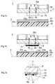
- Figs. 1(a) to 1(c) are schematic illustrations showing an example of the constitution of the apparatus for mounting a semiconductor device of the present invention.
- Fig. 1(a) is an illustration which shows a pressing chip sucked on a compression bonding head.
- Fig. 1(b) is an illustration which shows an IC chip sucked on a compression bonding head.
- Fig. 1(c) is an enlarged view of the part A in Fig. 1(b).
- IC chip 11 to be used in the present invention either an IC chip having bumps or a bumpless one is usable.
- a bumpless IC chip 11 is employed by way of example.
- the mounting apparatus 1 of this embodiment of the present invention is provided with a compression bonding unit 4 having a compression bonding head 2 for pressing the IC chip 11 onto a wiring board 22.
- This compression bonding head 2 which is fixed to the main body (not shown) of the apparatus with a fixture 20, is constructed so that it can be vertically moved against a table 5 on which the wiring board 22 is placed.
- the compression bonding head 2 has a heater (not shown) enclosed therein.
- Plural suction holes 2b are formed on the press face (compression bonding part) 2a of the compression bonding head 2 as will be described hereinafter.
- a hollow suction part 20a is formed in the fixture 20.
- This suction part 20a is connected to the suction hole 2b of the compression bonding head 2 and, on the other hand, also connected to a vacuum pump which is not shown in the drawing. By operating this vacuum pump, the pressure within the suction part 20a is reduced. Thus, the pressing chip 21 or the IC chip 11 is sucked and held on the compression bonding head 2, as Figs. 1(a) and 1(b) show.
- the compression bonding head 2 has such a size as exceeding the largest one among the IC chips 11 and the pressing chips 21 to be sucked thereon.
- the suction holes 2b of the compression bonding head 2 are located on the press face 2a so that the suction holes are involved in the area smaller than the smallest one among the IC chips 11 and the pressing chips 21 to be sucked.
- the area and the number of the suction holes 2b of the compression bonding head 2 are not particularly restricted, it is favorable, from the viewpoint of ensuring the suction of the IC chip 11 or the pressing chip 21, to provide from 1 to 5 suction holes each having a pore area of from 0.01 to 5 mm 2 for one chip.
- the suction holes 2b of the compression bonding head 2 are not particularly restricted in shape. Namely, holes of arbitrary shapes (circular, square, etc.) may be formed.
- a predetermined circuit pattern 14 is formed on an oxide film (SiO 2 ) 13 of a silicone wafer 12, as Fig. 1(c) shows.
- a protective oxide film (a passivation film) 15 provided with a contact hole 16 is further formed on the pad 14a of this circuit pattern 14.
- Figs. 2(a) to 2(c) and Figs. 3(a) to 3(c) are processing diagram showing examples of the process for mounting a semiconductor device of the present invention.
- a conductive particle-free filmy insulating adhesive is first placed on a wiring board 22 having a predetermined circuit pattern formed thereon in such a manner as to cover a connection electrode 22a.
- a compression bonding head 2 heated to about 80°C under, for example, a pressure of 3 kgf/cm 2 for 2 seconds, thereby forming an insulating adhesive layer 23, as shown in Fig. 2(a).
- the insulating adhesive to be used in the present invention has a melt viscosity larger than that of the insulating adhesive 24a in the anisotropic conductive adhesive film 24 as will be described hereinafter.
- this insulating adhesive has a melt viscosity, in particular, a minimum melt viscosity (i.e., the lowest melt viscosity in the state where the viscosity is reduced to the lowest level during the thermocompression bonding) of from 1 x 10 6 to 1 x 10 9 mPa ⁇ s, still preferably from 5 x 10 6 to 5 x 10 8 mPa ⁇ s.
- a minimum melt viscosity i.e., the lowest melt viscosity in the state where the viscosity is reduced to the lowest level during the thermocompression bonding
- the insulating adhesive examples include a mixture of a solid epoxy resin of bisphenol A type with a liquid epoxy resin and a mixture of a thermoplastic resin such as phenoxy resin, acrylic resin, polyester resin, etc. with an epoxy resin.
- the inside of the suction part 20a of the compression bonding head 2 is sucked by driving the vacuum pump as described above.
- the pressing chip 21 is sucked to the press face 2a of the compression bonding head 2.
- the pressing chip 21 is pressed onto a protrusion part (not shown) and the image of the pressing chip 21 is subjected to digital processing, thereby positioning the pressing chip 21.
- the pressing chip 21 it is preferable in the pressing chip 21 to be used in the present invention that at least the face 21a in contact with the insulating adhesive layer 23 is releasable from the insulating adhesive.
- Examples of the pressing chip 21 satisfying the above requirement include a chip prepared by molding polytetrafluoroethylene (PTFE) resin and a chip prepared by release-processing the surface of an aluminum chip with the use of silicone.
- PTFE polytetrafluoroethylene
- the pressing chip 21 has a thickness exceeding the thickness of the insulating adhesive layer 23.
- the thickness of the pressing chip 21 ranges form 0.1 to 5 mm, in case where the thickness of the insulating adhesive layer is from 5 to 100 ⁇ m.
- the pressing chip 21 has a size of 1.5 to 0.5 times, still preferably 1 to 0.7 times to the outer size of the IC chip 11.
- the pressing chip 21 When the pressing chip 21 has a size 0.5 times or less than the outer size of the IC chip 11, there arises a problem that a concave, which will be described hereinafter, is formed inside the electrode (bump) and thus the conductive particles cannot be electrically connected to the electrode.
- the pressing chip 21 has a size 1.5 times or larger than the outer size of the IC chip 11, on the other hand, it becomes impossible to establish the merit of increasing the number of the conductive particles on the pad 14a by blocking the conductive particles or the merit of preventing the conductive particles from reaching the scribe line, as will be described hereinafter.
- thermocompression bonding unit 4 is lowered and hot-press is carried out by using a compression bonding head 2 heated to about 80°C under, for example, a pressure of 3 kgf/cm 2 for 2 seconds, thereby forming a concave 23a having almost the same size as the outer size of the pressing chip 21 in the insulating adhesive layer 23, as shown in Fig. 2(c).
- an anisotropic conductive adhesive film 24 is put into this concave 23a followed by tentative thermocompression bonding, as Fig. 3(a) shows.
- This anisotropic conductive adhesive film 24 has conductive particles 25 dispersed in the insulating adhesive.
- This anisotropic conductive adhesive film 24 is preliminarily cut into a size somewhat smaller than the outer size of the pressing chip 21.
- a brim 23b is formed around the concave 23a by the procedure as described above.
- the height of the brim 23b i.e., the depth of the concave 23a
- the thickness of the IC chip 11 the distance to the bump of the IC chip 11, if formed
- the outer diameter of the conductive particles 25 in the anisotropic conductive adhesive film 24 it is preferable that the height of the brim 23b (i.e., the depth of the concave 23a) is less than the thickness of the IC chip 11 (the distance to the bump of the IC chip 11, if formed) but more than the outer diameter of the conductive particles 25 in the anisotropic conductive adhesive film 24.
- the depth of the concave 23a of the insulating adhesive layer 23 is less than the outer diameter of the conductive particles 25, there arises a problem that the run-off of the conductive particles 25 cannot be sufficiently prevented in the step of the thermocompression bonding.
- the depth is more than the thickness of the IC chip 11, on the other hand, it is feared that the heated compression bonding head 2 might be stained by the insulating adhesive resin squeezed out from the IC chip 11.
- the inner wall of the brim 23b of the concave 23a is located inside the scribe line (not shown) but outside the outmost edge of the pad 14a of the IC chip 11.
- the average particle diameter of the conductive particles 25 ranges from 1 to 10 ⁇ m, still preferably from 2 to 8 ⁇ m.
- the conductive particles 25 are dispersed in the insulating adhesive at a ratio of from 1 to 15% by volume, still preferably from 3 to 15% by volume.
- the content of the conductive particles 25 is less than 1% by volume, there arises a problem that the electrical connection between the pad 14a of the IC chip 11 and the connection electrode 22a of the wiring board 22 cannot be surely established and thus the conduction resistance is increased.
- the content of the conductive particles 25 exceeds 15% by volume, on the other hand, there arises another problem that the conductive particles 25 aggregate together and thus the insulation resistance between electrodes adjacent to each other is lowered.
- the concave 23a is formed in the insulating adhesive layer 23 with the use of the pressing chip 21. Then the operation with the vacuum pump is stopped and thus the pressing chip 21 is stripped from the compression bonding head 2. Subsequently, the IC chip 11 is sucked onto the press face 2a of the compression bonding head 2, as Fig. 3(b) shows, and the IC chip 11 is positioned as in the case of the pressing chip 21.
- the compression bonding unit 4 is lowered and the IC chip 11 is thermocompression bonded by using the compression bonding head 2 heated to about 180°C under a pressure of, for example, 1000 kgf/cm 2 for 20 seconds, as Fig. 3(c) shows.
- the anisotropic conductive adhesive film 24 and the insulating adhesive layer 23 are crushed by the IC chip 11.
- the conductive particles 25 come into contact with the connection electrode 22a of the wiring board 22 and the pad 14a of the IC chip 11 and thus the IC chip 11 is electrically connected to the wiring board 22.
- the conductive particles 25 tending to run-off toward the edge of the IC chip 11 are blocked by the brim 23b of the concave 23a formed in the insulating adhesive layer 23.
- the conductive particles scarcely flow toward the edge of the IC chip 11.
- the conductive particles 25 can be densely held between the IC chip 11 and the wiring board 22.
- plural conductive particles 25 can be provided on the connection electrode 22a of the wiring board 22 and the pad 14a of the IC chip 11 at an extremely high probability so as to electrically connect the connection electrode to the IC chip without fail even in a case where the connection electrodes are located at very small intervals.
- the IC chip 11 and the pressing chip 21 are removable from the compression bonding head 2. Owing to this construction, it is unnecessary to provide an additional press head for forming the concave, which contributes to the simplification and down-sizing of the mounting apparatus 1.
- the IC chip 11 and the pressing chip 21 are sucked onto the compression bonding head 2 by sucking the air.
- the IC chip 11, etc. can be easily and quickly attached and removed by switching the suction.
- at least the face 21 in contact with the insulating adhesive layer 23 is releasable from the insulating adhesive. Owing to this construction, the releasable press face 21a of pressing chip 21 prevent stripping the insulating adhesive layer 23 from the wiring board 22 caused by adhering to the pressing chip 21.
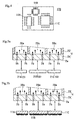
- Fig. 4 is a plan view showing an example of a wiring board having IC chips of various types mounted thereon (a multi chip module).
- Fig. 5 is a schematic illustration showing the main part of another embodiment of the present invention.
- Fig. 4 shows, three types of IC chips 11A, 11B and 11C differing in outer shape from each other are mounted on this wiring board 220.
- Each suction part 20a formed in the fixture 20 of the main body of the apparatus is connected to the suction hole 2b of the compression bonding head and, on the other hand, also connected to a vacuum pump (not shown), as in the case of the above-described embodiment of the present invention.
- first to third pressing chips 21A, 21B and 21C each satisfying the requirements as described above, and anisotropic conductive adhesive films (not shown) are prepared respectively for the IC chips 11A, 11B and 11C.
- the first to third pressing chips 21 are sucked on the compression bonding head 2A of the mounting apparatus, as shown in Fig. 5(a).
- concaves are formed in the insulating adhesive layer as in the above-described process and then the pressing chips 21A, 21B and 21C are stripped from the compression bonding head 2A.
- the first to third IC chips 11A to 11C are sucked onto the compression bonding head 2 and subjected to thermocompression bonding. Next, the first to third IC chips 11 are stripped from the compression bonding head 2A.
- the first to third pressing chips 21A, 21B and 21C and the first to third IC chips 11A, 11B and 11C are attached and removed from the single compression bonding head.
- the apparatus constitution can be simplified and down-sized.
- a single compression bonding head from which pressing chips and IC chips are removable.
- the present invention is not restricted to this case but use can be made of, for example, heads respectively for sucking pressing chips and IC chips.
- heads respectively for sucking pressing chips and IC chips.
- it is favorable to construct that pressing chips and IC chips are removable from a single compression bonding head.
- the present invention is also applicable to mounting of semiconductor devices having bumps in various shapes.
- a rigid substrate obtained by forming a copper (Cu) pattern (width: 18 ⁇ m, pitch: 150 ⁇ m) on a heat-resistant glass cloth base epoxy resin copper clad laminate (FR-4) of 0.7 mm in thickness followed by plating with nickel/gold.
- IC chips chip A (6 mm x 6mm), chip B (3 mm x 6 mm) and chip C (3.3 mm x 3.3 mm) provided with electrodes of 150 ⁇ m pitch (bumpless) were prepared.
- chip (1) (5.7 mm x 5.7 mm)
- chip (2) (2.7 mm x 5.7 mm)
- chip (3) (3.0 mm x 3.0 mm) made of polytetrafluoroethylene (PTFE) resin with a thickness of 1 mm were employed as the pressing chips.
- PTFE polytetrafluoroethylene
- anisotropic conductive adhesive film use was made of SCFP20626 TM (manufactured by SONY CHEMICALS).
- conductive particle-free insulating adhesive use was made of a film (thickness 15 ⁇ m) obtained by removing conductive particles from the above-described SCFP20626 TM (manufactured by SONY CHEMICALS).
- the conductive particle-free insulating adhesive film was cut into pieces corresponding to the IC chips A to C and then tentatively thermocompression bonded at 80°C under a pressure of 3 kgf/cm 2 for 2 seconds.
- thermocompression bonding was performed at 180°C under a pressure of 1000 kgf/cm 2 /bump for 20 seconds.
- connection was performed by using an anisotropic conductive adhesive film as in Example 1 but using a chip (3.0 mm x 3.0 mm) made of silicone-surface-processed aluminum (thickness: 1 mm) as the pressing chip.
- connection was performed by using an anisotropic conductive adhesive film as in Example 1 but using a chip (3.0 mm x 3.0 mm) made of aluminum (thickness: 1 mm) as the pressing chip.
- the maximal initial resistance was 15 m ⁇ or less in each case.
- the maximal resistance was 50 m ⁇ or less in each case, thus showing good conduction reliability.
- connection electrodes plural conductive particles can be provided on each connection electrode at an extremely high probability and connection electrodes can be surely electrically connected to each other without fail even in a case where the connection electrodes are located at very small intervals, as described above.
- IC chips of various types can be mounted on a wiring board within a short time without resort to a complicated and large-sized apparatus constitution.
Landscapes
- Engineering & Computer Science (AREA)
- Manufacturing & Machinery (AREA)
- Microelectronics & Electronic Packaging (AREA)
- Wire Bonding (AREA)
- Adhesive Tapes (AREA)
Applications Claiming Priority (2)
| Application Number | Priority Date | Filing Date | Title |
|---|---|---|---|
| JP22527599 | 1999-08-09 | ||
| JP22527599A JP3372511B2 (ja) | 1999-08-09 | 1999-08-09 | 半導体素子の実装方法及び実装装置 |
Publications (2)
| Publication Number | Publication Date |
|---|---|
| EP1076360A2 true EP1076360A2 (de) | 2001-02-14 |
| EP1076360A3 EP1076360A3 (de) | 2005-02-02 |
Family
ID=16826784
Family Applications (1)
| Application Number | Title | Priority Date | Filing Date |
|---|---|---|---|
| EP00116898A Withdrawn EP1076360A3 (de) | 1999-08-09 | 2000-08-04 | Halbleitermontagemethode und Montageapparat |
Country Status (4)
| Country | Link |
|---|---|
| US (2) | US6340607B1 (de) |
| EP (1) | EP1076360A3 (de) |
| JP (1) | JP3372511B2 (de) |
| KR (1) | KR100616792B1 (de) |
Families Citing this family (27)
| Publication number | Priority date | Publication date | Assignee | Title |
|---|---|---|---|---|
| AU2001293125A1 (en) * | 2000-09-27 | 2002-04-08 | Strasbaugh, Inc. | Tool for applying resilient tape to chuck used for grinding or polishing wafers |
| JP3851767B2 (ja) * | 2000-10-16 | 2006-11-29 | ソニーケミカル&インフォメーションデバイス株式会社 | 接着フィルム、及び接着フィルムの製造方法 |
| JP2002299595A (ja) * | 2001-04-03 | 2002-10-11 | Matsushita Electric Ind Co Ltd | 固体撮像装置およびその製造方法 |
| JP4116851B2 (ja) * | 2002-09-19 | 2008-07-09 | 富士通株式会社 | 電子部品の処理方法及び電子部品用治具 |
| US7456050B2 (en) * | 2003-07-01 | 2008-11-25 | Stmicroelectronics, Inc. | System and method for controlling integrated circuit die height and planarity |
| JP5196703B2 (ja) * | 2004-01-15 | 2013-05-15 | デクセリアルズ株式会社 | 接着フィルム |
| TWI275437B (en) * | 2005-06-30 | 2007-03-11 | Fujitsu Ltd | Method and device for removing micro component |
| US20080197465A1 (en) * | 2007-02-20 | 2008-08-21 | Matsushita Electric Industrial Co., Ltd. | Semiconductor device and method of manufacturing the same |
| EP1978559A3 (de) * | 2007-04-06 | 2013-08-28 | Hitachi, Ltd. | Halbleiterbauelement |
| JP5186157B2 (ja) * | 2007-08-24 | 2013-04-17 | デクセリアルズ株式会社 | 異方性導電フィルム及びそれを用いた接続構造体の製造方法 |
| JP4897778B2 (ja) * | 2008-11-20 | 2012-03-14 | ソニーケミカル&インフォメーションデバイス株式会社 | 接続フィルム、並びに、接合体及びその製造方法 |
| JP2011018873A (ja) * | 2009-05-22 | 2011-01-27 | Sony Ericsson Mobilecommunications Japan Inc | 電磁シールド方法および電磁シールド用フィルム |
| US20120267423A1 (en) * | 2011-04-19 | 2012-10-25 | Taiwan Semiconductor Manufacturing Company, Ltd. | Methods and Apparatus for Thin Die Processing |
| US8426227B1 (en) | 2011-11-18 | 2013-04-23 | LuxVue Technology Corporation | Method of forming a micro light emitting diode array |
| US8349116B1 (en) | 2011-11-18 | 2013-01-08 | LuxVue Technology Corporation | Micro device transfer head heater assembly and method of transferring a micro device |
| US9773750B2 (en) * | 2012-02-09 | 2017-09-26 | Apple Inc. | Method of transferring and bonding an array of micro devices |
| KR101526278B1 (ko) * | 2012-12-21 | 2015-06-05 | 제일모직주식회사 | 경화 필름과 도전 필름을 포함하는 분리형 이방 도전성 필름 |
| JP5874683B2 (ja) * | 2013-05-16 | 2016-03-02 | ソニー株式会社 | 実装基板の製造方法、および電子機器の製造方法 |
| JP2015053418A (ja) * | 2013-09-09 | 2015-03-19 | 株式会社東芝 | 半導体製造装置 |
| KR102107456B1 (ko) | 2013-12-10 | 2020-05-08 | 삼성디스플레이 주식회사 | 플렉시블 표시 장치 및 이의 제조 방법 |
| GB2524791B (en) | 2014-04-02 | 2018-10-03 | At & S Austria Tech & Systemtechnik Ag | Placement of component in circuit board intermediate product by flowable adhesive layer on carrier substrate |
| KR20160046977A (ko) * | 2014-10-20 | 2016-05-02 | 삼성디스플레이 주식회사 | 이방성 도전입자 |
| JP6582975B2 (ja) | 2015-12-28 | 2019-10-02 | 富士通株式会社 | 半導体実装装置、半導体実装装置のヘッド及び積層チップの製造方法 |
| US11049839B2 (en) | 2018-01-24 | 2021-06-29 | Kulicke And Soffa Industries, Inc. | Bonding tools for bonding machines, bonding machines for bonding semiconductor elements, and related methods |
| JP7024464B2 (ja) * | 2018-02-02 | 2022-02-24 | 浜名湖電装株式会社 | 電気部品製造装置および電気部品の製造方法 |
| CN108807717B (zh) * | 2018-08-14 | 2019-11-15 | 武汉华星光电半导体显示技术有限公司 | 一种显示面板及绑定方法 |
| KR20210019323A (ko) * | 2019-08-12 | 2021-02-22 | 삼성전자주식회사 | 마이크로 엘이디 디스플레이 및 이의 제작 방법 |
Family Cites Families (24)
| Publication number | Priority date | Publication date | Assignee | Title |
|---|---|---|---|---|
| JPS5412266A (en) * | 1977-06-28 | 1979-01-29 | Mitsubishi Electric Corp | Compression bonding device of metal foils and pieces |
| JPS5669839A (en) * | 1979-11-12 | 1981-06-11 | Toshiba Corp | Semiconductor device and manufacture thereof |
| JPS57164538A (en) * | 1981-04-02 | 1982-10-09 | Toshiba Corp | Die bonding device for semiconductor |
| JPS5831541A (ja) * | 1981-08-19 | 1983-02-24 | Toshiba Corp | 箔供給装置 |
| JP2955435B2 (ja) * | 1992-12-01 | 1999-10-04 | 株式会社東芝 | マウント装置 |
| KR0146063B1 (ko) * | 1995-03-28 | 1998-08-01 | 문정환 | 반도체 패키지 및 그 제조방법 |
| US6008072A (en) * | 1995-12-27 | 1999-12-28 | Industrial Technology Research Institute | Tape automated bonding method |
| JPH1084014A (ja) * | 1996-07-19 | 1998-03-31 | Shinko Electric Ind Co Ltd | 半導体装置の製造方法 |
| JP2848357B2 (ja) * | 1996-10-02 | 1999-01-20 | 日本電気株式会社 | 半導体装置の実装方法およびその実装構造 |
| US5985064A (en) * | 1996-11-28 | 1999-11-16 | Matsushita Electric Industrial Co., Ltd. | Chip compression-bonding apparatus and method |
| US5757073A (en) * | 1996-12-13 | 1998-05-26 | International Business Machines Corporation | Heatsink and package structure for wirebond chip rework and replacement |
| JPH10270496A (ja) * | 1997-03-27 | 1998-10-09 | Hitachi Ltd | 電子装置、情報処理装置、半導体装置並びに半導体チップの実装方法 |
| JPH10313161A (ja) * | 1997-05-12 | 1998-11-24 | Hitachi Chem Co Ltd | 配線基板 |
| JP3725300B2 (ja) * | 1997-06-26 | 2005-12-07 | 松下電器産業株式会社 | Acf接合構造 |
| JPH1197487A (ja) * | 1997-09-25 | 1999-04-09 | Toshiba Corp | 実装方法及びその装置及び異方性導電シート |
| JPH11126794A (ja) * | 1997-10-22 | 1999-05-11 | Toshiba Corp | 実装回路装置の製造方法 |
| US6204454B1 (en) * | 1997-12-27 | 2001-03-20 | Tdk Corporation | Wiring board and process for the production thereof |
| JP3317226B2 (ja) * | 1998-01-16 | 2002-08-26 | ソニーケミカル株式会社 | 熱圧着装置 |
| US6037192A (en) * | 1998-01-22 | 2000-03-14 | Nortel Networks Corporation | Process of assembling an integrated circuit and a terminal substrate using solder reflow and adhesive cure |
| JP3424735B2 (ja) * | 1998-05-19 | 2003-07-07 | ソニーケミカル株式会社 | 粒状異方性導電接着剤 |
| JP3405269B2 (ja) * | 1999-04-26 | 2003-05-12 | ソニーケミカル株式会社 | 実装方法 |
| JP3325000B2 (ja) * | 1999-05-28 | 2002-09-17 | ソニーケミカル株式会社 | 半導体素子の実装方法 |
| JP3402267B2 (ja) * | 1999-06-23 | 2003-05-06 | ソニーケミカル株式会社 | 電子素子の実装方法 |
| EP1187181A3 (de) * | 2000-09-12 | 2002-04-10 | Esec Trading S.A. | Verfahren und Vorrichtung für die Montage von Halbleiterchips |
-
1999
- 1999-08-09 JP JP22527599A patent/JP3372511B2/ja not_active Expired - Fee Related
-
2000
- 2000-08-03 US US09/631,282 patent/US6340607B1/en not_active Expired - Fee Related
- 2000-08-03 KR KR1020000044982A patent/KR100616792B1/ko not_active Expired - Fee Related
- 2000-08-04 EP EP00116898A patent/EP1076360A3/de not_active Withdrawn
-
2001
- 2001-08-14 US US09/928,516 patent/US6769469B2/en not_active Expired - Lifetime
Non-Patent Citations (1)
| Title |
|---|
| None * |
Also Published As
| Publication number | Publication date |
|---|---|
| JP3372511B2 (ja) | 2003-02-04 |
| JP2001053110A (ja) | 2001-02-23 |
| US20020029857A1 (en) | 2002-03-14 |
| EP1076360A3 (de) | 2005-02-02 |
| KR20010039786A (ko) | 2001-05-15 |
| US6769469B2 (en) | 2004-08-03 |
| KR100616792B1 (ko) | 2006-08-29 |
| US6340607B1 (en) | 2002-01-22 |
Similar Documents
| Publication | Publication Date | Title |
|---|---|---|
| US6340607B1 (en) | Process for mounting semiconductor device and mounting apparatus | |
| US6409866B1 (en) | Process for mounting semiconductor device | |
| US6370032B1 (en) | Compliant microelectronic mounting device | |
| US7582512B2 (en) | Method of fabricating semiconductor device having conducting portion of upper and lower conductive layers on a peripheral surface of the semiconductor device | |
| JP3569511B2 (ja) | 半導体装置の実装構造、その実装方法および液晶表示パネル | |
| KR100781827B1 (ko) | 반도체 패키지 및 그 제조 방법 | |
| US7687319B2 (en) | Semiconductor device and manufacturing method thereof | |
| EP1310992A1 (de) | Mikropartikelanordnungsfilm, elektrischer verbindungsfilm, elektrische verbindungsstruktur und mikropartikelanordnungsverfahren | |
| US9490224B2 (en) | Semiconductor device and manufacturing method thereof | |
| US6137162A (en) | Chip stack package | |
| KR20000023622A (ko) | 반도체 패키지의 제조 방법 및 집합 회로 기판 | |
| EP0527387A1 (de) | Verfahrungen und Vorrichtung zur Befestigung von Kontakthöckern auf TAB-Trägerleiter | |
| KR0129119B1 (ko) | 반도체칩의 제거방법 및 제거장치 | |
| US20070243667A1 (en) | POP Semiconductor Device Manufacturing Method | |
| KR20010069987A (ko) | 반도체 장치 | |
| JP3514649B2 (ja) | フリップチップ接続構造および接続方法 | |
| JP2001345560A (ja) | 配線基板およびその製造方法、並びに電子部品 | |
| US6821813B2 (en) | Process for bonding solder bumps to a substrate | |
| KR100225398B1 (ko) | 반도체 범프의 본딩구조 및 방법 | |
| JPH05267393A (ja) | 半導体装置及びその製造方法 | |
| JP4770195B2 (ja) | 半導体装置の製造方法 | |
| US20240090130A1 (en) | Leadframe mounting with lead insertion for lead wall bonding | |
| JP3964515B2 (ja) | 半導体装置の切断分離方法 | |
| JP4369631B2 (ja) | 多数個取り配線基板 | |
| JP2003059978A (ja) | 電子部品実装用フィルムキャリアテープの製造方法及び製造装置 |
Legal Events
| Date | Code | Title | Description |
|---|---|---|---|
| PUAI | Public reference made under article 153(3) epc to a published international application that has entered the european phase |
Free format text: ORIGINAL CODE: 0009012 |
|
| AK | Designated contracting states |
Kind code of ref document: A2 Designated state(s): AT BE CH CY DE DK ES FI FR GB GR IE IT LI LU MC NL PT SE |
|
| AX | Request for extension of the european patent |
Free format text: AL;LT;LV;MK;RO;SI |
|
| PUAL | Search report despatched |
Free format text: ORIGINAL CODE: 0009013 |
|
| AK | Designated contracting states |
Kind code of ref document: A3 Designated state(s): AT BE CH CY DE DK ES FI FR GB GR IE IT LI LU MC NL PT SE |
|
| AX | Request for extension of the european patent |
Extension state: AL LT LV MK RO SI |
|
| 17P | Request for examination filed |
Effective date: 20050603 |
|
| AKX | Designation fees paid |
Designated state(s): DE FR GB NL |
|
| 17Q | First examination report despatched |
Effective date: 20061228 |
|
| STAA | Information on the status of an ep patent application or granted ep patent |
Free format text: STATUS: THE APPLICATION IS DEEMED TO BE WITHDRAWN |
|
| 18D | Application deemed to be withdrawn |
Effective date: 20140301 |