EP1094519A1 - Leiterrahmen für halbleiteranordnung - Google Patents
Leiterrahmen für halbleiteranordnung Download PDFInfo
- Publication number
- EP1094519A1 EP1094519A1 EP00911362A EP00911362A EP1094519A1 EP 1094519 A1 EP1094519 A1 EP 1094519A1 EP 00911362 A EP00911362 A EP 00911362A EP 00911362 A EP00911362 A EP 00911362A EP 1094519 A1 EP1094519 A1 EP 1094519A1
- Authority
- EP
- European Patent Office
- Prior art keywords
- copper
- plating film
- lead frame
- alloy
- zinc
- Prior art date
- Legal status (The legal status is an assumption and is not a legal conclusion. Google has not performed a legal analysis and makes no representation as to the accuracy of the status listed.)
- Withdrawn
Links
Images

Classifications
-
- H—ELECTRICITY
- H10—SEMICONDUCTOR DEVICES; ELECTRIC SOLID-STATE DEVICES NOT OTHERWISE PROVIDED FOR
- H10W—GENERIC PACKAGES, INTERCONNECTIONS, CONNECTORS OR OTHER CONSTRUCTIONAL DETAILS OF DEVICES COVERED BY CLASS H10
- H10W72/00—Interconnections or connectors in packages
-
- H—ELECTRICITY
- H10—SEMICONDUCTOR DEVICES; ELECTRIC SOLID-STATE DEVICES NOT OTHERWISE PROVIDED FOR
- H10W—GENERIC PACKAGES, INTERCONNECTIONS, CONNECTORS OR OTHER CONSTRUCTIONAL DETAILS OF DEVICES COVERED BY CLASS H10
- H10W70/00—Package substrates; Interposers; Redistribution layers [RDL]
- H10W70/40—Leadframes
- H10W70/456—Materials
- H10W70/457—Materials of metallic layers on leadframes
-
- H—ELECTRICITY
- H10—SEMICONDUCTOR DEVICES; ELECTRIC SOLID-STATE DEVICES NOT OTHERWISE PROVIDED FOR
- H10W—GENERIC PACKAGES, INTERCONNECTIONS, CONNECTORS OR OTHER CONSTRUCTIONAL DETAILS OF DEVICES COVERED BY CLASS H10
- H10W72/00—Interconnections or connectors in packages
- H10W72/071—Connecting or disconnecting
- H10W72/075—Connecting or disconnecting of bond wires
-
- H—ELECTRICITY
- H10—SEMICONDUCTOR DEVICES; ELECTRIC SOLID-STATE DEVICES NOT OTHERWISE PROVIDED FOR
- H10W—GENERIC PACKAGES, INTERCONNECTIONS, CONNECTORS OR OTHER CONSTRUCTIONAL DETAILS OF DEVICES COVERED BY CLASS H10
- H10W72/00—Interconnections or connectors in packages
- H10W72/50—Bond wires
-
- H—ELECTRICITY
- H10—SEMICONDUCTOR DEVICES; ELECTRIC SOLID-STATE DEVICES NOT OTHERWISE PROVIDED FOR
- H10W—GENERIC PACKAGES, INTERCONNECTIONS, CONNECTORS OR OTHER CONSTRUCTIONAL DETAILS OF DEVICES COVERED BY CLASS H10
- H10W72/00—Interconnections or connectors in packages
- H10W72/851—Dispositions of multiple connectors or interconnections
- H10W72/874—On different surfaces
- H10W72/884—Die-attach connectors and bond wires
-
- H—ELECTRICITY
- H10—SEMICONDUCTOR DEVICES; ELECTRIC SOLID-STATE DEVICES NOT OTHERWISE PROVIDED FOR
- H10W—GENERIC PACKAGES, INTERCONNECTIONS, CONNECTORS OR OTHER CONSTRUCTIONAL DETAILS OF DEVICES COVERED BY CLASS H10
- H10W72/00—Interconnections or connectors in packages
- H10W72/90—Bond pads, in general
- H10W72/951—Materials of bond pads
-
- H—ELECTRICITY
- H10—SEMICONDUCTOR DEVICES; ELECTRIC SOLID-STATE DEVICES NOT OTHERWISE PROVIDED FOR
- H10W—GENERIC PACKAGES, INTERCONNECTIONS, CONNECTORS OR OTHER CONSTRUCTIONAL DETAILS OF DEVICES COVERED BY CLASS H10
- H10W72/00—Interconnections or connectors in packages
- H10W72/90—Bond pads, in general
- H10W72/951—Materials of bond pads
- H10W72/952—Materials of bond pads comprising metals or metalloids, e.g. PbSn, Ag or Cu
-
- H—ELECTRICITY
- H10—SEMICONDUCTOR DEVICES; ELECTRIC SOLID-STATE DEVICES NOT OTHERWISE PROVIDED FOR
- H10W—GENERIC PACKAGES, INTERCONNECTIONS, CONNECTORS OR OTHER CONSTRUCTIONAL DETAILS OF DEVICES COVERED BY CLASS H10
- H10W74/00—Encapsulations, e.g. protective coatings
-
- H—ELECTRICITY
- H10—SEMICONDUCTOR DEVICES; ELECTRIC SOLID-STATE DEVICES NOT OTHERWISE PROVIDED FOR
- H10W—GENERIC PACKAGES, INTERCONNECTIONS, CONNECTORS OR OTHER CONSTRUCTIONAL DETAILS OF DEVICES COVERED BY CLASS H10
- H10W90/00—Package configurations
- H10W90/701—Package configurations characterised by the relative positions of pads or connectors relative to package parts
- H10W90/731—Package configurations characterised by the relative positions of pads or connectors relative to package parts of die-attach connectors
- H10W90/736—Package configurations characterised by the relative positions of pads or connectors relative to package parts of die-attach connectors between a chip and a stacked lead frame, conducting package substrate or heat sink
-
- H—ELECTRICITY
- H10—SEMICONDUCTOR DEVICES; ELECTRIC SOLID-STATE DEVICES NOT OTHERWISE PROVIDED FOR
- H10W—GENERIC PACKAGES, INTERCONNECTIONS, CONNECTORS OR OTHER CONSTRUCTIONAL DETAILS OF DEVICES COVERED BY CLASS H10
- H10W90/00—Package configurations
- H10W90/701—Package configurations characterised by the relative positions of pads or connectors relative to package parts
- H10W90/751—Package configurations characterised by the relative positions of pads or connectors relative to package parts of bond wires
- H10W90/756—Package configurations characterised by the relative positions of pads or connectors relative to package parts of bond wires between a chip and a stacked lead frame, conducting package substrate or heat sink
-
- Y—GENERAL TAGGING OF NEW TECHNOLOGICAL DEVELOPMENTS; GENERAL TAGGING OF CROSS-SECTIONAL TECHNOLOGIES SPANNING OVER SEVERAL SECTIONS OF THE IPC; TECHNICAL SUBJECTS COVERED BY FORMER USPC CROSS-REFERENCE ART COLLECTIONS [XRACs] AND DIGESTS
- Y10—TECHNICAL SUBJECTS COVERED BY FORMER USPC
- Y10T—TECHNICAL SUBJECTS COVERED BY FORMER US CLASSIFICATION
- Y10T29/00—Metal working
- Y10T29/49—Method of mechanical manufacture
- Y10T29/49002—Electrical device making
- Y10T29/49117—Conductor or circuit manufacturing
- Y10T29/49169—Assembling electrical component directly to terminal or elongated conductor
- Y10T29/49171—Assembling electrical component directly to terminal or elongated conductor with encapsulating
- Y10T29/49172—Assembling electrical component directly to terminal or elongated conductor with encapsulating by molding of insulating material
-
- Y—GENERAL TAGGING OF NEW TECHNOLOGICAL DEVELOPMENTS; GENERAL TAGGING OF CROSS-SECTIONAL TECHNOLOGIES SPANNING OVER SEVERAL SECTIONS OF THE IPC; TECHNICAL SUBJECTS COVERED BY FORMER USPC CROSS-REFERENCE ART COLLECTIONS [XRACs] AND DIGESTS
- Y10—TECHNICAL SUBJECTS COVERED BY FORMER USPC
- Y10T—TECHNICAL SUBJECTS COVERED BY FORMER US CLASSIFICATION
- Y10T29/00—Metal working
- Y10T29/49—Method of mechanical manufacture
- Y10T29/49002—Electrical device making
- Y10T29/49117—Conductor or circuit manufacturing
- Y10T29/49204—Contact or terminal manufacturing
- Y10T29/49208—Contact or terminal manufacturing by assembling plural parts
- Y10T29/4922—Contact or terminal manufacturing by assembling plural parts with molding of insulation
Definitions
- the present invention relates to a semiconductor device lead frame, a process of production of the same, a semiconductor device using the lead frame, and a process of production of the same.
- a semiconductor device lead frame used in a resin sealing type semiconductor device is made using, other than an iron-nickel-based alloy (representatively Fe-42% Ni alloy), a copper-based material made of copper or a copper alloy.
- a copper strike plating film is formed on the surface of the material, then the above precious metal plating film for improving die bonding and wire bonding is formed on a die pad and on wire bonding portions of inner leads.
- the material is a copper alloy
- a segregation layer is formed by the additional element of the copper alloy (layer due to the oxide of the additional element) at an interface between the formed oxide film of copper and the copper alloy material, and the oxide film of the copper ends up being peeled off together with this segregation layer.
- This is caused by the large difference in density between the copper oxide film and segregation layer and the copper alloy material and therefore mismatching or incoherency at the interface.
- the semiconductor device is finally completed, a problem arises in the adhesion with the sealing resin.
- Japanese Examined Patent Publication (Kokoku) No. 5-19820 proposes a semiconductor device lead frame comprised of a lead frame material made of copper or a copper alloy on which is formed a copper-zinc alloy plating film serving as an under plating of the precious metal plating (silver plating).
- the zinc of the copper-zinc plating film acts as a barrier against diffusion of the oxygen from the outside and suppress the formation of the segregation layer, whereby a semiconductor device lead frame excellent in adhesion with the sealing resin is obtained.
- An object of the present invention is to provide a semiconductor device lead frame excellent in an adhesion with a sealing resin, free from contamination of a precious metal plating solution (particularly a silver plating solution), having a good appearance of the precious metal plating film, excellent in corrosion resistance and moisture resistance, and having a good appearance and adhesion of an outer lead solder plating film, a process of production of the same, a semiconductor device using the lead frame, and a process of production of the same.
- a semiconductor device lead frame made of copper or a copper alloy and used for a resin sealing type semiconductor device comprising:
- a semiconductor device lead frame made of copper or a copper alloy and used for a resin sealing type semiconductor device comprising:
- a double-layer under plating film consisting of a lower layer made of zinc or a copper-zinc alloy and an upper layer made of copper having a thickness of 0.02 to 0.4 ⁇ m.
- the thickness of the copper upper layer provided on the zinc or the copper-zinc alloy lower layer is at least 0.02 ⁇ m, formation of an oxide film at the interface between the under plating film and the lead frame material can be prevented. Namely, in the heat treatment when mounting the semiconductor chip, the copper plating film at the surface layer is oxidized, but after the zinc or the copper-zinc alloy plating film is oxidized, oxygen will no longer reach the copper alloy material of the lead frame body, oxidation of the material will be greatly suppressed, and, as a result, no segregation layer of the additional element of the alloy (layer of the oxide of the alloy element) will be formed, so that the peeling of the oxide film and the interface of the material can be prevented.
- the zinc or the copper-zinc alloy plating film of the lower layer is covered by the copper plating film of the upper layer and therefore is not exposed. Due to this, the following effects 1) to 3) are further obtained in addition to the effect described above.
- the under plating film can be completely removed by washing by an acid before the external solder plating of the outer leads (after washing by an alkali to remove the resin flashes), therefore no under plating film will remain and lower the appearance and the adhesion of the solder plating film.
- the bonding structure [Cu/Zn/Sn-Pb] obtained as a result of this has a low bonding strength at the Cu/Zn interface and the Zn/Sn-Pb interface, so the solder bonding strength is lowered.
- the standard practice is to use sulfuric acid or another acid having a concentration of about 10 to 15 v/v% and a pH of about 1. With an acid weaker than this, the removal time becomes extremely long, while with an acid stronger than this, the surface of the outer leads become rough, so neither are practical.
- the thickness of the copper upper layer is further desirably set at 0.1 to 0.3 ⁇ m by which the above effects are obtained most stably.
- the zinc or zinc alloy lower layer is made thick enough to prevent the oxidation at the interface between the copper or copper alloy material and the under plating film and thin enough to be easily removed by the acid washing before the outer lead solder plating.
- the lower layer can be formed as a strike plating film having a thickness of about 0.001 to 0.5 ⁇ m, desirably about 0.01 ⁇ m.
- a double-layer under plating film comprised of a lower layer made of one type of metal selected from among silver, tin, iron, cadmium, copper-nickel alloy, and copper-cadmium and an upper layer made of copper
- the metal of the lower layer has a higher corrosion resistance and oxidation resistance than zinc and does not leach out much into acid, so the thickness of the copper upper layer can be reduced from that in the first aspect of the invention.
- the thickness of the copper upper layer is set at 0.1 to 0.3 ⁇ m.
- the lower layer can be formed as a strike plating film having a thickness of about 0.001 to 0.5 ⁇ m, desirably about 0.01 ⁇ m, from the same viewpoint as the first aspect of the invention.
- a semiconductor device lead frame made of copper or a copper alloy and used for a resin sealing type semiconductor device comprising:
- a copper-nickel alloy and a copper-cadmium alloy particularly have a high corrosion resistance and oxidation resistance and do not leach out much into an acid, therefore can be formed as the under plating film without the copper upper layer.
- the adhesion of the oxide film formed at the interface with the precious metal plating film is somewhat low, so it is desirable to suitably select the application.
- the under plating film can be formed as a strike plating film having a thickness of about 0.001 to 0.5 ⁇ m, desirably about 0.01 ⁇ m, from the same viewpoint as the lower layer of the first aspect of the invention.
- the process of production of a semiconductor device lead frame of the first aspect of the present invention comprises:
- the thickness of the upper layer copper plating film is most desirably 0.1 ⁇ m to 0.3 ⁇ m from the same viewpoint as the first aspect of the invention.
- the zinc or the copper-zinc alloy lower layer can be formed as a strike plating film having a thickness of about 0.001 to 0.5 ⁇ m, desirably about 0.01 ⁇ m, from the same viewpoint as the first aspect of the invention.
- a semiconductor device using a lead frame of the first, second, or third aspect of the invention is formed by mounting a semiconductor chip on a lead frame, electrically connecting the semiconductor chip and the wire bonding portions of said inner leads by bonding wires, and sealing said semiconductor chip by a resin.
- the under plating film on the outer leads of the lead frame is removed (peeled off), and the solder plating film is formed on the exposed outer leads.
- the process of production of a semiconductor device using a lead frame of the first aspect of the invention comprises:
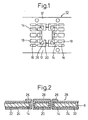
- a copper-based material 8 is pressed or etched to form a lead frame body 10 having a frame 12, inner leads 14, outer leads 16, tie bars 18, and a die pad 20.
- the copper-based material use can be made of various materials such as pure copper, a copper-tin alloy, a copper-zinc alloy, a copper-iron alloy, and a copper-chromium alloy.
- the zinc plating film 22 is formed as a strike plating film having a thickness of about 0.001 to 0.5 ⁇ m, desirably about 0.01 ⁇ m.
- a copper plating film 24 having a thickness of 0.02 to 0.4 ⁇ m is formed on this zinc plating film 22.
- the thickness of the copper plating film 24 is further desirably 0.1 to 0.3 ⁇ m.
- a precious metal plating film 26 made of silver, gold, palladium, a double layer of lower layer palladium/upper layer gold, or the like is formed on the die pad 20 of the lead frame body 10 and the wire bonding portions of the inner leads 14 to complete a semiconductor device lead frame 28. Note that, it is not always necessary to form the precious metal plating film 26 on the die pad 20.
- a semiconductor chip 30 is mounted on the semiconductor device lead frame 28 by using an adhesive 32, the semiconductor chip 30 and the wire bonding portions of the inner leads 14 are electrically connected by bonding wires 34, and the semiconductor chip 30 is sealed by a sealing resin 36, whereby a semiconductor device 38 was completed.
- the adhesion with the sealing resin when completing the semiconductor device was also good.
- reference numeral 40 is an external solder plating film formed on the outer leads 16.
- This external solder plating film 40 may be directly formed on the outer leads 16 exposed by peeling off the copper plating film 24 and the zinc plating film 22 from the outer leads 16.
- the peeling by the peeling solution can be easily and completely carried out.
- the zinc plating film 22 of the lower layer is very thin as described above, so this also can be easily peeled off. Since the under plating film can be completely peeled in this way, a solder plating film 40 can be formed with a good adhesion and good appearance.
- composition of the zinc plating solution and plating conditions is shown below:
- composition of the copper plating solution and plating conditions is shown below:
- a zinc plating film of 0.01 ⁇ m was formed on a copper alloy material (Cu and 1 to 3 wt% Sn alloy, same below) using the above plating solution. Copper plating films having thicknesses of 0.1 ⁇ m, 0.3 ⁇ m, and 0.4 ⁇ m were formed on such a zinc plating film using the above plating solution.
- a copper-zinc alloy plating film 22 is formed in place of the zinc plating film 22 on the lead frame body 10. Also, a copper-zinc alloy plating film is formed as a strike plating film having a thickness of about 0.001 to 0.5 ⁇ m, desirably about 0.01 ⁇ m.
- composition of the copper-zinc alloy plating film is 10 to 90 wt% of copper and the remainder of zinc.
- the copper plating film 24 is preferably a strike plating film having a thickness of 0.02 ⁇ m to 0.4 ⁇ m, preferably about 0.1 ⁇ m to 0.3 ⁇ m. The adhesion between the copper-zinc alloy plating film and the copper plating film is good.
- a precious metal plating film 26 made of silver, gold, palladium, a double layer of a lower layer of palladium and an upper layer of gold, or the like is formed on the die pad 20 of the lead frame body 10 and the wire bonding portions of the inner leads 14 to thereby complete the semiconductor device lead frame 28. Note that it is not always necessary to form the precious metal plating film 26 on the die pad 20.
- composition of the copper-zinc alloy plating solution and plating conditions is shown below:
- a copper-zinc (copper 50 and zinc 50) alloy plating film was formed on a copper alloy material using the above plating solution. Copper plating films having thicknesses of 0.1 ⁇ m, 0.3 ⁇ m, and 0.4 ⁇ m were formed on such copper-zinc alloy plating films using the above plating solution.
- a copper-zinc (copper 80 and zinc 20) alloy plating film was formed on a copper alloy material using the above plating solution. Copper plating films having thicknesses of 0.1 ⁇ m, 0.3 ⁇ m, and 0.4 ⁇ m were formed on such copper-zinc alloy plating films using the above plating solution.
- a plating film 22 made of silver, tin, iron, or cadmium and having substantially the same thickness as that of the zinc plating film 22 was formed on the lead frame body 10 in place of the zinc plating film 22 of Embodiment 1. There was no contamination of the precious metal plating solution (particularly the silver plating solution), no poor adhesion (deterioration) of the precious metal plating film, and no poor appearance either. Further, the adhesion with the sealing resin when completing the semiconductor device was good.
- a silver plating film having a thickness of 0.01 ⁇ m was formed on a copper alloy material.
- a copper plating film having a thickness of 0.1 ⁇ m was formed on this silver plating film.
- a tin plating film having a thickness of 0.01 ⁇ m was formed on a copper alloy material.
- a copper plating film having a thickness of 0.1 ⁇ m was formed on this tin plating film.
- An iron plating film having a thickness of 0.01 ⁇ m was formed on a copper alloy material.
- a copper plating film having a thickness of 0.1 ⁇ m was formed on this iron plating film.
- a cadmium plating film having a thickness of 0.01 ⁇ m was formed on a copper alloy material.
- a copper plating film having a thickness of 0.1 ⁇ m was formed on this cadmium plating film.
- a copper-nickel alloy plating film 22 is formed on a lead frame body 10.
- the thickness of the copper-nickel alloy plating film 22 is preferably approximately 0.1 ⁇ m.
- the copper-nickel alloy plating solution use can be made of a usual plating solution. In the case of the copper-nickel alloy plating film 22 as well, the ratio of the copper is 10 to 90 wt%, and the remainder is nickel.
- a precious metal plating film 26 made of silver, gold, palladium, a double layer plating film of a lower layer of palladium and an upper layer of gold (gold plating film being upper layer), etc. is formed on the die pad of the lead frame body 10 and on the wire bonding portions of the inner leads to thereby complete the semiconductor device lead frame.
- An outer lead solder plating film is formed in the same way as that described above.
- a copper-nickel alloy plating film having a thickness of 0.1 ⁇ m was formed on a copper alloy material.
- a copper-nickel alloy plating film 22 having a thickness of approximately 0.1 ⁇ m is formed on a lead frame body 10
- a copper plating film 24 having the same thickness as that of Embodiment 1 is formed on this copper-nickel alloy plating film 22, and a silver plating film 26 is formed on the wire bonding portions of the inner leads, etc. to thereby complete the semiconductor device lead frame.
- a copper-nickel alloy plating film having a thickness of 0.1 ⁇ m was formed on a copper alloy material.
- a copper plating film having a thickness of 0.1 ⁇ m was formed on this copper-nickel alloy plating film.
- a copper-cadmium alloy plating film 22 is formed on a lead frame body 10.
- the thickness of the copper-cadmium alloy plating film 22 is preferably approximately 0.1 ⁇ m.
- the copper-cadmium alloy plating solution use can be made of a usual plating solution.
- the copper-cadmium alloy plating film has a ratio of 10 to 90 wt% of copper and the remainder of cadmium.
- a precious metal plating film 26 made of silver, gold, palladium, a double layer of a lower layer palladium and an upper layer of gold, or the like is formed on the die pad of the lead frame body 10 and on the wire bonding portions of the inner leads to thereby complete the semiconductor device lead frame.
- a copper-cadmium alloy plating film having a thickness of 0.1 ⁇ m was formed on the copper alloy material.
- a copper-cadmium alloy plating film 22 having a thickness of approximately 0.1 ⁇ m is formed on a lead frame body 10
- a copper plating film 24 having the same thickness as that of Embodiment 1 is formed on this copper-cadmium alloy plating film 22, and a silver plating film is formed on the wire bonding portions of the inner leads etc. to thereby complete the semiconductor device lead frame.
- a copper-cadmium alloy plating film having a thickness of 0.1 ⁇ m was formed on a copper alloy material.
- a copper plating film having a thickness of 0.1 ⁇ m was formed on this copper-cadmium alloy plating film.
- a copper plating film having a thickness of 0.1 ⁇ m was formed on a copper alloy material.
- a copper plating film having a thickness of 0.3 ⁇ m was formed on a copper alloy material.
- a copper (50) and zinc (50) alloy plating film having a thickness of 0.1 ⁇ m was formed on a copper alloy material.
- a copper (50) and zinc (50) alloy plating film having a thickness of 0.3 ⁇ m was formed on a copper alloy material.
- a copper (80) and zinc (20) alloy plating film having a thickness of 0.1 ⁇ m was formed on a copper alloy material.
- a copper (80) and zinc (20) alloy plating film having a thickness of 0.3 ⁇ m was formed on a copper alloy material.
- a zinc plating film having a thickness of 0.1 ⁇ m was formed on a copper alloy material.
- a copper plating film having a thickness of 0.5 ⁇ m or 1.0 ⁇ m was formed on this zinc plating film.
- a copper (50) and zinc (50) alloy plating film having a thickness of 0.1 ⁇ m was formed on a copper alloy material.
- a copper plating film having a thickness of 0.5 ⁇ m or 1.0 ⁇ m was formed on this copper (50) and zinc (50) alloy plating film.
- a copper (80) and zinc (20) alloy plating film having a thickness of 0.1 ⁇ m was formed on a copper alloy material.
- a copper plating film having a thickness of 0.5 ⁇ m or 1.0 ⁇ m was formed on this copper (80) and zinc (20) alloy plating film.
- the resin shearing strength is the size of the external force when peeling starts to occur when forming a resin mold on one surface of the test piece and applying an external force to this resin mold from a lateral direction (SEMI G62-96 test method).
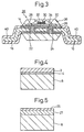
- the copper plating film 24 of the surface layer (Fig. 2) is oxidized and a copper oxide layer 25 (Fig. 5) is first formed.
- the oxygen penetrating to the lower layer oxidizes the zinc plating film 22 to form a copper oxide and zinc layer 27.
- the oxygen does not penetrate down to the copper alloy material 8 of the further lower layer, so no segregation layer 4 of the additional element as shown in Fig. 4 is formed. Due to this, the peeling of the copper oxide layer is greatly reduced.
- the oxidation of the copper alloy material 8 is suppressed, and, as a result, the peeling of the surface layer copper oxide layer is suppressed.
- Table 2 shows various under platings and results of evaluation of the plating characteristics.
- test methods used for evaluating the characteristics in Table 2 were as follows in 1) to 8):
- test pieces of the examples of the present invention are excellent in the adhesion of the oxide film, characteristics after silver plating, corrosion resistance, appearance of outer lead solder plating, and the soldering property in comparison with the test pieces of the comparative examples.
- Comparative Examples 1 and 2 it is shown that a segregation layer is formed after the heating test, and the oxide film peels off.
- Comparative Examples 4 to 6 the adhesion of the heat resistant oxide film is good, but the zinc is exposed at the surface, so the zinc leaches into the silver plating solution when applying the silver plating, the silver is precipitated on the test piece side, black patches are formed on the test piece surface, and the appearance is degraded.
- the adhesion of the silver plating film after the heating test is good in Comparative Examples 4 to 6 is considered to be the modification of the abnormally precipitated silver plating film by the heating.
- the plating solution leaks to the side wall or back side of the inner leads, so a plating film inferior in adhesion is formed at those locations. It is necessary to peel off this silver plating film.
- the silver plating peeling characteristic in the case of Comparative Examples 4 to 6, the zinc leaches into the acid peeling solution and, in the heating test after that, in the same way as Comparative Examples 1 and 2, the adhesion of the oxide film of the under plating film (copper-zinc alloy plating) is poor and the original characteristics of the copper-zinc alloy plating film are not exhibited.
- the surface is washed by an alkali to remove the resin flashes, then the under plating film is peeled off by a peeling solution containing about 10 to 15 v/v% of sulfuric acid.
- the zinc which is an amphoteric metal and has a fast reaction speed with the alkali washing solution, leaches into the alkali washing solution. For this reason, the solder plating film is abnormally precipitated in the solder plating after that, patches are formed in the heating test of the solder plating film, and the plating appearance is degraded.
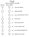
- Figure 6 shows a comparison between the conventional process of production of a lead frame and the process of production of a lead frame according to the first or second aspect of the invention.
- Figure 7 shows the process of production of a standard semiconductor device.
- Double-layer under plating films comprised of a lower layer made of a copper (50) and zinc (50) alloy and an upper layer made of copper of various thicknesses were formed on a copper alloy (Cu and 1 to 3 wt% Sn alloy) material and tested by the same test methods as in Table 2.
- the plating conditions were the same as the method explained in Embodiment 1. The results are shown all together in Table 3.
- the thickness of the copper upper layer is less than 0.02 ⁇ m, the reliability of the package, the adhesion of the under plating oxide film, the adhesion of the under plating oxide film after the silver plating, the solder plating property, and the solder bonding strength are lowered. On the other hand, if the thickness of the copper upper layer exceeds 0.4 ⁇ m, the solder bonding strength is lowered. In order to secure good levels of all of these characteristics, it is necessary to control the thickness of the copper upper layer of the under plating film to within a range of 0.02 to 0.4 ⁇ m.
- the present invention provides a semiconductor device lead frame excellent in adhesion with the sealing resin, free from contamination of the precious metal plating solution (particularly the silver plating solution), having a good appearance of the precious metal plating film, excellent in the corrosion resistance and moisture resistance, and having a good appearance and adhesion of the outer lead solder plating film, a process of production of the same, a semiconductor device using the lead frame, and a process of production of the same.
Landscapes
- Lead Frames For Integrated Circuits (AREA)
- Electroplating Methods And Accessories (AREA)
Applications Claiming Priority (5)
| Application Number | Priority Date | Filing Date | Title |
|---|---|---|---|
| JP10138099 | 1999-04-08 | ||
| JP10138099 | 1999-04-08 | ||
| JP2000013462 | 2000-01-21 | ||
| JP2000013462 | 2000-01-21 | ||
| PCT/JP2000/001836 WO2000062341A1 (en) | 1999-04-08 | 2000-03-24 | Lead frame for semiconductor device |
Publications (2)
| Publication Number | Publication Date |
|---|---|
| EP1094519A1 true EP1094519A1 (de) | 2001-04-25 |
| EP1094519A4 EP1094519A4 (de) | 2005-01-19 |
Family
ID=26442265
Family Applications (1)
| Application Number | Title | Priority Date | Filing Date |
|---|---|---|---|
| EP00911362A Withdrawn EP1094519A4 (de) | 1999-04-08 | 2000-03-24 | Leiterrahmen für halbleiteranordnung |
Country Status (6)
| Country | Link |
|---|---|
| US (1) | US6593643B1 (de) |
| EP (1) | EP1094519A4 (de) |
| KR (1) | KR100381302B1 (de) |
| CN (1) | CN1190840C (de) |
| TW (1) | TW463349B (de) |
| WO (1) | WO2000062341A1 (de) |
Cited By (1)
| Publication number | Priority date | Publication date | Assignee | Title |
|---|---|---|---|---|
| WO2004064154A1 (en) * | 2003-01-16 | 2004-07-29 | Matsushita Electric Industrial Co., Ltd. | Lead frame for a semiconductor device |
Families Citing this family (44)
| Publication number | Priority date | Publication date | Assignee | Title |
|---|---|---|---|---|
| JP2001230360A (ja) * | 2000-02-18 | 2001-08-24 | Hitachi Ltd | 半導体集積回路装置およびその製造方法 |
| DE10148120B4 (de) * | 2001-09-28 | 2007-02-01 | Infineon Technologies Ag | Elektronische Bauteile mit Halbleiterchips und ein Systemträger mit Bauteilpositionen sowie Verfahren zur Herstellung eines Systemträgers |
| US7078822B2 (en) * | 2002-06-25 | 2006-07-18 | Intel Corporation | Microelectronic device interconnects |
| US20040108580A1 (en) * | 2002-12-09 | 2004-06-10 | Advanpack Solutions Pte. Ltd. | Leadless semiconductor packaging structure with inverted flip chip and methods of manufacture |
| JP2005019922A (ja) * | 2003-06-30 | 2005-01-20 | Shinko Electric Ind Co Ltd | 半導体パッケージ用リードフレーム |
| US6966800B2 (en) * | 2004-03-22 | 2005-11-22 | Fci Americas Technology, Inc. | Overmolded electrical connector |
| KR20060030356A (ko) * | 2004-10-05 | 2006-04-10 | 삼성테크윈 주식회사 | 반도체 리이드 프레임과, 이를 포함하는 반도체 패키지와,이를 도금하는 방법 |
| US7268415B2 (en) * | 2004-11-09 | 2007-09-11 | Texas Instruments Incorporated | Semiconductor device having post-mold nickel/palladium/gold plated leads |
| US7256481B2 (en) * | 2005-11-30 | 2007-08-14 | Texas Instruments Incorporated | Leadframes for improved moisture reliability and enhanced solderability of semiconductor devices |
| DE102006001602A1 (de) * | 2006-01-11 | 2007-05-24 | Infineon Technologies Ag | Halbleiterbauteil und Verfahren zu seiner Herstellung |
| WO2008041350A1 (en) * | 2006-09-29 | 2008-04-10 | Kabushiki Kaisha Toshiba | Joint with first and second members with a joining layer located therebetween containing sn metal and another metallic material; methods for forming the same joint |
| JP5273922B2 (ja) * | 2006-12-28 | 2013-08-28 | 株式会社アライドマテリアル | 放熱部材および半導体装置 |
| US8129229B1 (en) | 2007-11-10 | 2012-03-06 | Utac Thai Limited | Method of manufacturing semiconductor package containing flip-chip arrangement |
| CN101465333B (zh) * | 2007-12-17 | 2011-04-20 | 三星电子株式会社 | 引线框架及其制造方法 |
| JP5417128B2 (ja) * | 2008-11-27 | 2014-02-12 | 新光電気工業株式会社 | リードフレーム及びその製造方法、及び半導体装置 |
| US10163766B2 (en) | 2016-11-21 | 2018-12-25 | Semiconductor Components Industries, Llc | Methods of forming leadless semiconductor packages with plated leadframes and wettable flanks |
| US10199311B2 (en) | 2009-01-29 | 2019-02-05 | Semiconductor Components Industries, Llc | Leadless semiconductor packages, leadframes therefor, and methods of making |
| US8071427B2 (en) * | 2009-01-29 | 2011-12-06 | Semiconductor Components Industries, Llc | Method for manufacturing a semiconductor component and structure therefor |
| US9899349B2 (en) * | 2009-01-29 | 2018-02-20 | Semiconductor Components Industries, Llc | Semiconductor packages and related methods |
| KR20100103015A (ko) * | 2009-03-12 | 2010-09-27 | 엘지이노텍 주식회사 | 리드 프레임 및 그 제조방법 |
| JP5573429B2 (ja) * | 2009-08-10 | 2014-08-20 | 住友ベークライト株式会社 | 無電解ニッケル−パラジウム−金めっき方法、めっき処理物、プリント配線板、インターポーザ、および半導体装置 |
| JP5634149B2 (ja) * | 2010-07-16 | 2014-12-03 | ルネサスエレクトロニクス株式会社 | 半導体装置 |
| JP2013038330A (ja) * | 2011-08-10 | 2013-02-21 | Toshiba Corp | 半導体装置の製造方法及び半導体装置 |
| EP2565297A3 (de) | 2011-08-30 | 2013-04-24 | Rohm and Haas Electronic Materials LLC | Haftungsförderung von cyanidfreier weißer Bronze |
| JP5930680B2 (ja) * | 2011-11-30 | 2016-06-08 | 株式会社日立製作所 | 半導体装置およびその製造方法 |
| JP6095997B2 (ja) * | 2013-02-13 | 2017-03-15 | エスアイアイ・セミコンダクタ株式会社 | 樹脂封止型半導体装置の製造方法 |
| JP2014192222A (ja) * | 2013-03-26 | 2014-10-06 | Shinko Electric Ind Co Ltd | リードフレーム及び半導体装置 |
| JP6044936B2 (ja) * | 2013-04-24 | 2016-12-14 | Shマテリアル株式会社 | 半導体素子搭載用基板の製造方法 |
| JP2015056540A (ja) * | 2013-09-12 | 2015-03-23 | 株式会社東芝 | 半導体装置及びその製造方法 |
| JP6284397B2 (ja) * | 2014-03-10 | 2018-02-28 | エイブリック株式会社 | 半導体装置及びその製造方法 |
| DE102014213218A1 (de) * | 2014-07-08 | 2016-02-18 | Continental Teves Ag & Co. Ohg | Sensor mit Opferanode |
| US10062639B2 (en) * | 2014-12-10 | 2018-08-28 | Stmicroelectronics Sdn Bhd | Integrated circuit device with plating on lead interconnection point and method of forming the device |
| US9070392B1 (en) | 2014-12-16 | 2015-06-30 | Hutchinson Technology Incorporated | Piezoelectric disk drive suspension motors having plated stiffeners |
| CN107735834B (zh) | 2015-06-30 | 2019-11-19 | 哈钦森技术股份有限公司 | 具有改进的可靠性的盘驱动器头部悬架结构 |
| CN106816424A (zh) * | 2015-12-01 | 2017-06-09 | 安世有限公司 | 电子元件及其制造方法、用于该电子元件的引线框架 |
| EP3427297B1 (de) * | 2016-03-11 | 2020-07-15 | ATOTECH Deutschland GmbH | Leiterrahmenstruktur, leiterrahmen, oberflächenmontierte elektronische vorrichtung und verfahren zur herstellung davon |
| JP6763607B2 (ja) * | 2017-01-12 | 2020-09-30 | 大口マテリアル株式会社 | リードフレーム及びその製造方法 |
| US10147697B1 (en) * | 2017-12-15 | 2018-12-04 | Nxp Usa, Inc. | Bond pad structure for semiconductor device packaging |
| US10892209B2 (en) | 2019-03-25 | 2021-01-12 | Texas Instruments Incorporated | Semiconductor device with metal die attach to substrate with multi-size cavity |
| US11532539B2 (en) | 2020-12-29 | 2022-12-20 | Semiconductor Components Industries, Llc | Semiconductor package with wettable flank |
| JP7580282B2 (ja) * | 2021-01-26 | 2024-11-11 | エイブリック株式会社 | 半導体装置およびその製造方法 |
| US20230096480A1 (en) * | 2021-09-28 | 2023-03-30 | Stmicroelectronics S.R.L. | Anti-whisker counter measure using a method for multiple layer plating of a lead frame |
| CN114300365B (zh) * | 2021-11-27 | 2023-01-03 | 昆山弗莱吉电子科技有限公司 | 铜合金引线框架的后处理工艺以及铜合金引线框架 |
| KR102695962B1 (ko) * | 2022-11-21 | 2024-08-20 | 해성디에스 주식회사 | 리드 프레임 및 그 리드 프레임을 포함하는 반도체 패키지 |
Family Cites Families (16)
| Publication number | Priority date | Publication date | Assignee | Title |
|---|---|---|---|---|
| JPS53141577A (en) * | 1977-05-17 | 1978-12-09 | Mitsubishi Electric Corp | Lead frame for integrated circuit |
| JPS58181888A (ja) * | 1982-04-02 | 1983-10-24 | Furukawa Electric Co Ltd:The | 銀被覆材料とその製造方法 |
| JPS60147147A (ja) * | 1984-01-10 | 1985-08-03 | Hitachi Cable Ltd | 半導体用リ−ドフレ−ム |
| JPS6341057A (ja) | 1986-08-07 | 1988-02-22 | Furukawa Electric Co Ltd:The | Ag被覆電子部品用リ−ド材 |
| JPH01212790A (ja) * | 1988-02-18 | 1989-08-25 | Kobe Steel Ltd | 半導体装置用リードフレーム |
| JPH04212443A (ja) * | 1990-11-13 | 1992-08-04 | Mitsui High Tec Inc | リードフレーム |
| JP2607319B2 (ja) | 1991-07-15 | 1997-05-07 | 松下電工株式会社 | プログラマブルコントローラ |
| JP2925815B2 (ja) * | 1991-10-29 | 1999-07-28 | 古河電気工業株式会社 | 半導体チップ実装用リードフレームとその製造方法 |
| JPH0750377A (ja) * | 1993-08-05 | 1995-02-21 | Kobe Steel Ltd | 半導体用リードフレーム |
| US5650661A (en) * | 1993-12-27 | 1997-07-22 | National Semiconductor Corporation | Protective coating combination for lead frames |
| JPH07307426A (ja) * | 1994-05-13 | 1995-11-21 | Furukawa Electric Co Ltd:The | 電子機器部品用銅系条材とその製造方法 |
| JPH09116065A (ja) * | 1995-10-17 | 1997-05-02 | Dainippon Printing Co Ltd | リードフレーム |
| JP3701373B2 (ja) * | 1995-11-17 | 2005-09-28 | 大日本印刷株式会社 | リードフレームとリードフレームの部分貴金属めっき方法、及び該リードフレームを用いた半導体装置 |
| KR100266726B1 (ko) * | 1995-09-29 | 2000-09-15 | 기타지마 요시토시 | 리드프레임과 이 리드프레임을 갖춘 반도체장치 |
| US6037653A (en) * | 1997-03-25 | 2000-03-14 | Samsung Aerospace Industries, Ltd. | Semiconductor lead frame having multi-layered plating layer including copper-nickel plating layer |
| US6203931B1 (en) * | 1999-02-05 | 2001-03-20 | Industrial Technology Research Institute | Lead frame material and process for manufacturing the same |
-
2000
- 2000-03-24 CN CNB008009260A patent/CN1190840C/zh not_active Expired - Lifetime
- 2000-03-24 KR KR10-2000-7013802A patent/KR100381302B1/ko not_active Expired - Fee Related
- 2000-03-24 US US09/719,329 patent/US6593643B1/en not_active Expired - Lifetime
- 2000-03-24 EP EP00911362A patent/EP1094519A4/de not_active Withdrawn
- 2000-03-24 WO PCT/JP2000/001836 patent/WO2000062341A1/ja not_active Ceased
- 2000-03-31 TW TW089106069A patent/TW463349B/zh not_active IP Right Cessation
Cited By (4)
| Publication number | Priority date | Publication date | Assignee | Title |
|---|---|---|---|---|
| WO2004064154A1 (en) * | 2003-01-16 | 2004-07-29 | Matsushita Electric Industrial Co., Ltd. | Lead frame for a semiconductor device |
| US7692277B2 (en) | 2003-01-16 | 2010-04-06 | Panasonic Corporation | Multilayered lead frame for a semiconductor light-emitting device |
| US7994616B2 (en) | 2003-01-16 | 2011-08-09 | Panasonic Corporation | Multilayered lead frame for a semiconductor light-emitting device |
| US8541871B2 (en) | 2003-01-16 | 2013-09-24 | Panasonic Corporation | Multilayered lead frame for a semiconductor light-emitting device |
Also Published As
| Publication number | Publication date |
|---|---|
| TW463349B (en) | 2001-11-11 |
| CN1306676A (zh) | 2001-08-01 |
| KR100381302B1 (ko) | 2003-04-26 |
| CN1190840C (zh) | 2005-02-23 |
| KR20010052602A (ko) | 2001-06-25 |
| US6593643B1 (en) | 2003-07-15 |
| WO2000062341A1 (en) | 2000-10-19 |
| EP1094519A4 (de) | 2005-01-19 |
Similar Documents
| Publication | Publication Date | Title |
|---|---|---|
| US6593643B1 (en) | Semiconductor device lead frame | |
| US6034422A (en) | Lead frame, method for partial noble plating of said lead frame and semiconductor device having said lead frame | |
| US6646330B2 (en) | Lead frame for semiconductor device, process for producing the same and semiconductor device using the same | |
| EP1480270B1 (de) | Packungsanordnung und Halbleitergehäuse | |
| JP3228789B2 (ja) | 樹脂用インサート部材の製造方法 | |
| US9177833B2 (en) | Semiconductor device and method of manufacturing the same | |
| US20030011048A1 (en) | Semiconductor circuit assembly having a plated leadframe including gold selectively covering areas to be soldered | |
| US20110079887A1 (en) | Lead frame and method of manufacturing the same | |
| US5486721A (en) | Lead frame for integrated circuits | |
| US6995042B2 (en) | Method for fabricating preplated nickel/palladium and tin leadframes | |
| JPH09148508A (ja) | 半導体装置用リードフレーム及びこれを用いた樹脂封止型半導体装置 | |
| KR101120288B1 (ko) | 성장 형성물 감소 방법 및 장치와 집적 회로 | |
| US6287896B1 (en) | Method for manufacturing lead frames and lead frame material for semiconductor device | |
| JP2925815B2 (ja) | 半導体チップ実装用リードフレームとその製造方法 | |
| JPH11121673A (ja) | リードフレーム | |
| JPH07326701A (ja) | 電気電子部品用導電材、リードフレ−ム及びそれを使用した半導体集積回路 | |
| JPH10284667A (ja) | 耐食性、耐酸化性に優れる電気電子機器用部品材料、及びその製造方法 | |
| KR100378489B1 (ko) | 은 또는 은 합금도금을 이용한 반도체 패키지용 리드프레임 및 그 제조방법 | |
| JP3402228B2 (ja) | 鉛を含まない錫ベース半田皮膜を有する半導体装置 | |
| JPH09199655A (ja) | リードフレームとリードフレームの部分貴金属めっき方法、及び該リードフレームを用いた半導体装置 | |
| JP2570911B2 (ja) | 半導体パッケージ及びそれに用いるリードフレーム | |
| JP3481448B2 (ja) | リードフレーム | |
| KR100203334B1 (ko) | 다층도금 리드프레임 | |
| KR100209264B1 (ko) | 반도체 리드 프레임 | |
| JPWO2000062341A1 (ja) | 半導体装置用リードフレーム |
Legal Events
| Date | Code | Title | Description |
|---|---|---|---|
| PUAI | Public reference made under article 153(3) epc to a published international application that has entered the european phase |
Free format text: ORIGINAL CODE: 0009012 |
|
| 17P | Request for examination filed |
Effective date: 20001211 |
|
| AK | Designated contracting states |
Kind code of ref document: A1 Designated state(s): AT BE CH CY DE DK ES FI FR GB GR IE IT LI LU MC NL PT SE |
|
| RBV | Designated contracting states (corrected) |
Designated state(s): DE FR GB |
|
| A4 | Supplementary search report drawn up and despatched |
Effective date: 20041207 |
|
| RIC1 | Information provided on ipc code assigned before grant |
Ipc: 7H 01L 23/50 A Ipc: 7H 01L 23/495 B |
|
| 17Q | First examination report despatched |
Effective date: 20080215 |
|
| STAA | Information on the status of an ep patent application or granted ep patent |
Free format text: STATUS: THE APPLICATION IS DEEMED TO BE WITHDRAWN |
|
| 18D | Application deemed to be withdrawn |
Effective date: 20080626 |