EP1137052A1 - Automatisches Kalibrationssystem für einen Scheibentransferroboter - Google Patents
Automatisches Kalibrationssystem für einen Scheibentransferroboter Download PDFInfo
- Publication number
- EP1137052A1 EP1137052A1 EP00105965A EP00105965A EP1137052A1 EP 1137052 A1 EP1137052 A1 EP 1137052A1 EP 00105965 A EP00105965 A EP 00105965A EP 00105965 A EP00105965 A EP 00105965A EP 1137052 A1 EP1137052 A1 EP 1137052A1
- Authority
- EP
- European Patent Office
- Prior art keywords
- wand
- robot
- sensor
- enclosure
- controller
- Prior art date
- Legal status (The legal status is an assumption and is not a legal conclusion. Google has not performed a legal analysis and makes no representation as to the accuracy of the status listed.)
- Granted
Links
Images




Classifications
-
- H—ELECTRICITY
- H10—SEMICONDUCTOR DEVICES; ELECTRIC SOLID-STATE DEVICES NOT OTHERWISE PROVIDED FOR
- H10P—GENERIC PROCESSES OR APPARATUS FOR THE MANUFACTURE OR TREATMENT OF DEVICES COVERED BY CLASS H10
- H10P72/00—Handling or holding of wafers, substrates or devices during manufacture or treatment thereof
- H10P72/50—Handling or holding of wafers, substrates or devices during manufacture or treatment thereof for positioning, orientation or alignment
- H10P72/53—Handling or holding of wafers, substrates or devices during manufacture or treatment thereof for positioning, orientation or alignment using optical controlling means
-
- H—ELECTRICITY
- H10—SEMICONDUCTOR DEVICES; ELECTRIC SOLID-STATE DEVICES NOT OTHERWISE PROVIDED FOR
- H10P—GENERIC PROCESSES OR APPARATUS FOR THE MANUFACTURE OR TREATMENT OF DEVICES COVERED BY CLASS H10
- H10P72/00—Handling or holding of wafers, substrates or devices during manufacture or treatment thereof
- H10P72/30—Handling or holding of wafers, substrates or devices during manufacture or treatment thereof for conveying, e.g. between different workstations
- H10P72/34—Handling or holding of wafers, substrates or devices during manufacture or treatment thereof for conveying, e.g. between different workstations the wafers being stored in a carrier, involving loading and unloading
- H10P72/3402—Mechanical parts of transfer devices
Definitions
- This invention relates to control systems for robots, and more particularly to a method and apparatus for automatically calibrating or "teaching" a robot to position itself at a plurality of pre-selected positions.
- a robotic handling system In the fabrication of semiconductors, silicon wafers are held in a cassette and then moved to various pre-programmed processing locations by a robotic handling system.
- the latter typically includes a mechanism with degrees of freedom in radial (R), angular ( ⁇ ) and vertical (Z) directions and having a robot arm with a vacuum or edge-gripping wand.
- the robot must be able to pick up wafers from a storage cassette and then transfer them to a designated station or a plurality of stations where the wafer will undergo some arbitrary process such as heating or alignment.
- the robot In order to perform these actions, the robot must have precise knowledge of the R, ⁇ and Z positions of the wafer at all cassette and station locations.
- a robot control system must provide the aforesaid knowledge to position the robot arm and thus the gripped wafer precisely within a cassette or process station for each robot function.
- the robot To provide proper operation of the robot system when initially set up or when restarted after replacement of a component or when a process location has been changed, the robot must be programmed or "taught" so that for each operation phase, the robot arm is positioned precisely at the proper location for the desired function.
- this initial and/or subsequent programming or "teaching" step was accomplished by trained personnel using visually estimated trial and error adjustments of the robot mechanism and control.
- Further objects of the invention are to provide a wafer-handling automatic calibration system that will automatically calibrate and adjust a wafer handling robot in a relatively short time, for example, after robot components have been removed and replaced.
- Another object of the invention is to provide an automatic calibration system for a wafer handling robot which utilizes a machine controller that is programmed to utilize known dimensional data as well as sensor inputs from the robot and the process stations to control robot movements to precise wafer contacting locations.
- Still another object of the invention is to provide a robotic wafer handling system having improved reproducibility of the position of the wafer holding wand in the locale where a semiconductor wafer is placed or removed from an enclosure by virtue of the known dimensional data of the wand and enclosure as well as sensor inputs from the robot and the process stations to control robot movement to precise wafer contacting locations.
- an automatic calibration system for a robotic wafer handling apparatus comprised of a robot with three degrees of freedom in the radial (R), angular ( ⁇ ), and vertical (Z) directions.
- the robot which is connected to a machine controller having a memory section and logic circuitry, has a movable robot arm which can be extended to reach a preselected location such as a cassette containing semiconductor wafers and one or more of a plurality of processing stations.
- processing station may include wafer holding boats or cassettes, or any enclosure of fixture which is adapted to retain a wafer or disc for some processing purpose.
- a wand having a wafer engaging and retaining means such as an edge grip device or a vacuum port that enables it to pick-up, place and transport wafers from and to cassettes and to process stations where the wafer will undergo some arbitrary process such as heating or alignment.
- the robot In order to perform these actions, the robot must have precise knowledge of the R, ⁇ and Z positions at which to pick-up and place wafers at both locations.
- the present invention provides a means for automatically determining or calibrating the various required robot positions with no operator intervention.
- the controller has a memory section which is supplied with initial data including nominal R, ⁇ and Z pick-up and drop off positions of the wafers at the process stations and cassettes of the system. Also, the controller memory is provided with vital dimensional characteristics of the robot and the process stations and cassettes that are serviced by the robot.
- the controller is connected to an I/O system which receives sensor signals from the robot arm, the process stations and cassettes as well as from the robot motors.
- the robot which may be of a commercially available type, consists of three motors (R, ⁇ and Z), a vacuum solenoid valve, a vacuum present sensor or edge gripping means, an R axis home switch, and preferably, a laser sensor.
- the robot's Z axis motor moves, the entire robot arm translates along the Z axis (see Figure 1).
- the ⁇ axis motor causes the entire arm to rotate about point A in an angular ⁇ direction.
- the R axis motor causes the arm to extend radially out along the R axis such that the wand is still along the centerline of the robot through a point A, but further or closer to point A.
- the machine controller is programmed to move each of the motors to a commanded position and to process the I/O data.
- encoders provide feedback signals to the controller to indicate the current position of the motor.
- the encoder data is stored in the memory of the controller at regular intervals.
- a feedback loop within the controller Based on the actual motor feedback position and the desired motor position (i.e., the commanded motor position), which is determined by the software in the controller, a feedback loop within the controller produces the voltage outputs required to move the motors to their desired positions. These voltage outputs are sent to the motors via the amplifier. Since the motors are actually run by changing the current to the motor, an amplifier in the controller converts the voltage output to the appropriate current output.
- the controller collects I/O data from the I/O system.
- the controller stores digital input point states (i.e. On or Off signals) from the I/O system in its own memory and sends digital output states from its memory to the I/O system.
- the I/O system collects the input point states of each of the input devices (e.g., a vacuum present sensor) and sends the output point states to the appropriate output devices (e.g. vacuum solenoid valve).
- the I/O system coordinates the signal paths so that the device states go to the correct memory locations in the controller.
- the first is a twin beam laser sensor attached to the back of the wand on the robot arm which provides a digital output depending on whether the emitted laser is reflected back from an object and sensed at the receiver.
- a twin beam laser sensor attached to the back of the wand on the robot arm which provides a digital output depending on whether the emitted laser is reflected back from an object and sensed at the receiver.
- the second type of sensor is a thrubeam sensor which is used on the process station. Like the laser sensor on the robot, this sensor has a sender/receiver component pair which are aligned vertically at a process station and provide a digital output depending on whether the receiver senses the infrared LED signal from the sender. Thus, this sensor detects when an object such as the robot wand is moved horizontally between the sender/receiver beam.
- the third sensor type is a reflective LED sensor which is similar to the thrubeam sensor except that its sender and receiver are contained in the same unit (see Figure 8). This sensor can determine when an object is placed in front of it by detecting the reflected light signal. Such a sensor is provided on the cassette to determine the final R value of the robot for contacting a wafer in the cassette.
- a typical autocalibration procedure for a process station is accomplished broadly, as follows: With the controller properly programmed, including designation of nominal R, ⁇ and Z positions of all stations and cassettes, the operator must only press a "Start" button. The controller first commands the robot to move into a position where the robot sensor laser can perform a rough Z-direction scan of the vertical reference plane on the process station. Thus, the robot is moved to an initial or nominal calibration position based on Rnom, ⁇ nom, and Znom. The wand is first rotated to its reverse ⁇ position so that its sensor faces the targeted process station. The robot with the wand is moved in a negative Z position until the laser is turned on to define a Z rough position.
- the controller then commands the robot to establish the ⁇ calibration using the vertically oriented sensor located at the process station or cassette.
- the robot is moved to an initial calibration position based on Rnom, ⁇ nom and Zrough.
- the robot is moved in a positive ⁇ direction until the sensor is turned on and records a ⁇ position.
- the robot is then moved in a negative ⁇ direction until another sensor is turned on to indicate a second ⁇ 2 position.
- the ⁇ 1 and ⁇ 2 positions represent opposite side edges of the wand.
- the calibrated ⁇ cal position is now calculated by dividing ⁇ , and ⁇ 2 values by 2.
- the controller now commands the robot to proceed with the R calibration by moving it to an initial calibration position based on R nom ⁇ cal and Z rough .
- the robot arm is moved in the R direction until the process station sensor is activated to define the measured R position.
- the final Z calibration is accomplished as the controller moves the robot to an initial calibration position based on Rcal, ⁇ cal, and Z rough .
- the robot is again moved in the negative Z direction with the wand reversed and its sensor facing the vertical plane of the process stations or cassette opening at its optimum scanning distance. As the edge of the opening is encountered, the wand sensor is triggered to define the measured Z position.
- the controller can be programmed to accommodate a large number of cassettes or process stations that are within the reach or scope of the connected robot. For each stations or cassette a precise movement of the robot arm can be controlled so that contact, support and transport of the targeted semiconductor wafer can be accomplished with reliability and maximum efficiency.
- the laser sensor on the rotatable wand of the robot is also used for mapping a cassette to provide an indication of the presence of wafers in the cassette.
- a robot without the wand sensor may be used in a modified form of the invention.
- an additional horizontal beam sensor is provided in the opening of each process station to enable the Z position of the robot to be calibrated.
- Fig. 1 is a diagrammatic view of a wafer handling robot system that provides autocalibration in accordance with the principles of the present invention.
- Fig. 2 is a fragmentary view in perspective of the robot for the system of Fig. 1.
- Fig. 2A is a plan view of the wafer contacting wand for the robot of Fig. 2.
- Fig. 2B is a side view in elevation of the robot wand of Fig. 2.
- Fig. 3 is a fragmentary view in perspective of the robot of Fig. 2 and a process station as it appears with its wand in reverse position during a preliminary sensing step before entering the process station.
- Fig. 3A is a plan view of a typical process station as shown in Fig. 3.
- Fig. 3B is a side view in elevation of the process station of Fig. 3A.
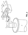
- Fig. 4 is a view in perspective similar to Fig. 3 and showing the robot wand extending partially within the process station.
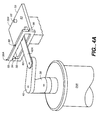
- Fig. 4A is a view in perspective showing an alternate form of the invention with a modified sensor arrangement.
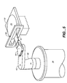
- Fig. 5 is a view in perspective similar to Fig. 4 showing the robot wand fully within the process station and in contact with a wafer therein.
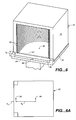
- Fig. 6 is a view in perspective of a typical cassette holder for semiconductor wafers.
- Fig. 6A is a slightly reduced horizontal plan view of the cassette holder of Fig. 6.
- Fig. 7 is a view in perspective showing the robot of Fig. 2 as it appears extended with its wand in contact with a wafer within the cassette holder of Fig. 6.
- Fig. 8 is an enlarged view in perspective of the sensor that is mounted on the robot wand.
- Fig. 9 is an enlarged exploded view of the transmitter and receiver elements of a thrubeam sensor that is used on the process station.
- Fig. 10 is an enlarged view in perspective of a sensor used on the cassette shown in Fig. 6.
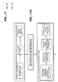
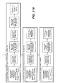
- Figs. 11A and 11B constitute a flow chart showing the functional steps for accomplishing the autocalibration of the robot shown in Fig. 1, according to the invention.
- Fig. 1 shows diagrammatically a semiconductor wafer handling apparatus 20 including a robot 22 that utilizes an autocalibration system embodying principles of the present invention.
- the robot is electrically connected to a machine controller 24, a motor amplifier 26 and an I/O component 28.
- the robot is automatically controlled to locate and move to precise locations which enable it to remove or replace wafers from one or more storage devices such as a boat or cassette stand 30 and to and from one or more process stations 32.
- electrical connections from a cassette and from a process station furnish sensor signals to the I/O component 28.
- the semiconductor wafers referred to above and identified by numeral 25 in the drawing may be any form of semiconductor wafer having a uniform thickness and diameter.
- the robot 22 has three degrees of movement in the radial (R), angular or theta ( ⁇ ) and vertical directions.
- it comprises a base support 34 from which is cantilevered an articulated robot arm 36.
- the latter is comprised of a first robot arm section 38 to the end of which is a second pivotally connected outer arm section 40 .
- Pivotally attached to the outer arm section 40 is a wand 42 whose outer end is generally Y-shaped with spaced apart fingers 43.
- Vacuum ports (not shown) are provided on the wand which enable it to retain a wafer in order to pick up and transport the wafer from a cassette to a process stations and vice-versa.
- the robot 22 is of a type that is commercially available and also has a vacuum solenoid valve, a vacuum present sensor, and an R axis home switch. As the robot's Z axis motor moves, the entire robot arm 36 translates vertically along the Z axis. The theta axis motor causes the arm 36 to move angularly about the Z axis and the R motor causes the wand 42 to move along the R axis that extends radially from a point A at the centerline of the robot.
- FIG. 2 A more detailed view of the robot 22 and its wand 42 is shown in Fig. 2.
- the point A which is on the Z axis of the robot and a point B which is on the pivotal axis of the second arm 40 and the wand 42, establish the R axis.
- Mounted on the rear end of the wand by a retainer 45 is a laser sensor 44 which is preferably of the twin beam reflective type.
- the embodiment shown (See Fig. 8) has two spaced apart laser emitters 46 and two laser sensor receiver elements 48 and it provides a digital output whenever a reflected laser is sensed at a receiver element.
- this laser 44 will only produce an output signal if there is an object in front of the sensor which can reflect the laser back to the sensor.
- This laser sensor has an optimum scanning distance d 11 (see Fig. 8) with a limited range of operation.
- the point B is located on a longitudinal centerline 50 of the wand. Also on this centerline is point C on the outer edge of the sensor 44, point D which is on the wand edge between the wand fingers 43 and point E which is the optimum wafer pick-up center, also between the wand fingers. As shown, the distances between points C and E are important dimensions in the autocalibration procedure and are stored in the memory of the controller 24.
- points F and G which are utilized in the theta position measurements.
- the laser/wand offset (LW OFF ) or d 13 is the distance between the top wafer-contacting plane 52 of the wand and the plane 54 of the laser emitters in the sensor 44.
- the top wafer plane 52 is coplanar with the upper edge of the beam from the laser emitters.
- wand 42 is shown, pivotally mounted at the end of the outer arm 40 and in its reversed 180° position .
- the sensor 44 can face a process station 32 as it commences its scanning procedure which will be described below.
- the process station as shown, is representative of various types and forms used for different semiconductor processing steps and generally has a frame 56 forming a frontal opening 58 whose outer surface 60 is in a vertical reference plane 61.
- the frame 56 has a top outer edge 62, and top and bottom inner edges 64 and 66 of the opening 58.
- the distance d 5 between edges 62 and 64 and the distance d 6 between edges 64 and 64 are also stored in the memory of the controller.
- Attached to the base member 59 are three spaced apart wafer-supporting pins 65 of equal height which positioned to retain a wafer above the surface 63 while it is being processed.
- the frame is fixed to a horizontal base member 59 having a horizontally planar upper surface 63.
- the process station 32 is provided with a laser sensor 68 which is mounted in the frame 56 the surrounds the opening 58.
- This sensor is thrubeam type sensor, of the type shown in Fig. 9 and comprises an emitter element 70 in the upper frame portion which transmits a laser beam to a vertically aligned receiver element 72 in the lower frame portion. When the beam between these two elements is blocked, a sensor signal is generated.
- a centerpoint 74 of the process station 32, as shown in Fig. 3A denotes the desired center of the wafer which is placed within the process station.
- the distance from centerpoint 74 to the sensor elements 70 and 72 is designated as d 9 .
- a shorter distance designated as d 10 extends from the sensor 68 to the outer surface or reference plane 61 of the process station 32.
- the values for d 9 and d 10 are also stored in the controller memory.
- the desired pick up height of the wafer is a distance d 7 above the horizontal plane of the process station base member 59 provided by the pins 65.
- This d 7 value is also stored in the computer memory and is used later in determining the final Z position for the wand 42.
- a typical wafer holding cassette 30 is shown in Fig. 6 and comprises essentially a housing 78 with an open front and a series of curved interior grooves 80 forming slots between them for retaining circular wafers.
- the housing is attached to a base 82 with a frontal member 84 that supports a sensor 86 which is located at a midpoint of the frontal member 84.
- the sensor 86 is preferably of the reflective LED type, as shown in Fig. 10. This sensor operates like the thrubeam sensor except that sender and receiver elements 88 and 90 are contained in the same unit and in use they can determine when an object is placed in front of them by detecting the reflected light signal. As with the other sensors, the sensor 86 provides signals to the I/O unit 28 which is connected to the controller 24.
- the sensor is flush with the upper surface 85 of the frontal element and is directed vertically upward. As indicated in Fig. 6, a distance d 4 extends above the upper surface 85 of the frontal member 84 and the sensor 86 to the plane of a wafer, shown as dotted line 92, that may be placed in the lowermost slot 80 of the cassette 30.
- the distance d 4 as well as the spacing of the slots above the sensor are stored in the controller memory.
- the sensor 86 in the frontal element 84 is spaced inwardly from its outer edge by a distance d 12 .
- the distance from sensor 86 to the nominal centerline 94 of the wafers to be stored in the cassette 30 is designated as d 8 .
- These distances d 8 and d 12 are also stored in the controller memory as previously described for other dimensions.
- each of the robot motors is moved to a limit to define the zero position of the motor.
- This procedure is predefined by the software in the controller.
- the Z axis is commanded by the controller to move in the negative direction until a mechanical hard limit is reached.
- the position where the limit is detected i.e., the motor will no longer move in the negative direction
- the controller On the R axis, the R axis home switch is used to define the limit.
- This home switch is located mechanically within the robot so that when the R axis motor passes a specific mechanical location, the state of the R axis home switch changes from 'on' to 'off' (this signal is sent to the controller 24 via the I/O system 28).
- the controller moves the R axis until the home switch state change is detected.
- the controller captures the position and defines the position as some predefined offset relative to zero.
- Zero on the R axis is defined to be the position where the distance from A to B is zero (see Figure 2).
- the theta axis zero position is defined relative to a mechanical hard limit in the same way as the Z axis.
- the operator can initiate the autocalibration procedure.
- the software to execute this procedure is again already contained in the controller 24.
- the operator must only press a 'Start' button.
- the procedures for calibrating the R, ⁇ and Z positions of the wafer at the cassette 30 and the process station 32 are similar with the exception of the sensors used.
- the precise type of sensor is not critical, only that it be able to detect when an object is placed in front of it.
- nominal or rough R, ⁇ and Z approximation pick-up and drop-off positions of wafers at process stations and cassettes must be known. These values will already be contained in the memory of the controller. A relatively loose tolerance (e.g. plus or minus 0.5 inches) is allowed for these nominal values.
- the autocalibration procedure for the process station 32 is described first.
- the initial R position (R init ) for the wand during the rough-Z scan is calculated by the controller 24 based on the known geometry of the station 32, the robot wand dimensions, and the nominal R position (R nom ).
- the initial R position (R init ) is related to the nominal R (R nom ) position by the following equation using the dimensions shown in Figs. 2A and 3A.
- R init -(R nom +d 2 +d 3 -d 9 -d 10 ) - (d 1 +d 11 )
- R nom is roughly the position where point E (Fig. 2A) of the wand will coincide with the center position 74 (Fig. 3A) of the wafer at the station 32 (assuming the nominal theta ( ⁇ ) position is used).
- R nom +d2+d 3 is therefore the position where point B is at the same position.
- R nom +d 2 +d 3 -d 9 -d 10 is then the position where B lies over the edge of the reference plane. If this term is negated, point B is again over the edge of the reference plane when the angle theta is offset by 180° relative to the nominal theta, as mentioned above.
- d 1 +d 11 the optimum scanning distance, Fig. 8 puts the point C on the laser at approximately the optimal scanning distance from the reference plane 61, subject to errors in the nominal position.
- the nominal Z is the approximate pickup position of a wafer within the process station 32, so adding the distances d 6 and d 5 (Fig. 3) along with some small error term places the robot safely above the frame 56 of the process station.
- This rough Z calibration safely defines the Z position where the wand 42 can be placed into the slot opening 58 for the R and ⁇ calibration described below.
- the controller commands the robot 34 to move to the rough Z calibration position and to the nominal R and ⁇ positions so the wand will be within the process station opening 58 (see Figure 4).
- the vertical thrubeam sensor 68 is at a known radial distance ( d9 ) from the desired center position 74 of a wafer to be placed in the station and is at the same ⁇ position as the desired center of the wafer.
- the controller 24 then commands the robot wand 42 to move in the positive ⁇ direction until the controller 24 reads that the sensor state has turned 'on' and the wand is clear of the sensor 68.
- the controller immediately records this ⁇ position ( ⁇ 1 ) as the position of point F in Fig. 2A and stops the robot.
- the robot is then commanded to move in the negative ⁇ direction until the controller 24 reads that the sensor 68 first turns 'off,' meaning the wand 42 is again in the sensor beam, and then turns 'on,' meaning the wand has cleared the sensor beam on the other side of the wand at point G.
- the controller again stores the new ⁇ position ( ⁇ 2 ) at the sensor 'on' location as the position of point G (Fig. 2A).
- the R position can now be calibrated.
- the controller 24 commands the robot 34 to move the wand 42 to the ⁇ cal position so that the vertical sensor 68 is again blocked and located along the centerline of the wand.
- the controller retracts the robot R axis until the sensor 68 turns on and the wand is again clear of the sensor.
- the controller stops the axis and captures the R position (R meas ) when the sensor state change occurs as the position of point D (Fig. 2A).
- the final measurement at the process station uses the robot laser to perform the final Z calibration.
- the controller 24 commands the robot 34 to move such that the laser sensor 44 is again facing the vertical reference plane, as shown in Fig. 3, although now the calibrated position for R and ⁇ are used in the calculations.
- the rough calibration position is used so that the laser sensor 44 is facing within the slot opening 58.
- the sensor face is now positioned by the controller to be exactly at the optimum scanning distance from the reference plane 61 at the face of the process station 32 since the R position has been calibrated.
- the controller moves the robot down in the Z direction until the lower edge 65 of the slot 58 is detected by the wand sensor.
- the Z position (Z meas ) at which the laser detects the lower edge 66 is captured by the controller.
- the vertical reference plane formed by the outer surface of the frontal member 84 is used in calibrating the robot for the cassette 30 which is mounted on a suitable cassette stand (see Figure 6).
- the initial scan of the sensor 44 in the Z-direction roughly measures the Z position of the upper edge 85 of this plane.
- the starting locations for this scan (R init , ⁇ init and Z init ) are based on the geometrical parameters, the nominal R, ⁇ and Z positions (R nom , ⁇ nom and Z nom ,) of the lowest wafer, and some safe error term to ensure that the sensor 44 is originally positioned and starts out above the reference surface 85.
- ⁇ init ⁇ nom +180
- R init -(R nom +d 2 +d 3 -d 8 -d 12 ) - (d 1 +d 11 )
- Z init Z nom' 1+(error term)
- the R and ⁇ positions of all the wafers in the cassette are the same, and the Z positions are multiples of the wafer spacing from the lowest wafer.
- the robot can be readily programmed to remove or place wafers in any or all of the cassette slots 80, as shown in Fig. 7.
- a flow chart is provided which sets forth the sequential steps for the automatic calibration system according to the present invention.
- the machine controller 24 may be readily programmed to accomplish the aforesaid steps.
- the controller itself may be of any suitable type such as shown in U.S. Patent Nos. 4,639,884 and 5.062,064.
- the robot 34 is provided with sensor 44 on its wand 42 to provide a means for determining the Z position at each processing station 32 in the manner described. If a mapping function for the robot is not required, a modified and less expensive robot can be utilized which can be the same as robot 34 but does not have a sensor 44 on its wand segment.
- a secondary embodiment a robot 34A is shown which is utilized in conjunction with a processing station 32A having a horizontal thrubeam type laser sensor 69 that is mounted in a frame 56A that surrounds the process station opening 58A.
- This sensor 69 comprises an emitter element 94 which transmits a beam horizontally across the opening 58A to an aligned receiver element 96. When the beam between these two elements is blocked, a sensor signal is generated and furnished to the controller 24.
- the horizontal thrubeam sensor 69 is provided with its elements at opposite ends of the rectangular opening 58A.
- the horizontal sensor 69 enables the robot 34A to determine the precise Z position in the following manner, with this alternate method, a rough Z position calibration is not required because the nominal Z position stored in the controller memory is made sufficiently accurate to perform the ⁇ and R calibrations.
- the horizontal sensor 69 is now used for the final Z calibration. After the R and ⁇ calibrations have been accomplished, while the robot wand is still within the slot opening of the process station, the controller commands the robot 34A to move in the vertical direction until the horizontal sensor beam across the opening of the process station is touched. The position of the wand as this occurs is combined with the known vertical offset between the sensor beam and the desired Z calibration position.
- the sequence of operations for this alternate method comprises: (1) performing the ⁇ calibration using the vertical thrubeam sensor 69; performing the R calibrations using the same vertical thrubeam sensor 68 as step 2; and making the final Z calibration using the horizontal thrubeam 69.
- the precise positioning data is stored in the controller memory and the robot wand 42A continues to remove or place a wafer within the process station as programmed.
Landscapes
- Manipulator (AREA)
- Container, Conveyance, Adherence, Positioning, Of Wafer (AREA)
Priority Applications (6)
| Application Number | Priority Date | Filing Date | Title |
|---|---|---|---|
| US09/270,261 US6075334A (en) | 1999-03-15 | 1999-03-15 | Automatic calibration system for wafer transfer robot |
| EP00105965A EP1137052B1 (de) | 1999-03-15 | 2000-03-24 | Automatisches Kalibrationssystem für einen Wafertransferroboter |
| DE2000638727 DE60038727T2 (de) | 2000-03-24 | 2000-03-24 | Automatisches Kalibrationssystem für einen Wafertransferroboter |
| AT00105965T ATE393962T1 (de) | 1999-03-15 | 2000-03-24 | Automatisches kalibrationssystem für einen wafertransferroboter |
| CA002302794A CA2302794C (en) | 1999-03-15 | 2000-03-28 | Automatic calibration system for wafer transfer robot |
| JP2000108883A JP4722251B2 (ja) | 1999-03-15 | 2000-04-11 | ウエハ移送ロボットの自動較正装置及び自動較正方法 |
Applications Claiming Priority (4)
| Application Number | Priority Date | Filing Date | Title |
|---|---|---|---|
| US09/270,261 US6075334A (en) | 1999-03-15 | 1999-03-15 | Automatic calibration system for wafer transfer robot |
| EP00105965A EP1137052B1 (de) | 1999-03-15 | 2000-03-24 | Automatisches Kalibrationssystem für einen Wafertransferroboter |
| CA002302794A CA2302794C (en) | 1999-03-15 | 2000-03-28 | Automatic calibration system for wafer transfer robot |
| JP2000108883A JP4722251B2 (ja) | 1999-03-15 | 2000-04-11 | ウエハ移送ロボットの自動較正装置及び自動較正方法 |
Publications (2)
| Publication Number | Publication Date |
|---|---|
| EP1137052A1 true EP1137052A1 (de) | 2001-09-26 |
| EP1137052B1 EP1137052B1 (de) | 2008-04-30 |
Family
ID=27427591
Family Applications (1)
| Application Number | Title | Priority Date | Filing Date |
|---|---|---|---|
| EP00105965A Expired - Lifetime EP1137052B1 (de) | 1999-03-15 | 2000-03-24 | Automatisches Kalibrationssystem für einen Wafertransferroboter |
Country Status (5)
| Country | Link |
|---|---|
| US (1) | US6075334A (de) |
| EP (1) | EP1137052B1 (de) |
| JP (1) | JP4722251B2 (de) |
| AT (1) | ATE393962T1 (de) |
| CA (1) | CA2302794C (de) |
Cited By (4)
| Publication number | Priority date | Publication date | Assignee | Title |
|---|---|---|---|---|
| US6822413B2 (en) | 2002-03-20 | 2004-11-23 | Fsi International, Inc. | Systems and methods incorporating an end effector with a rotatable and/or pivotable body and/or an optical sensor having a light path that extends along a length of the end effector |
| CN102581745A (zh) * | 2012-02-29 | 2012-07-18 | 清华大学 | 一种化学机械抛光传输机器人系统 |
| WO2012175473A3 (en) * | 2011-06-20 | 2013-04-11 | Semilev Gmbh | Method for calibrating a robot mounted on active magnetic bearings |
| EP2324968A4 (de) * | 2008-07-10 | 2015-02-25 | Kawasaki Heavy Ind Ltd | Roboter und sein lehrverfahren |
Families Citing this family (45)
| Publication number | Priority date | Publication date | Assignee | Title |
|---|---|---|---|---|
| DE19845504A1 (de) * | 1998-10-02 | 2000-04-20 | Wacker Siltronic Halbleitermat | Hordenaufnahmevorrichtung |
| US6405101B1 (en) * | 1998-11-17 | 2002-06-11 | Novellus Systems, Inc. | Wafer centering system and method |
| US6304051B1 (en) * | 1999-03-15 | 2001-10-16 | Berkeley Process Control, Inc. | Self teaching robotic carrier handling system |
| JP3458768B2 (ja) * | 1999-06-10 | 2003-10-20 | 株式会社デンソー | 負荷駆動装置 |
| US6463782B1 (en) * | 2000-01-13 | 2002-10-15 | Taiwan Semiconductor Manufacturing Co., Ltd. | Self-centering calibration tool and method of calibrating |
| US6438448B1 (en) * | 2000-02-08 | 2002-08-20 | Storage Technology Corporation | Self aligning robotic arm calibration apparatus |
| US6553280B2 (en) | 2000-07-07 | 2003-04-22 | Applied Materials, Inc. | Valve/sensor assemblies |
| US6578893B2 (en) | 2000-10-02 | 2003-06-17 | Ajs Automation, Inc. | Apparatus and methods for handling semiconductor wafers |
| US7054713B2 (en) * | 2002-01-07 | 2006-05-30 | Taiwan Semiconductor Manufacturing Company, Ltd. | Calibration cassette pod for robot teaching and method of using |
| US6567725B1 (en) | 2002-07-15 | 2003-05-20 | Speedfam-Ipec Corporation | Method and apparatus for teaching robot station location |
| US20040060186A1 (en) * | 2002-09-30 | 2004-04-01 | August Technology Corp. | Laser alignment tool |
| US6996456B2 (en) * | 2002-10-21 | 2006-02-07 | Fsi International, Inc. | Robot with tactile sensor device |
| US6852644B2 (en) * | 2002-11-25 | 2005-02-08 | The Boc Group, Inc. | Atmospheric robot handling equipment |
| US20050012938A1 (en) * | 2003-07-18 | 2005-01-20 | Jun-Ming Chen | Apparatus and method for detecting wafer position |
| US20050228542A1 (en) * | 2003-10-01 | 2005-10-13 | Varian Semiconductor Equipment Associates, Inc. | Auto-calibration method and device for wafer handler robots |
| US7230702B2 (en) * | 2003-11-13 | 2007-06-12 | Applied Materials, Inc. | Monitoring of smart pin transition timing |
| US8000837B2 (en) | 2004-10-05 | 2011-08-16 | J&L Group International, Llc | Programmable load forming system, components thereof, and methods of use |
| US20070001638A1 (en) * | 2005-07-01 | 2007-01-04 | Fsi International, Inc. | Robot with vibration sensor device |
| WO2007047163A2 (en) * | 2005-10-04 | 2007-04-26 | Applied Materials, Inc. | Methods and apparatus for drying a substrate |
| US7933685B1 (en) * | 2006-01-10 | 2011-04-26 | National Semiconductor Corporation | System and method for calibrating a wafer handling robot and a wafer cassette |
| CN101190525A (zh) * | 2006-11-22 | 2008-06-04 | 富士迈半导体精密工业(上海)有限公司 | 自动校正机械手臂 |
| JP2009049250A (ja) * | 2007-08-22 | 2009-03-05 | Yaskawa Electric Corp | ティーチング用機構を備えたカセットステージ及びそれを備えた基板搬送装置、半導体製造装置 |
| NL1036673A1 (nl) * | 2008-04-09 | 2009-10-12 | Asml Holding Nv | Robot Position Calibration Tool (RPCT). |
| US8185242B2 (en) * | 2008-05-07 | 2012-05-22 | Lam Research Corporation | Dynamic alignment of wafers using compensation values obtained through a series of wafer movements |
| US8242730B2 (en) * | 2008-06-10 | 2012-08-14 | Nichols Michael J | Automated robot teach tool and method of use |
| US8459922B2 (en) * | 2009-11-13 | 2013-06-11 | Brooks Automation, Inc. | Manipulator auto-teach and position correction system |
| US8692503B2 (en) * | 2009-12-18 | 2014-04-08 | Varian Medical Systems, Inc. | Homing and establishing reference frames for motion axes in radiation systems |
| US20130173039A1 (en) * | 2012-01-04 | 2013-07-04 | Seagate Technology Llc | Methods and devices for determining a teaching point location using pressure measurements |
| JP5532110B2 (ja) * | 2012-11-16 | 2014-06-25 | 株式会社安川電機 | 基板搬送ロボットおよび基板搬送方法 |
| TWI623994B (zh) | 2013-07-08 | 2018-05-11 | 布魯克斯自動機械公司 | 具有即時基板定心的處理裝置 |
| US9666465B2 (en) * | 2013-12-12 | 2017-05-30 | Seagate Technology Llc | Positioning apparatus |
| US10002781B2 (en) | 2014-11-10 | 2018-06-19 | Brooks Automation, Inc. | Tool auto-teach method and apparatus |
| JP2016143787A (ja) * | 2015-02-03 | 2016-08-08 | 川崎重工業株式会社 | 基板搬送ロボットおよび基板搬送方法 |
| US20160346923A1 (en) * | 2015-05-29 | 2016-12-01 | Boris Kesil | Robotic station with self-teaching functions |
| JP6965378B2 (ja) * | 2016-06-13 | 2021-11-10 | 東京エレクトロン株式会社 | 基板搬送装置および基板搬送装置の異常検出方法 |
| CN113874173B (zh) | 2019-02-08 | 2025-02-14 | 安川美国有限公司 | 对射式自动示教 |
| US11469123B2 (en) | 2019-08-19 | 2022-10-11 | Applied Materials, Inc. | Mapping of a replacement parts storage container |
| JP7413062B2 (ja) * | 2020-02-13 | 2024-01-15 | 東京エレクトロン株式会社 | 搬送装置の教示方法及び処理システム |
| US12330289B2 (en) * | 2020-08-26 | 2025-06-17 | WaferPath, Inc. | Determining the center position of a semiconductor wafer |
| US11911915B2 (en) * | 2021-06-09 | 2024-02-27 | Intrinsic Innovation Llc | Determining robotic calibration processes |
| CN113394149B (zh) * | 2021-06-30 | 2024-08-13 | 乐孜芯创自动化设备(上海)有限公司 | 具备位置检测功能的硅片传输片叉、机械手及传输方法 |
| KR102622984B1 (ko) * | 2021-08-25 | 2024-01-10 | 세메스 주식회사 | 기판 처리 장치 및 기판 처리 방법 |
| KR20240008588A (ko) * | 2022-07-12 | 2024-01-19 | 삼성전자주식회사 | 자동 티칭이 가능한 웨이퍼 이송 장치 및 이를 포함하는 반도체 공정 시스템 |
| JP2024078532A (ja) * | 2022-11-30 | 2024-06-11 | 株式会社安川電機 | 基板搬送ロボットシステムおよび基板搬送ロボットの教示方法 |
| US20250214245A1 (en) * | 2023-12-27 | 2025-07-03 | Kawasaki Jukogyo Kabushiki Kaisha | Substrate transfer apparatus and method of calibrating substrate transfer apparatus |
Citations (5)
| Publication number | Priority date | Publication date | Assignee | Title |
|---|---|---|---|---|
| US5225691A (en) * | 1992-05-18 | 1993-07-06 | Avalon Engineering, Inc. | Semiconductor wafer cassette mapper with emitter and detector arrays for slot interrogation |
| US5535306A (en) * | 1993-01-28 | 1996-07-09 | Applied Materials Inc. | Self-calibration system for robot mechanisms |
| US5651823A (en) * | 1993-07-16 | 1997-07-29 | Semiconductor Systems, Inc. | Clustered photolithography system |
| US5870488A (en) * | 1996-05-07 | 1999-02-09 | Fortrend Engineering Corporation | Method and apparatus for prealigning wafers in a wafer sorting system |
| WO2000022589A1 (en) * | 1998-10-15 | 2000-04-20 | Asyst Technologies, Inc. | Wafer mapping system |
Family Cites Families (52)
| Publication number | Priority date | Publication date | Assignee | Title |
|---|---|---|---|---|
| US3972424A (en) * | 1973-03-12 | 1976-08-03 | The Computervision Corporation | Automatic wafer loading and pre-alignment system |
| US3986109A (en) * | 1975-01-29 | 1976-10-12 | Ade Corporation | Self-calibrating dimension gauge |
| US4158171A (en) * | 1977-09-14 | 1979-06-12 | Ade Corporation | Wafer edge detection system |
| US4692695A (en) * | 1982-05-18 | 1987-09-08 | Ade Corporation | Conductivity-type sensor |
| US4646009A (en) * | 1982-05-18 | 1987-02-24 | Ade Corporation | Contacts for conductivity-type sensors |
| US4860229A (en) * | 1984-01-20 | 1989-08-22 | Ade Corporation | Wafer flatness station |
| JPS6372138A (ja) * | 1986-09-12 | 1988-04-01 | Metsukusu:Kk | シリコンウエハ−の位置決め装置 |
| US4775281A (en) * | 1986-12-02 | 1988-10-04 | Teradyne, Inc. | Apparatus and method for loading and unloading wafers |
| US4846626A (en) * | 1987-02-09 | 1989-07-11 | The Perkin-Elmer Corporation | Wafer handling system |
| US4819167A (en) * | 1987-04-20 | 1989-04-04 | Applied Materials, Inc. | System and method for detecting the center of an integrated circuit wafer |
| US4895486A (en) * | 1987-05-15 | 1990-01-23 | Roboptek, Inc. | Wafer monitoring device |
| US4897015A (en) * | 1987-05-15 | 1990-01-30 | Ade Corporation | Rotary to linear motion robot arm |
| US4880348A (en) * | 1987-05-15 | 1989-11-14 | Roboptek, Inc. | Wafer centration device |
| US5102291A (en) * | 1987-05-21 | 1992-04-07 | Hine Design Inc. | Method for transporting silicon wafers |
| US4892455A (en) * | 1987-05-21 | 1990-01-09 | Hine Derek L | Wafer alignment and transport mechanism |
| US4910453A (en) * | 1987-10-15 | 1990-03-20 | Ade Corporation | Multi-probe grouping system with nonlinear error correction |
| JPH0620097B2 (ja) * | 1987-10-20 | 1994-03-16 | 富士通株式会社 | ウエハ位置決め装置 |
| US5030057A (en) * | 1987-11-06 | 1991-07-09 | Tel Sagami Limited | Semiconductor wafer transferring method and apparatus and boat for thermal treatment of a semiconductor wafer |
| US4881863A (en) * | 1987-12-17 | 1989-11-21 | Primary Systems Corporation | Apparatus for inspecting wafers |
| US4931962A (en) * | 1988-05-13 | 1990-06-05 | Ade Corporation | Fixture and nonrepeatable error compensation system |
| US5102280A (en) * | 1989-03-07 | 1992-04-07 | Ade Corporation | Robot prealigner |
| US4958129A (en) * | 1989-03-07 | 1990-09-18 | Ade Corporation | Prealigner probe |
| US5261776A (en) * | 1989-04-27 | 1993-11-16 | Micron Technology, Inc. | Vacuum operated wafer transfer apparatus |
| JPH0736417B2 (ja) * | 1989-10-24 | 1995-04-19 | 株式会社メツクス | ウエハーの位置決め装置 |
| US4980971A (en) * | 1989-12-14 | 1991-01-01 | At&T Bell Laboratories | Method and apparatus for chip placement |
| US5265170A (en) * | 1990-01-11 | 1993-11-23 | Hine Design, Inc. | Devices and methods for reading identification marks on semiconductor wafers |
| US5135349A (en) * | 1990-05-17 | 1992-08-04 | Cybeq Systems, Inc. | Robotic handling system |
| JPH081922B2 (ja) * | 1991-01-25 | 1996-01-10 | 株式会社東芝 | ウェハ−保持装置 |
| JP2986121B2 (ja) * | 1991-03-26 | 1999-12-06 | 東京エレクトロン株式会社 | ロードロック装置及び真空処理装置 |
| JPH04298060A (ja) * | 1991-03-26 | 1992-10-21 | Tokyo Electron Ltd | ウエハの位置合わせ装置 |
| US5193969A (en) * | 1991-05-20 | 1993-03-16 | Fortrend Engineering Corporation | Wafer transfer machine |
| JPH05114641A (ja) * | 1991-10-22 | 1993-05-07 | Nippon Steel Corp | 半導体ウエハカセツトキヤリア |
| JP3410118B2 (ja) * | 1992-04-14 | 2003-05-26 | アネルバ株式会社 | 基板処理装置 |
| JPH05338740A (ja) * | 1992-06-15 | 1993-12-21 | Hitachi Electron Eng Co Ltd | 収納棚位置決め制御装置 |
| US5741114A (en) * | 1992-08-07 | 1998-04-21 | Yamaha Hatsudoki Kabushiki Kaisha | Method for mounting components and apparatus therefor |
| US5479108A (en) * | 1992-11-25 | 1995-12-26 | David Cheng | Method and apparatus for handling wafers |
| JPH06227626A (ja) * | 1993-02-02 | 1994-08-16 | Kokusai Electric Co Ltd | 半導体製造装置のボート位置検出装置 |
| US5557267A (en) * | 1993-04-23 | 1996-09-17 | Ade Corporation | Apparatus and methods for measurement system calibration |
| US5466117A (en) * | 1993-06-10 | 1995-11-14 | Xilinx, Inc. | Device and method for programming multiple arrays of semiconductor devices |
| JP2969034B2 (ja) * | 1993-06-18 | 1999-11-02 | 東京エレクトロン株式会社 | 搬送方法および搬送装置 |
| US5540821A (en) * | 1993-07-16 | 1996-07-30 | Applied Materials, Inc. | Method and apparatus for adjustment of spacing between wafer and PVD target during semiconductor processing |
| KR100280947B1 (ko) * | 1993-10-04 | 2001-02-01 | 마쓰바 구니유키 | 판 형상체 반송장치 |
| US5831738A (en) * | 1994-01-11 | 1998-11-03 | Hine Design Inc. | Apparatus and methods for viewing identification marks on semiconductor wafers |
| US5642298A (en) * | 1994-02-16 | 1997-06-24 | Ade Corporation | Wafer testing and self-calibration system |
| US5466945A (en) * | 1994-03-23 | 1995-11-14 | Eaton Corporation | Apparatus for detecting proper positioning of objects in a holder |
| US5563798A (en) * | 1994-04-05 | 1996-10-08 | Applied Materials, Inc. | Wafer positioning system |
| KR0147403B1 (ko) * | 1994-06-24 | 1998-11-02 | 문정환 | 칩자동 로딩장치 |
| US5746565A (en) * | 1996-01-22 | 1998-05-05 | Integrated Solutions, Inc. | Robotic wafer handler |
| JPH09246349A (ja) * | 1996-03-06 | 1997-09-19 | Dainippon Screen Mfg Co Ltd | 被処理体搬送装置 |
| US5668452A (en) * | 1996-05-09 | 1997-09-16 | Vlsi Technology, Inc. | Magnetic sensing robotics for automated semiconductor wafer processing systems |
| US5980194A (en) * | 1996-07-15 | 1999-11-09 | Applied Materials, Inc. | Wafer position error detection and correction system |
| JPH11254359A (ja) * | 1998-03-12 | 1999-09-21 | Toyota Autom Loom Works Ltd | 部材搬送システム |
-
1999
- 1999-03-15 US US09/270,261 patent/US6075334A/en not_active Expired - Lifetime
-
2000
- 2000-03-24 AT AT00105965T patent/ATE393962T1/de active
- 2000-03-24 EP EP00105965A patent/EP1137052B1/de not_active Expired - Lifetime
- 2000-03-28 CA CA002302794A patent/CA2302794C/en not_active Expired - Fee Related
- 2000-04-11 JP JP2000108883A patent/JP4722251B2/ja not_active Expired - Fee Related
Patent Citations (5)
| Publication number | Priority date | Publication date | Assignee | Title |
|---|---|---|---|---|
| US5225691A (en) * | 1992-05-18 | 1993-07-06 | Avalon Engineering, Inc. | Semiconductor wafer cassette mapper with emitter and detector arrays for slot interrogation |
| US5535306A (en) * | 1993-01-28 | 1996-07-09 | Applied Materials Inc. | Self-calibration system for robot mechanisms |
| US5651823A (en) * | 1993-07-16 | 1997-07-29 | Semiconductor Systems, Inc. | Clustered photolithography system |
| US5870488A (en) * | 1996-05-07 | 1999-02-09 | Fortrend Engineering Corporation | Method and apparatus for prealigning wafers in a wafer sorting system |
| WO2000022589A1 (en) * | 1998-10-15 | 2000-04-20 | Asyst Technologies, Inc. | Wafer mapping system |
Cited By (6)
| Publication number | Priority date | Publication date | Assignee | Title |
|---|---|---|---|---|
| US6822413B2 (en) | 2002-03-20 | 2004-11-23 | Fsi International, Inc. | Systems and methods incorporating an end effector with a rotatable and/or pivotable body and/or an optical sensor having a light path that extends along a length of the end effector |
| EP2324968A4 (de) * | 2008-07-10 | 2015-02-25 | Kawasaki Heavy Ind Ltd | Roboter und sein lehrverfahren |
| WO2012175473A3 (en) * | 2011-06-20 | 2013-04-11 | Semilev Gmbh | Method for calibrating a robot mounted on active magnetic bearings |
| CN103299414A (zh) * | 2011-06-20 | 2013-09-11 | 萨米列弗有限公司 | 用于校准安装在主动磁悬浮支座上的机器人的方法 |
| CN102581745A (zh) * | 2012-02-29 | 2012-07-18 | 清华大学 | 一种化学机械抛光传输机器人系统 |
| CN102581745B (zh) * | 2012-02-29 | 2014-09-10 | 清华大学 | 一种化学机械抛光传输机器人系统 |
Also Published As
| Publication number | Publication date |
|---|---|
| JP2001287178A (ja) | 2001-10-16 |
| US6075334A (en) | 2000-06-13 |
| EP1137052B1 (de) | 2008-04-30 |
| ATE393962T1 (de) | 2008-05-15 |
| CA2302794C (en) | 2010-02-02 |
| CA2302794A1 (en) | 2001-09-28 |
| JP4722251B2 (ja) | 2011-07-13 |
Similar Documents
| Publication | Publication Date | Title |
|---|---|---|
| US6075334A (en) | Automatic calibration system for wafer transfer robot | |
| JP5236852B2 (ja) | 自己教示ロボット・ウェハ・ハンドリング装置 | |
| US6242879B1 (en) | Touch calibration system for wafer transfer robot | |
| JP4163950B2 (ja) | セルフティーチングロボット | |
| US5783834A (en) | Method and process for automatic training of precise spatial locations to a robot | |
| KR100516367B1 (ko) | 웨이퍼위치에러검출및보정시스템 | |
| US7706919B2 (en) | Wafer position teaching method and teaching jig | |
| US7039498B2 (en) | Robot end effector position error correction using auto-teach methodology | |
| EP0313466B1 (de) | Vorrichtung zum Positionieren eines Wafers | |
| KR20010071806A (ko) | 지능형 웨이퍼 파지 시스템 및 방법 | |
| US20070001638A1 (en) | Robot with vibration sensor device | |
| WO2001009630A1 (en) | System for aligning rectangular wafers | |
| JP2001068531A (ja) | ウェーハ位置の検出方法 | |
| WO2008064090A2 (en) | Robot calibration system and method for wafer handling robots in a cmp system | |
| WO1999002996A2 (en) | Multiple point position scanning system | |
| JP4501102B2 (ja) | 教示治具およびそれを使って教示されるロボットおよびそのロボットの教示方法 | |
| US6633046B1 (en) | Method and apparatus for detecting that two moveable members are correctly positioned relatively to one another | |
| JP2729297B2 (ja) | 半導体ウエハのセンタ合せ装置 | |
| US4604715A (en) | Robotic inspection system | |
| TWI802010B (zh) | 機器人系統及位移獲取方法 | |
| EP1046881B1 (de) | Ausrichtung und Übergabeeichung mit unterschiedlichen Lochschatten und Ionenimplantierer mit E-Halter und Greifer | |
| JPH0656228A (ja) | 搬送用ロボットの基準位置自動教示方法 | |
| JP3369990B2 (ja) | ロボットのキャリブレーション方法及び装置 | |
| US20040243333A1 (en) | Method and apparatus for positional calibration of a thermal analysis instrument |
Legal Events
| Date | Code | Title | Description |
|---|---|---|---|
| PUAI | Public reference made under article 153(3) epc to a published international application that has entered the european phase |
Free format text: ORIGINAL CODE: 0009012 |
|
| AK | Designated contracting states |
Kind code of ref document: A1 Designated state(s): AT BE CH CY DE DK ES FI FR GB GR IE IT LI LU MC NL PT SE |
|
| AX | Request for extension of the european patent |
Free format text: AL;LT;LV;MK;RO;SI |
|
| 17P | Request for examination filed |
Effective date: 20020220 |
|
| AKX | Designation fees paid |
Free format text: AT BE CH CY DE DK ES FI FR GB GR IE IT LI LU MC NL PT SE |
|
| 17Q | First examination report despatched |
Effective date: 20031010 |
|
| 17Q | First examination report despatched |
Effective date: 20031010 |
|
| GRAP | Despatch of communication of intention to grant a patent |
Free format text: ORIGINAL CODE: EPIDOSNIGR1 |
|
| GRAS | Grant fee paid |
Free format text: ORIGINAL CODE: EPIDOSNIGR3 |
|
| GRAA | (expected) grant |
Free format text: ORIGINAL CODE: 0009210 |
|
| AK | Designated contracting states |
Kind code of ref document: B1 Designated state(s): AT BE CH CY DE DK ES FI FR GB GR IE IT LI LU MC NL PT SE |
|
| REG | Reference to a national code |
Ref country code: GB Ref legal event code: FG4D |
|
| REG | Reference to a national code |
Ref country code: CH Ref legal event code: NV Representative=s name: KIRKER & CIE S.A. Ref country code: CH Ref legal event code: EP |
|
| REG | Reference to a national code |
Ref country code: IE Ref legal event code: FG4D Free format text: LANGUAGE OF EP DOCUMENT: FRENCH |
|
| REF | Corresponds to: |
Ref document number: 60038727 Country of ref document: DE Date of ref document: 20080612 Kind code of ref document: P |
|
| NLV1 | Nl: lapsed or annulled due to failure to fulfill the requirements of art. 29p and 29m of the patents act | ||
| PG25 | Lapsed in a contracting state [announced via postgrant information from national office to epo] |
Ref country code: ES Free format text: LAPSE BECAUSE OF FAILURE TO SUBMIT A TRANSLATION OF THE DESCRIPTION OR TO PAY THE FEE WITHIN THE PRESCRIBED TIME-LIMIT Effective date: 20080810 Ref country code: FI Free format text: LAPSE BECAUSE OF FAILURE TO SUBMIT A TRANSLATION OF THE DESCRIPTION OR TO PAY THE FEE WITHIN THE PRESCRIBED TIME-LIMIT Effective date: 20080430 Ref country code: NL Free format text: LAPSE BECAUSE OF FAILURE TO SUBMIT A TRANSLATION OF THE DESCRIPTION OR TO PAY THE FEE WITHIN THE PRESCRIBED TIME-LIMIT Effective date: 20080430 Ref country code: PT Free format text: LAPSE BECAUSE OF FAILURE TO SUBMIT A TRANSLATION OF THE DESCRIPTION OR TO PAY THE FEE WITHIN THE PRESCRIBED TIME-LIMIT Effective date: 20080930 |
|
| ET | Fr: translation filed | ||
| PG25 | Lapsed in a contracting state [announced via postgrant information from national office to epo] |
Ref country code: DK Free format text: LAPSE BECAUSE OF FAILURE TO SUBMIT A TRANSLATION OF THE DESCRIPTION OR TO PAY THE FEE WITHIN THE PRESCRIBED TIME-LIMIT Effective date: 20080430 Ref country code: SE Free format text: LAPSE BECAUSE OF FAILURE TO SUBMIT A TRANSLATION OF THE DESCRIPTION OR TO PAY THE FEE WITHIN THE PRESCRIBED TIME-LIMIT Effective date: 20080731 |
|
| PG25 | Lapsed in a contracting state [announced via postgrant information from national office to epo] |
Ref country code: BE Free format text: LAPSE BECAUSE OF FAILURE TO SUBMIT A TRANSLATION OF THE DESCRIPTION OR TO PAY THE FEE WITHIN THE PRESCRIBED TIME-LIMIT Effective date: 20080430 |
|
| PLBE | No opposition filed within time limit |
Free format text: ORIGINAL CODE: 0009261 |
|
| STAA | Information on the status of an ep patent application or granted ep patent |
Free format text: STATUS: NO OPPOSITION FILED WITHIN TIME LIMIT |
|
| 26N | No opposition filed |
Effective date: 20090202 |
|
| PG25 | Lapsed in a contracting state [announced via postgrant information from national office to epo] |
Ref country code: IT Free format text: LAPSE BECAUSE OF FAILURE TO SUBMIT A TRANSLATION OF THE DESCRIPTION OR TO PAY THE FEE WITHIN THE PRESCRIBED TIME-LIMIT Effective date: 20080430 |
|
| PG25 | Lapsed in a contracting state [announced via postgrant information from national office to epo] |
Ref country code: GR Free format text: LAPSE BECAUSE OF FAILURE TO SUBMIT A TRANSLATION OF THE DESCRIPTION OR TO PAY THE FEE WITHIN THE PRESCRIBED TIME-LIMIT Effective date: 20080731 |
|
| PGFP | Annual fee paid to national office [announced via postgrant information from national office to epo] |
Ref country code: MC Payment date: 20110228 Year of fee payment: 12 |
|
| PG25 | Lapsed in a contracting state [announced via postgrant information from national office to epo] |
Ref country code: CY Free format text: LAPSE BECAUSE OF FAILURE TO SUBMIT A TRANSLATION OF THE DESCRIPTION OR TO PAY THE FEE WITHIN THE PRESCRIBED TIME-LIMIT Effective date: 20080430 |
|
| PG25 | Lapsed in a contracting state [announced via postgrant information from national office to epo] |
Ref country code: MC Free format text: LAPSE BECAUSE OF NON-PAYMENT OF DUE FEES Effective date: 20120331 |
|
| PGFP | Annual fee paid to national office [announced via postgrant information from national office to epo] |
Ref country code: AT Payment date: 20120302 Year of fee payment: 13 |
|
| REG | Reference to a national code |
Ref country code: AT Ref legal event code: MM01 Ref document number: 393962 Country of ref document: AT Kind code of ref document: T Effective date: 20130324 |
|
| PG25 | Lapsed in a contracting state [announced via postgrant information from national office to epo] |
Ref country code: AT Free format text: LAPSE BECAUSE OF NON-PAYMENT OF DUE FEES Effective date: 20130324 |
|
| REG | Reference to a national code |
Ref country code: FR Ref legal event code: PLFP Year of fee payment: 16 |
|
| PGFP | Annual fee paid to national office [announced via postgrant information from national office to epo] |
Ref country code: DE Payment date: 20150327 Year of fee payment: 16 Ref country code: CH Payment date: 20150327 Year of fee payment: 16 Ref country code: IE Payment date: 20150327 Year of fee payment: 16 |
|
| PGFP | Annual fee paid to national office [announced via postgrant information from national office to epo] |
Ref country code: LU Payment date: 20150402 Year of fee payment: 16 Ref country code: GB Payment date: 20150327 Year of fee payment: 16 |
|
| PGFP | Annual fee paid to national office [announced via postgrant information from national office to epo] |
Ref country code: FR Payment date: 20150417 Year of fee payment: 16 |
|
| REG | Reference to a national code |
Ref country code: DE Ref legal event code: R119 Ref document number: 60038727 Country of ref document: DE |
|
| PG25 | Lapsed in a contracting state [announced via postgrant information from national office to epo] |
Ref country code: LU Free format text: LAPSE BECAUSE OF NON-PAYMENT OF DUE FEES Effective date: 20160324 |
|
| REG | Reference to a national code |
Ref country code: CH Ref legal event code: PL |
|
| GBPC | Gb: european patent ceased through non-payment of renewal fee |
Effective date: 20160324 |
|
| REG | Reference to a national code |
Ref country code: IE Ref legal event code: MM4A |
|
| REG | Reference to a national code |
Ref country code: FR Ref legal event code: ST Effective date: 20161130 |
|
| PG25 | Lapsed in a contracting state [announced via postgrant information from national office to epo] |
Ref country code: FR Free format text: LAPSE BECAUSE OF NON-PAYMENT OF DUE FEES Effective date: 20160331 Ref country code: CH Free format text: LAPSE BECAUSE OF NON-PAYMENT OF DUE FEES Effective date: 20160331 Ref country code: DE Free format text: LAPSE BECAUSE OF NON-PAYMENT OF DUE FEES Effective date: 20161001 Ref country code: LI Free format text: LAPSE BECAUSE OF NON-PAYMENT OF DUE FEES Effective date: 20160331 Ref country code: GB Free format text: LAPSE BECAUSE OF NON-PAYMENT OF DUE FEES Effective date: 20160324 Ref country code: IE Free format text: LAPSE BECAUSE OF NON-PAYMENT OF DUE FEES Effective date: 20160324 |