EP1148150A2 - Verfahren und Vorrichtung zur Behandlung von Halbleitersubstraten mit Hydroxylradikalen - Google Patents
Verfahren und Vorrichtung zur Behandlung von Halbleitersubstraten mit Hydroxylradikalen Download PDFInfo
- Publication number
- EP1148150A2 EP1148150A2 EP01303631A EP01303631A EP1148150A2 EP 1148150 A2 EP1148150 A2 EP 1148150A2 EP 01303631 A EP01303631 A EP 01303631A EP 01303631 A EP01303631 A EP 01303631A EP 1148150 A2 EP1148150 A2 EP 1148150A2
- Authority
- EP
- European Patent Office
- Prior art keywords
- precursor
- reactor
- hydroxyl radicals
- hydroxyl
- gas
- Prior art date
- Legal status (The legal status is an assumption and is not a legal conclusion. Google has not performed a legal analysis and makes no representation as to the accuracy of the status listed.)
- Granted
Links
Images

Classifications
-
- C—CHEMISTRY; METALLURGY
- C23—COATING METALLIC MATERIAL; COATING MATERIAL WITH METALLIC MATERIAL; CHEMICAL SURFACE TREATMENT; DIFFUSION TREATMENT OF METALLIC MATERIAL; COATING BY VACUUM EVAPORATION, BY SPUTTERING, BY ION IMPLANTATION OR BY CHEMICAL VAPOUR DEPOSITION, IN GENERAL; INHIBITING CORROSION OF METALLIC MATERIAL OR INCRUSTATION IN GENERAL
- C23C—COATING METALLIC MATERIAL; COATING MATERIAL WITH METALLIC MATERIAL; SURFACE TREATMENT OF METALLIC MATERIAL BY DIFFUSION INTO THE SURFACE, BY CHEMICAL CONVERSION OR SUBSTITUTION; COATING BY VACUUM EVAPORATION, BY SPUTTERING, BY ION IMPLANTATION OR BY CHEMICAL VAPOUR DEPOSITION, IN GENERAL
- C23C16/00—Chemical coating by decomposition of gaseous compounds, without leaving reaction products of surface material in the coating, i.e. chemical vapour deposition [CVD] processes
- C23C16/22—Chemical coating by decomposition of gaseous compounds, without leaving reaction products of surface material in the coating, i.e. chemical vapour deposition [CVD] processes characterised by the deposition of inorganic material, other than metallic material
- C23C16/30—Deposition of compounds, mixtures or solid solutions, e.g. borides, carbides, nitrides
- C23C16/40—Oxides
- C23C16/401—Oxides containing silicon
- C23C16/402—Silicon dioxide
-
- C—CHEMISTRY; METALLURGY
- C30—CRYSTAL GROWTH
- C30B—SINGLE-CRYSTAL GROWTH; UNIDIRECTIONAL SOLIDIFICATION OF EUTECTIC MATERIAL OR UNIDIRECTIONAL DEMIXING OF EUTECTOID MATERIAL; REFINING BY ZONE-MELTING OF MATERIAL; PRODUCTION OF A HOMOGENEOUS POLYCRYSTALLINE MATERIAL WITH DEFINED STRUCTURE; SINGLE CRYSTALS OR HOMOGENEOUS POLYCRYSTALLINE MATERIAL WITH DEFINED STRUCTURE; AFTER-TREATMENT OF SINGLE CRYSTALS OR A HOMOGENEOUS POLYCRYSTALLINE MATERIAL WITH DEFINED STRUCTURE; APPARATUS THEREFOR
- C30B29/00—Single crystals or homogeneous polycrystalline material with defined structure characterised by the material or by their shape
- C30B29/02—Elements
- C30B29/06—Silicon
-
- C—CHEMISTRY; METALLURGY
- C23—COATING METALLIC MATERIAL; COATING MATERIAL WITH METALLIC MATERIAL; CHEMICAL SURFACE TREATMENT; DIFFUSION TREATMENT OF METALLIC MATERIAL; COATING BY VACUUM EVAPORATION, BY SPUTTERING, BY ION IMPLANTATION OR BY CHEMICAL VAPOUR DEPOSITION, IN GENERAL; INHIBITING CORROSION OF METALLIC MATERIAL OR INCRUSTATION IN GENERAL
- C23C—COATING METALLIC MATERIAL; COATING MATERIAL WITH METALLIC MATERIAL; SURFACE TREATMENT OF METALLIC MATERIAL BY DIFFUSION INTO THE SURFACE, BY CHEMICAL CONVERSION OR SUBSTITUTION; COATING BY VACUUM EVAPORATION, BY SPUTTERING, BY ION IMPLANTATION OR BY CHEMICAL VAPOUR DEPOSITION, IN GENERAL
- C23C16/00—Chemical coating by decomposition of gaseous compounds, without leaving reaction products of surface material in the coating, i.e. chemical vapour deposition [CVD] processes
- C23C16/22—Chemical coating by decomposition of gaseous compounds, without leaving reaction products of surface material in the coating, i.e. chemical vapour deposition [CVD] processes characterised by the deposition of inorganic material, other than metallic material
- C23C16/30—Deposition of compounds, mixtures or solid solutions, e.g. borides, carbides, nitrides
- C23C16/40—Oxides
-
- C—CHEMISTRY; METALLURGY
- C23—COATING METALLIC MATERIAL; COATING MATERIAL WITH METALLIC MATERIAL; CHEMICAL SURFACE TREATMENT; DIFFUSION TREATMENT OF METALLIC MATERIAL; COATING BY VACUUM EVAPORATION, BY SPUTTERING, BY ION IMPLANTATION OR BY CHEMICAL VAPOUR DEPOSITION, IN GENERAL; INHIBITING CORROSION OF METALLIC MATERIAL OR INCRUSTATION IN GENERAL
- C23C—COATING METALLIC MATERIAL; COATING MATERIAL WITH METALLIC MATERIAL; SURFACE TREATMENT OF METALLIC MATERIAL BY DIFFUSION INTO THE SURFACE, BY CHEMICAL CONVERSION OR SUBSTITUTION; COATING BY VACUUM EVAPORATION, BY SPUTTERING, BY ION IMPLANTATION OR BY CHEMICAL VAPOUR DEPOSITION, IN GENERAL
- C23C16/00—Chemical coating by decomposition of gaseous compounds, without leaving reaction products of surface material in the coating, i.e. chemical vapour deposition [CVD] processes
- C23C16/44—Chemical coating by decomposition of gaseous compounds, without leaving reaction products of surface material in the coating, i.e. chemical vapour deposition [CVD] processes characterised by the method of coating
- C23C16/448—Chemical coating by decomposition of gaseous compounds, without leaving reaction products of surface material in the coating, i.e. chemical vapour deposition [CVD] processes characterised by the method of coating characterised by the method used for generating reactive gas streams, e.g. by evaporation or sublimation of precursor materials
- C23C16/452—Chemical coating by decomposition of gaseous compounds, without leaving reaction products of surface material in the coating, i.e. chemical vapour deposition [CVD] processes characterised by the method of coating characterised by the method used for generating reactive gas streams, e.g. by evaporation or sublimation of precursor materials by activating reactive gas streams before their introduction into the reaction chamber, e.g. by ionisation or addition of reactive species
-
- C—CHEMISTRY; METALLURGY
- C30—CRYSTAL GROWTH
- C30B—SINGLE-CRYSTAL GROWTH; UNIDIRECTIONAL SOLIDIFICATION OF EUTECTIC MATERIAL OR UNIDIRECTIONAL DEMIXING OF EUTECTOID MATERIAL; REFINING BY ZONE-MELTING OF MATERIAL; PRODUCTION OF A HOMOGENEOUS POLYCRYSTALLINE MATERIAL WITH DEFINED STRUCTURE; SINGLE CRYSTALS OR HOMOGENEOUS POLYCRYSTALLINE MATERIAL WITH DEFINED STRUCTURE; AFTER-TREATMENT OF SINGLE CRYSTALS OR A HOMOGENEOUS POLYCRYSTALLINE MATERIAL WITH DEFINED STRUCTURE; APPARATUS THEREFOR
- C30B25/00—Single-crystal growth by chemical reaction of reactive gases, e.g. chemical vapour-deposition growth
- C30B25/02—Epitaxial-layer growth
-
- H—ELECTRICITY
- H10—SEMICONDUCTOR DEVICES; ELECTRIC SOLID-STATE DEVICES NOT OTHERWISE PROVIDED FOR
- H10P—GENERIC PROCESSES OR APPARATUS FOR THE MANUFACTURE OR TREATMENT OF DEVICES COVERED BY CLASS H10
- H10P14/00—Formation of materials, e.g. in the shape of layers or pillars
- H10P14/60—Formation of materials, e.g. in the shape of layers or pillars of insulating materials
- H10P14/63—Formation of materials, e.g. in the shape of layers or pillars of insulating materials characterised by the formation processes
- H10P14/6326—Deposition processes
- H10P14/6328—Deposition from the gas or vapour phase
- H10P14/6334—Deposition from the gas or vapour phase using decomposition or reaction of gaseous or vapour phase compounds, i.e. chemical vapour deposition
-
- H—ELECTRICITY
- H10—SEMICONDUCTOR DEVICES; ELECTRIC SOLID-STATE DEVICES NOT OTHERWISE PROVIDED FOR
- H10P—GENERIC PROCESSES OR APPARATUS FOR THE MANUFACTURE OR TREATMENT OF DEVICES COVERED BY CLASS H10
- H10P14/00—Formation of materials, e.g. in the shape of layers or pillars
- H10P14/60—Formation of materials, e.g. in the shape of layers or pillars of insulating materials
- H10P14/69—Inorganic materials
- H10P14/692—Inorganic materials composed of oxides, glassy oxides or oxide-based glasses
- H10P14/6921—Inorganic materials composed of oxides, glassy oxides or oxide-based glasses containing silicon
- H10P14/69215—Inorganic materials composed of oxides, glassy oxides or oxide-based glasses containing silicon the material being a silicon oxide, e.g. SiO2
Definitions
- the present invention relates generally to improved methods and apparatuses for depositing films on partially fabricated integrated circuits (ICs). More specifically, the present invention relates to improved methods and apparatuses for accelerating the deposition of certain materials from precursors, such as organometallic compounds.
- metallization layers may be produced by processing (e.g., etching, chemical or physical vapor deposition, etc.) layers (e.g., metal layers) on a silicon wafer or substrate.
- dielectric layers may be formed between metallization layers to enable the formation of multi-level connections to devices, to produce field oxide regions used to isolate semiconductor active devices, to produce passivation layers used to protect entire IC chips during packaging, and to form masks used in subsequent etching processes.
- TEOS tetraethylorthosilicate
- CVD chemical vapor deposition
- At least three chemical vapor deposition processes are now commonly used in industry. These include plasma enhanced chemical vapor deposition (PECVD), low pressure chemical vapor deposition (LPCVD), and atmospheric pressure chemical vapor deposition (APCVD).
- PECVD plasma enhanced chemical vapor deposition
- LPCVD low pressure chemical vapor deposition
- APCVD atmospheric pressure chemical vapor deposition
- oxygen and ozone are typically employed, especially if TEOS is the precursor. While the introduction of oxygen and ozone promotes TEOS decomposition, it has been found that TEOS decomposition reaction is still slow and a relatively high fraction of the TEOS introduced into a CVD chamber does not completely and fully react with the oxygen and ozone and is therefore wasted. Also, because TEOS decomposes at a slow rate, it has been found that the slow rate of decomposition causes certain structural defects (e.g., voids) resulting from the deposition of TEOS SiO 2 films over gaps between vertical structures.
- structural defects e.g
- U.S. Patent No. 5,710,079 to Sukharev attempts to solve these problems by providing a method and apparatus for facilitating the decomposition of organometallic compounds in chemical vapor deposition reactors in order to deposit films.
- the method generally includes: (1) introducing an organometallic compound (e.g., TEOS) and ozone molecules to a chemical vapor deposition reactor; (2) directing ultraviolet radiation into the chemical vapor deposition reactor to increase the rate at which oxygen atoms are formed from the ozone molecules present in the chemical vapor deposition reactor; and (3) decomposing the organometallic compound to form a deposition layer (e.g., a silicon dioxide layer).
- an organometallic compound e.g., TEOS
- a deposition layer e.g., a silicon dioxide layer
- the organometallic compound is taught as decomposing at an accelerated rate due in part to an increased concentration of hydroxyl radicals present in the chemical vapor deposition reactor.
- the hydroxyl radicals are produced from a reaction of oxygen atoms with moisture.
- the water vapor and/or hydrogen peroxide is introduced to the chemical vapor deposition reactor to ensure that a high concentration of hydroxyl radicals are present.
- an apparatus for depositing a dielectric layer on a substrate is disclosed.
- the apparatus is preferably suited for decomposing organornetallic compounds such as TEOS with the aid of hydroxyl radicals.
- the apparatus generally includes: (1) a chemical vapor deposition reactor having a support for a substrate, and at least one inlet port for receiving gases; (2) a source of ozone gas coupled to the at least one inlet port; (3) a source of the organometallic compound coupled to the at least one inlet port; and (4) a source of ultraviolet radiation oriented to direct ultraviolet radiation into the chemical vapor deposition reactor.
- the CVD reactor chamber must be adapted to produce hydroxyl radicals in situ before the hydroxyl radicals commence to react with and decompose the organometallic compounds. This delays the formation of SiO 2 films and causes inefficiencies. Also, the CVD reactor chamber must be built with a radiation transmission window such that ultraviolet light may be transmitted into the CVD reactor chamber in order to decompose ozone molecules to produce atomic oxygen which reacts with water to produce the hydroxyl radicals.
- the present invention broadly provides a method for depositing a layer on a substrate in a chemical vapor deposition reaction zone comprising introducing a precursor into a chemical vapor deposition reaction zone containing a substrate, and introducing hydroxyl radicals into the chemical vapor deposition reaction zone for reacting with the precursor to form a deposition layer on the substrate,
- the precursor may be selected from the group consisting of silane, silicon, an organometallic compound, and a silicon-containing gas.
- the introduction of hydroxyl radicals into the chemical vapor deposition reaction zone comprises introducing hydroxyl radicals as a gas phase into the chemical vapor deposition zone.
- the gas phase preferably comprises at least about 10% by volume of the hydroxyl radicals, and the temperature of the gas phase preferably ranges from about 100°C to about 150°C.
- An inert gas is typically employed as a carrier for the precursor.
- the inert gas may be any suitable inert gas, but is preferably selected from the group consisting of nitrogen, helium, argon, neon, krypton, xenon and radon, and mixtures thereof.
- the method for depositing a layer additionally comprises producing the hydroxyl radicals prior to the introducing hydroxyl radicals into the chemical vapor deposition reaction zone.
- Preferably hydroxyl radicals are introduced at a pressure ranging from about 100 Torrance to about 200 Torrance. Reacting the precursor with the hydroxyl radicals preferably decomposes the precursor to form the deposition layer.
- the present invention further broadly provides a method for forming a deposition layer in a chemical vapor deposition reactor comprising the steps of (a) producing hydroxyl radicals; (b) admixing the produced hydroxyl radicals with a precursor to produce a hydroxyl radicals-precursor mixture; and (c) introducing the hydroxyl radicals-precursor mixture of step (b) into the chemical vapor deposition reactor to form a deposition layer.
- the producing of hydroxyl radicals in step (a) preferably comprises introducing a water-containing agent (e.g., water) and ozone into a hydroxyl radical-producing reactor; and directing ultraviolet radiation into the hydroxyl radical-producing reactor to cause oxygen atoms to form from the ozone and react with the water-containing agent to produce hydroxyl radicals.
- the method additional comprises removing, prior to the admixing of step (b), hydroxyl radicals from the hydroxyl radical-producing reactor.
- the admixing of hydroxyl radicals with the precursor causes the hydroxyl radicals to react with the precursor.
- the hydroxyl radicals and the precursor are reacting as the hydroxyl radicals-precursor mixture is being introduced into the chemical vapor deposition reactor.
- the present invention also broadly provides a chemical vapor deposition reactor for forming deposition films comprising a chemical vapor deposition reactor chamber; a source of hydroxyl ion gas coupled to the chemical vapor deposition reactor chamber and including hydroxyl ion gas flowing or introducing into the chemical vapor deposition reactor chamber; and a pedestal disposed in the reactor chamber for supporting substrates in the reactor chamber.
- the chemical vapor deposition reactor also comprises a processing power source; a processing gas-introducing assembly engaged to the reactor chamber for introducing a processing gas into said reactor chamber; and a processing power-transmitting member disposed in proximity to the reactor chamber and connected to the processing power source for transmitting power into the reactor interior for forming deposition films.
- the source of hydroxyl ion gas comprises a hydroxyl-ion producing reactor having at least one inlet port; a source of water coupled to the at least one inlet port; a source of ozone gas also coupled to the at least one inlet port; and a source of ultraviolet radiation oriented to direct ultraviolet radiation into the hydroxyl-ion producing reactor.
- the present invention further also broadly provides a chamber assembly for decomposing a precursor with hydroxyl radicals comprising a process chamber having a support for a substrate and at least one port for receiving at least one gas; a source of precursor gas coupled to the at least one port for flowing precursor gas into the processing chamber; a source of hydroxyl radical gas coupled to the at least one port for flowing or introducing hydroxyl radical gas into the processing chamber to cause the precursor gas to decompose.
- a reactor for processing substrates comprising a reactor chamber; a hydroxyl-ion producing assembly coupled to the reactor chamber for producing hydroxyl ions and introducing the hydroxyl ions into the reactor chamber; and a pedestal disposed in the reactor chamber for supporting substrates in the reactor chamber.
- the reactor also comprises a processing power source; a processing gas-introducing assembly engaged to the reactor chamber for introducing a processing gas into the reactor chamber; and a processing power-transmitting member disposed in proximity to the reactor chamber and connected to the processing power source for transmitting power into the reactor interior.
- Embodiments of the present invention provide for methods and apparatuses for depositing one or more layers of one or more materials on the surface(s) of semiconductor substrates or devices.
- the deposited layers are formed from decomposing in a reactor a suitable precursor, such as an organometallic compound or an organometalloid.
- the reactor may be any suitable reactor, but is preferably a chemical vapor deposition (CVD) reactor.
- the one or more materials that are deposited on the semiconductor substrate may be any material or matter that can be produced under appropriate conditions by decomposing, or otherwise breaking down, a precursor with the assistance of hydroxyl radicals or ions, which react with the precursor to cause the decomposition of same.
- the one or more materials include, but are not limited to, semiconductors, dielectrics, and metals employed in manufacturing integrated circuits and other semiconductor devices.
- the precursor will be TEOS, tetraethylorthosilicate Si(OC 2 H 5 ) 4 , as a suitable organometallic compound which, when coming in contact with hydroxyl radicals, decomposes or breaks down into SiO 2 , the material which deposits and/or forms as a deposited material or layer on a semiconductor substrate.
- TEOS is employed in the gaseous state; thus, a suitable heater (not shown) heats the TEOS at a suitable temperature, such as a temperature ranging from about 20°C to about 100°C, to change liquid TEOS into vapor or gaseous TEOS.
- TEOS will be used as the precursor to illustrate preferred embodiments of the present invention
- the spirit and scope of the present invention include other precursors such as, by way of illustration only, trimethylsilane (TMS), BPTEOS, TEB, TMOP, OMCTS, HMDS, TMCTS, TRIES, etc.
- TMS trimethylsilane
- BPTEOS BPTEOS
- TEB TMOP
- OMCTS HMDS
- TMCTS TRIES
- these precursors, as well as others which are all within the spirit and scope of the present invention may be employed to deposit and/or form on a semiconductor substrate films or layers of such materials as titanium (Ti), tantalum (Ta), tungsten (W), silicides, and so forth.
- the type and chemical composition of the material deposited and/or formed on the semiconductor substrate depends on the chemical composition of the precursor.
- the material deposited is dictated by the precursor selected.
- TEOS would be an acceptable precursor for being decomposed by reacting with hydroxy
- an inductively coupled plasma has a plasma ion density greater than about 10 9 /cm 3 , preferably greater than about 10 11 /cm 3 .
- processing power e.g., RF power, magnetron power, microwave power, etc.
- a dielectric member which includes a dielectric window of a nonconductive material such as a ceramic dome, etc., and becomes coupled to a plasma of the processing gas.
- metals e.g., platinum, copper, aluminum, titanium, ruthenium, iridium, etc.
- other materials such as dielectrics, may be respectively deposited on a substrate.
- the spirit and scope of the present invention would include any type of processing of a semiconductor substrate and any type reactor or reaction zone for processing a semiconductor substrate, all readily discernible to those possessing the ordinary skill in the art.
- the precursor and hydroxyl radicals or ions are introduced into a CVD reactor, preferably in a gaseous state.
- the precursor and hydroxyl radicals may be admixed before being introduced into the CVD reactor; or alternatively, the precursor and the hydroxyl radicals may be independently introduced into the CVD reactor and then admixed within the CVD reactor itself.
- the hydroxyl radicals When the hydroxyl radicals come in contact with the precursor (e.g., a processing gas), the hydroxyl radicals react with and/or cause decomposition of the precursor, resulting in the deposition rate of the depositing material accelerating, especially since the concentration of the hydroxyl radicals is instantly increased within the CVD reactor because hydroxyl radicals are being introduced into the CVD reactor in a pure, free state. Hydroxyl radicals also cause acceleration of the decomposition or break down of the precursor. It is believed that by initially producing the hydroxyl radicals outside of a CVD reactor, instead of producing the hydroxyl radicals within a CVD reactor as disclosed in U.S. Patent No.
- reaction of the precursor with the hydroxyl radicals immediately commences,
- reaction of the precursor with the hydroxyl radicals, and decomposition of the precursor are all taking place as the precursor and the hydroxyl radicals are passing into the CVD reactor.
- the hydroxyl radicals also combine with carbon atoms originating from the organometallic precursor, thus reducing carbon contamination within the CVD reactor.
- hydroxyl radicals or ions are produced, obtained, or otherwise provided.
- the hydroxyl radicals or ions may be produced, obtained, or otherwise provided in any suitable manner, all of which would fall within the spirit and scope of the present invention.
- the hydroxyl radicals are produced in a suitable hydroxyl-ion producing reactor or assembly to provide a source of hydroxyl radicals.
- Water (H 2 O) and/or steam and ozone (O 3 ) are respectively introduced into a suitable hydroxyl-ion producing reactor.
- ultra-violet radiation is introduced into or provided to the reactor to cause the ozone to decompose into oxygen and atomic oxygen (O*) in 1 D state which reacts with the water molecules to generate hydroxyl radicals (OH - ) in a gas-phase.
- oxygen and atomic oxygen O*
- unreacted water (or unreacted steam), oxygen and some ozone are also in the reactor.
- hydrogen peroxide H 2 O 2
- gaseous hydrogen peroxide may be introduced into the hydroxyl-ion producing reactor where ultra-violet radiation photolyzes and/or decomposes the hydrogen peroxide into an independent or an additional gas-phase source of hydroxyl radicals.
- the hydroxyl-ion producing reactor would be equipped with a suitable transmission window for receiving and allowing passage of ultraviolet rays into the hydroxyl-ion producing reactor from an external source, such as a mercury arc lamp.
- an external source such as a mercury arc lamp.
- the hydroxyl-radicals After the hydroxyl-radicals have been produced, they, along with unreacted water (or unreacted steam), oxygen and traces of ozone, flow and are introduced into a reactor which is being simultaneously supplied with gaseous TEOS, preferably with the aid of a noble or inert gas such as nitrogen, argon, helium, neon, krypton, xenon, radon, and mixtures thereof.
- a noble or inert gas such as nitrogen, argon, helium, neon, krypton, xenon, radon, and mixtures thereof.
- gaseous hydroxyl radicals contact and react with the gaseous TEOS such that the TEOS decomposes and breaks down to various components, one of which is SiO 2 that deposits on a semiconductor substrate.
- gaseous hydroxyl radicals and gaseous TEOS i.e., a precursor
- TEOS and hydroxyl radicals continue to react with each other as they are entering the CVD reactor, causing SiO 2 to essentially immediately start depositing on the semiconductor substrate,
- gaseous hydroxyl radicals and gaseous TEOS come in contact with each other essentially immediately after entering the CVD reactor, causing in the CVD reactor the essentially immediate hydroxyl ion-TEOS reaction and concomitant TEOS decomposition along with subsequent SiO 2 deposition.
- SiO 2 may be conducted at any suitable pressure and temperature, such as by way of example only, at atmospheric pressure in a chemical vapor deposition (APCVD) process, or at subatmospheric pressure in a chemical vapor deposition (SACVD) process, all readily known to those possessing ordinary skill in the art.
- APCVD chemical vapor deposition
- SACVD chemical vapor deposition
- the deposition rate of the silicon dioxide film increases due to the accelerated rate at which TEOS is decomposed by the hydroxyl radicals.
- the increased rate at which TEOS decomposes is generally correlated to the increased amount of hydroxyl radicals (*OH) being produced and coming into contact with the TEOS.
- ozone (O 3 ) is exposed to ultraviolet radiation in a hydroxyl-ion producing reactor, the rate at which ozone decomposes to form oxygen (O 2 ) molecules and atomic oxygen (i.e., oxygen radicals "O*") is increased.
- hydroxyl radicals can be produced in the hydroxyl-ion producing reactor.
- the rate at which TEOS decomposes is beneficially increased, and the rate at which silicon dioxide films are formed is also beneficially increased.
- the rate at which TEOS decomposes and the rate SiO 2 deposits are also beneficially increased, especially since TEOS is decomposing as it is entering the CVD reactor.
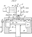
- FIG. 1 there is seen a schematic diagram of an exemplary hydrogen-ion producing reactor, generally illustrated as 10 , communicating with a CVD apparatus, generally illustrated as 30 , through a conduit 12 having a flow control valve 13 .
- a hydrogen-ion producing reactor generally illustrated as 10
- a CVD apparatus generally illustrated as 30
- a conduit 12 having a flow control valve 13 .
- water (H 2 O) and/or steam and ozone (O 3 ) are introduced into reactor chamber 14 through lines 16 and 18 , respectively.
- Reactor chamber 14 is preferably at a pressure ranging from about 2 Torr to about 400 Torr, more preferably from about 80 Torr to about 200 Torr, most preferably from about 100 Torr to about 150 Torr.
- the reactor chamber 14 is preferably at a temperature ranging from about 50°C to about 250°C, more preferably from about 100°C to about 200°C, most preferably from about 150°C to about 160°C.
- a radiation transmission window 22 is coupled to reactor chamber 14 such that a suitable radiation source may transmit radiation into reactor chamber 14 in order to enhance the decomposition rate of the injected ozone molecules.
- radiation transmission window 22 may be a quartz window suitable to transmit ultraviolet radiation into reactor chamber 14.
- radiation may be introduced directly from a mercury arc lamp 24 at radiation transmission window 22. It should be appreciated that any suitable radiation source or configuration may be substituted for mercury arc lamp 24 .
- a radiation source may have a wavelength radiation spectrum containing a wavelength line ranging from about 200 nm to about 300 nm, preferably about a wavelength line containing about 254 nm line corresponding to strong ozone absorption.
- mercury arc lamp 24 is activated such that ultraviolet radiation having an approximate wavelength of 254 nm is directed at the ozone/water mixture in the reactor chamber 14 .
- the water rich gas phase ozone molecules are caused to decompose and form oxygen molecules and atomic oxygen (O*) in 1 D state.
- O* atomic oxygen
- hydroxyl radicals are produced via the ultraviolet photolysis of ozone to produce electronically excited singlet oxygen atoms: O 3 + h ⁇ ( ⁇ 310) ⁇ O( 1 D) + O 2
- the primary fate of the singlet oxygen atoms is collistional deactivation to the triplet ground state: O 3 ( 1 D)+M ⁇ O+M where M is the cold reactor wall, as stated in the Kirk-Othmer, Encyclopedia of Chemical Technology, Vol. 17, p. 953-994, Fourth Edition published by John Wiley & Sons (New York, 1996), incorporated herein by reference thereto.
- the ultraviolet photolysis of O 3 ⁇ H 2 O clusters also provide a source of hydroxyl radicals and/or hydrogen peroxide: O 3 ⁇ H 2 O + h ⁇ ⁇ 2OH + O 2 O 3 ⁇ H 2 O + h ⁇ ⁇ H 2 O 2 + O 2 Reaction 1 (R1) is energetically possible for wavelengths of light shorter than 665 nm, while reaction 2 (R2) is exothermic even without the absorption of light.
- the ground state O atoms produced in the ultraviolet photolysis of ozone have up to 22.2 kcal mol -1 of translational energy to overcome the activation barriers necessary to abstract a hydrogen atom from water or to insert into the water molecule to form H 2 O 2 .
- reactions R1 and R2 may be preferential over other reactions, such as combination with O 2 to reform ozone.
- hydrogen peroxide (H 2 O 2 ) produced by reaction R2 above, or otherwise provided for reactor chamber 14 breaks down or decomposes in the presence of ultraviolet light into hydroxyl ions, and thus may provide an additional gas-phase source of hydroxyl radicals: H 2 O 2 + h ⁇ ⁇ 2OH
- hydrogen peroxide preferably gaseous H 2 O 2 solely, or hydrogen peroxide in combination with ozone and/or water and/or water vapor or steam
- hydrogen peroxide reduces to hydroxyl radicals when contacted by ultraviolet radiation.
- valve 13 is opened and hydroxyl radicals in a gas phase flow out of the reactor chamber 14 and into conduit 12 .
- the hydroxyl radical gas phase comprises a temperature ranging from about 80°C to about 175°C, more preferably from about 100°C to about 150°C.
- the hydroxyl radical gas phase also comprises a pressure ranging from about 2 Torr to about 400 Torr, preferably from about 50 Torr, to about 250 Torr, more preferably from about 100 Torr to about 150 Torr.
- a precursor e.g., TEOS
- an inert carrier gas such as nitrogen, argon and helium (or any other suitable inert carrier gas such as krypton, radon, and xenon)
- the hydroxyl radicals immediately start reacting with the precursor within conduit 12 before the mixture of precursor and hydroxyl radicals (along with inert carrier gas, unreacted water, oxygen and ozone) is introduced into the CVD apparatus 30 .
- the hydroxyl radicals are reacting with the precursor, causing essentially instantaneous decomposition of the precursor as it enters the CVD apparatus 30 .
- the precursor e.g., TEOS
- the precursor flows from conduit 29 into a conduit 32 which communicates with the CVD apparatus 30 in order to cause the gaseous precursor to come in contact with the gaseous hydroxyl radicals flowing out of conduit 12 in the CVD apparatus 30 such that the reaction of the precursor and the hydroxyl radicals, as well as decomposition of the precursor, commences immediately within the CVD apparatus 30 .
- the produced hydroxyl radicals (along with unreacted water, oxygen and ozone) flow directly into the CVD apparatus 30 .
- CVD apparatus 30 includes an enclosure assembly 36 housing a vacuum chamber 38 with a gas reaction area 40 .
- a gas distribution plate 42 is provided above the gas reaction area 40 for dispersing reactive gases through perforated holes in plate 42 to a wafer (not shown) that rests on a vertically movable heater 44 (also referred to as wafer support pedestal or susceptor).
- CVD apparatus 30 further includes a heater/lift assembly 46 for heating the wafer supported on heater 44. Heater/lift assembly 46 also can be controllably moved between a lower loading/off-loading position and an upper processing position indicated by dotted line 48 which is closely adjacent to plate 42, as shown in Fig. 1.
- a center board (not shown) includes sensors for providing information on the position of the wafer.
- Heater 44 includes resistively-heated components enclosed in a ceramic, preferably aluminum nitride or anodized aluminum.
- a ceramic preferably aluminum nitride or anodized aluminum.
- all surfaces of heater 44 exposed to vacuum chamber 38 are made of a ceramic material, such as aluminum oxide (Al 2 O 3 or alumina) or aluminum nitride.
- heater 44 and the wafer are in processing position 48, they are surrounded by a chamber liner 50 along the inside walls 52 of CVD apparatus 30 and by an annular pumping channel 54 , formed by chamber liner 56 and a top portion of vacuum chamber 38 .
- chamber liner 50 preferably comprises a ceramic material, such a alumina or aluminum nitride, which serves to lower the temperature gradient between resistively-heated heater 44 (high temperature) and chamber walls 52 , which are at a much lower temperature relative to heater 44 .
- valve 13 is subsequently opened causing the formed gaseous hydroxyl radicals (along with unreacted water/steam, oxygen and ozone) to either flow directly into the CVD apparatus 30 via conduit 12 as best shown in Fig. 2, or to be admixed within conduit 29 with gaseous TEOS (i.e., the precursor), along with its associated inert carrier gas (e.g., nitrogen or argon), flowing into conduit 12 via conduit 29 .
- gaseous TEOS i.e., the precursor
- inert carrier gas e.g., nitrogen or argon
- the formed gaseous hydroxyl radicals along with unreacted water/steam, oxygen and ozone comprise at least about 10% by volume hydroxyl radicals, preferably from about 10% by volume to about 30% by volume hydroxyl radicals, more preferably from about 15% by volume to about 25% by volume hydroxyl radicals, most preferably from about 17% by volume to about 23% by volume (e.g., about 20% by volume) hydroxyl radicals. Because the hydroxyl radicals have a short half-life (e.g., from about 2 secs. to about 14 secs.), once the hydroxyl radicals are produced in the reactor chamber 14 , they are subsequently delivered into the CVD apparatus 30 of Fig. 2 for the embodiment of the invention of Fig. 2, within about 30 secs.
- a short half-life e.g., from about 2 secs. to about 14 secs.
- the hydroxyl radicals are subsequently delivered into contact with TEOS (i.e., the precursor) within conduit 12 within about 30 secs. after formation, preferably into contact with TEOS within a time period ranging from about 1 sec. to about 30 secs. after formation, more preferably into contact with TEOS within a time period ranging from about 1 sec. to about 30 secs. after formation, more preferably into contact with TEOS within a time period ranging from about 2 secs. to about 12 secs. after formation, most preferably into contact with TEOS within a time period ranging from about 2 secs. to about 8 secs after formation.
- TEOS i.e., the precursor
- hydroxyl radical gas (along with associated unreacted water/steam, oxygen, and ozone) is flowed out of reactor chamber 14 , and gaseous TEOS (along with inert carrier gas) is flowed through conduit 29 at rates such that a stoichiometric amount of hydroxyl radical gas is available to react with TEOS gas.
- gaseous TEOS (along with inert gas) comes into contact with and mixes with gaseous hydroxyl radicals (along with unreacted water/steam, oxygen and ozone), either in conduit 12 for the embodiment of the invention of Fig 1 or within the CVD apparatus 30 for the embodiment of the invention of Fig.
- the resulting mixture comprises, or consists of, or consists essentially of, from about 50% to about 95% by volume TEOS (along with inert gas) and from about 5% by volume to about 50% by volume hydroxyl radicals (along with unreacted water/steam, oxygen and ozone), preferably from about 55% to about 90% by volume TEOS (along with inert gas) and from about 10% to about 45% by volume hydroxyl radicals (along with unreacted water/steam, oxygen and ozone), more preferably from about 60% to about 85% by volume TEOS (along with inert gas) and from about 15% to about 40% by volume hydroxyl radicals (along with unreacted water/steam, oxygen and ozone), most preferably from about 65% to about 80% by volume TEOS (along with inert gas) and from about 20% to about 35% by volume hydroxyl radicals (along with unreacted water/steam, oxygen and ozone).
- gaseous TEOS (along with inert gas) comes into contact with and mixes with gaseous hydroxyl radicals (along with unreacted water/steam, oxygen and ozone) either for the embodiment of the invention of Fig. 1 or for the embodiment of the invention of Fig.
- the resulting mixture comprises, or consists of, or consists essentially of, from about 5% to about 15% by volume TEOS gas, from about 30% to about 50% by volume inert gas, from about 5% to about 15% by volume hydroxyl radical gas, from about 0% to about 20% by volume of a water-containing agent (e.g., water), from about 10% to about 30% by volume oxygen, from about 0% to about 5% by volume ozone; more preferably from about 10% to about 15% by volume TEOS gas, from about 30% to about 40% by volume inert gas, from about 10% to about 15% by volume hydroxyl radical gas, from about 0% to about 10% by volume of a water-containing agent (e.g., water), from about 10% to about 30% by volume oxygen, from about 0% to about 10% by volume ozone; most preferably from about 12% to about 15% by volume TEOS gas, from about 40% to about 45% by volume inert gas, from about 12% to about 15% by volume hydroxyl radical gas, from about 0% to about 8% by volume
- gaseous TEOS (along with inert carrier gas) and hydroxyl radicals (along with unreacted water/steam, oxygen and ozone) are mixed together, either for the embodiment of the invention of Fig. 1 or for the embodiment of the invention or of Fig. 2, the mixture is delivered to plate 42 .
- gas supplied to plate 42 is vented toward the wafer surface (as indicated by arrows 60 ), where it may be uniformly distributed radially across the wafer surface, typically in a laminar flow.
- Purging gas may be delivered into vacuum chamber 38 from an inlet port or tube (not shown) through the bottom wall of enclosure assembly 36 .
- the purging gas flows upward past heater 44 and to an annular pumping channel 54 .
- An exhaust system then exhausts the gas (as indicated by arrows 64 ) into the annular pumping channel 54 and through an exhaust line 68 by a vacuum pump system (not shown). Exhaust gases and residues are preferably released from annular pumping channel 54 through exhaust line 68 at a rate controlled by a throttle valve system 70 .
- thermal CVD processes supply reactive gases to the substrate surface where heat-induced chemical reactions (homogeneous or heterogeneous) take place to produce a desired film.
- heat is distributed by resistively-heated heater 44 that is capable of reaching temperatures as high as about 400-800°C.
- Such heat distribution provides uniform, rapid thermal heating of the wafer for effecting deposition, reflow and/or drive-in, cleaning, and/or seasoning/gettering steps in a multiple-step process in situ in vacuum chamber 38.
- a controlled plasma may be formed adjacent to the wafer by RF energy applied to gas distribution plate 42 from an RF power supply (not shown).
- the RF power supply can supply either single frequency RF power to plate 42 or mixed frequency RF power to plate 42 and the lower RF electrode to enhance the decomposition of reactive species introduced into process chamber 38.
- some of the components of vapor deposition apparatus 30 would have to be modified to accommodate the RF energy.
- a method for depositing a layer on a substrate in a chemical vapor deposition reaction zone comprising introducing a precursor, (e.g. TEOS) into a chemical vapor deposition reaction zone containing a substrate, and introducing hydroxyl radical in a gas phase into the chemical vapor deposition reaction zone for reacting with the precursor to form a deposition layer on the substrate.
- a precursor e.g. TEOS
- the hydroxyl radical gas phase preferably comprises at least about 10% by volume hydroxyl radicals, and the temperature of the gas phase preferably ranges from about 100°C to about 150°C.
- An inert gas is typically employed as a carrier gas for the precursor.
- the method for depositing a layer additionally comprises producing the hydroxyl radicals prior to the introducing hydroxyl radicals into the chemical vapor deposition reaction zone.
- hydroxyl radicals are introduced at a pressure ranging from about 100 Torrance to about 200 Torrance.
- a method for forming a deposition layer in a chemical vapor deposition reactor comprising the steps of (a) producing hydroxyl radicals; (b) admixing the produced hydroxyl radicals with a precursor (e.g. a processing gas such as an organometallic processing gas) to produce a hydroxyl radicals-precursor mixture; and (c) introducing the hydroxyl radicals-precursor mixture into the chemical vapor deposition reactor to form a deposition layer.
- a precursor e.g. a processing gas such as an organometallic processing gas
- the producing of hydroxyl radicals preferably comprises introducing a water-containing agent (e.g., water) and ozone into a hydroxyl radical-producing reactor; and directing ultraviolet radiation into the hydroxyl radical-producing reactor to cause oxygen atoms to form from the ozone and react with the water-containing agent to produce hydroxyl radicals.
- the method additional comprises removing, prior to the admixing step (b), hydroxyl radicals from the hydroxyl radical-producing reactor.
- the admixing of hydroxyl radicals with the precursor causes the hydroxyl radicals to react with the precursor.
- the hydroxyl radicals and the precursor are reacting as the hydroxyl radicals-precursor mixture is being introduced into the chemical vapor deposition reactor.
- a chemical vapor deposition reactor including a CVD reactor chamber, for forming deposition films comprising a chemical vapor deposition reactor chamber; and a source of hydroxyl ion gas coupled to the chemical vapor deposition reactor chamber and including hydroxyl ion gas flowing or introducing into the chemical vapor deposition reactor chamber.
- a pedestal is disposed in the reactor chamber for supporting substrates in the reactor chamber.
- the chemical vapor deposition reactor also comprises a processing power source; a processing gas-introducing assembly engaged to the reactor chamber for introducing a processing gas into the reactor chamber; and a processing power-transmitting member disposed in proximity to the reactor chamber and connected to the processing power source for transmitting power into the reactor interior for forming deposition films.
- the source of hydroxyl ion gas comprises a hydroxyl-ion producing reactor having at least one inlet port; a source of water coupled to the at least one inlet port; a source of ozone gas also coupled to the at least one inlet port; and a source of ultraviolet radiation oriented to direct ultraviolet radiation into the hydroxyl-ion producing reactor.
Landscapes
- Chemical & Material Sciences (AREA)
- Engineering & Computer Science (AREA)
- Materials Engineering (AREA)
- Metallurgy (AREA)
- Organic Chemistry (AREA)
- General Chemical & Material Sciences (AREA)
- Chemical Kinetics & Catalysis (AREA)
- Mechanical Engineering (AREA)
- Crystallography & Structural Chemistry (AREA)
- Inorganic Chemistry (AREA)
- Chemical Vapour Deposition (AREA)
- Formation Of Insulating Films (AREA)
- Electrodes Of Semiconductors (AREA)
- Cleaning Or Drying Semiconductors (AREA)
Applications Claiming Priority (2)
| Application Number | Priority Date | Filing Date | Title |
|---|---|---|---|
| US557079 | 1975-03-10 | ||
| US09/557,079 US6596343B1 (en) | 2000-04-21 | 2000-04-21 | Method and apparatus for processing semiconductor substrates with hydroxyl radicals |
Publications (3)
| Publication Number | Publication Date |
|---|---|
| EP1148150A2 true EP1148150A2 (de) | 2001-10-24 |
| EP1148150A3 EP1148150A3 (de) | 2006-06-28 |
| EP1148150B1 EP1148150B1 (de) | 2009-09-16 |
Family
ID=24223973
Family Applications (1)
| Application Number | Title | Priority Date | Filing Date |
|---|---|---|---|
| EP01303631A Expired - Lifetime EP1148150B1 (de) | 2000-04-21 | 2001-04-20 | Verfahren und Vorrichtung zur Behandlung von Halbleitersubstraten mit Hydroxylradikalen |
Country Status (6)
| Country | Link |
|---|---|
| US (2) | US6596343B1 (de) |
| EP (1) | EP1148150B1 (de) |
| JP (1) | JP4739577B2 (de) |
| KR (1) | KR100715074B1 (de) |
| AT (1) | ATE443164T1 (de) |
| DE (1) | DE60139912D1 (de) |
Cited By (2)
| Publication number | Priority date | Publication date | Assignee | Title |
|---|---|---|---|---|
| EP2249413A3 (de) * | 2002-04-01 | 2011-02-02 | Konica Corporation | Träger und organisches elektrolumineszentes Bauelement mit einem solchen Träger |
| DE102011001642A1 (de) * | 2011-03-29 | 2012-10-04 | Universität Bremen | Verfahren und Vorrichtung zum Herstellen einer Polymerschicht |
Families Citing this family (53)
| Publication number | Priority date | Publication date | Assignee | Title |
|---|---|---|---|---|
| US6596343B1 (en) * | 2000-04-21 | 2003-07-22 | Applied Materials, Inc. | Method and apparatus for processing semiconductor substrates with hydroxyl radicals |
| JP2002110611A (ja) * | 2000-10-04 | 2002-04-12 | Texas Instr Japan Ltd | 半導体ウェハの洗浄方法及び装置 |
| US20020127763A1 (en) * | 2000-12-28 | 2002-09-12 | Mohamed Arafa | Sidewall spacers and methods of making same |
| US8749054B2 (en) | 2010-06-24 | 2014-06-10 | L. Pierre de Rochemont | Semiconductor carrier with vertical power FET module |
| JP4843611B2 (ja) | 2004-10-01 | 2011-12-21 | デ,ロシェモント,エル.,ピエール | セラミックアンテナモジュール及びその製造方法 |
| US8163087B2 (en) * | 2005-03-31 | 2012-04-24 | Tokyo Electron Limited | Plasma enhanced atomic layer deposition system and method |
| JP4808436B2 (ja) * | 2005-05-18 | 2011-11-02 | 株式会社神戸製鋼所 | 機能膜形成方法 |
| US8350657B2 (en) | 2005-06-30 | 2013-01-08 | Derochemont L Pierre | Power management module and method of manufacture |
| CN101213638B (zh) | 2005-06-30 | 2011-07-06 | L·皮尔·德罗什蒙 | 电子元件及制造方法 |
| JP2007194582A (ja) * | 2005-12-20 | 2007-08-02 | Tokyo Electron Ltd | 高誘電体薄膜の改質方法及び半導体装置 |
| US7763917B2 (en) * | 2006-01-24 | 2010-07-27 | De Rochemont L Pierre | Photovoltaic devices with silicon dioxide encapsulation layer and method to make same |
| US8354294B2 (en) | 2006-01-24 | 2013-01-15 | De Rochemont L Pierre | Liquid chemical deposition apparatus and process and products therefrom |
| US8635971B2 (en) * | 2006-03-31 | 2014-01-28 | Lam Research Corporation | Tunable uniformity in a plasma processing system |
| US20080020549A1 (en) * | 2006-07-20 | 2008-01-24 | Qc Solutions, Inc. | Method and apparatus for forming an oxide layer on semiconductors |
| US20090305515A1 (en) * | 2008-06-06 | 2009-12-10 | Dustin Ho | Method and apparatus for uv curing with water vapor |
| US7959598B2 (en) | 2008-08-20 | 2011-06-14 | Asante Solutions, Inc. | Infusion pump systems and methods |
| US8952858B2 (en) | 2009-06-17 | 2015-02-10 | L. Pierre de Rochemont | Frequency-selective dipole antennas |
| US8922347B1 (en) | 2009-06-17 | 2014-12-30 | L. Pierre de Rochemont | R.F. energy collection circuit for wireless devices |
| US20110151677A1 (en) | 2009-12-21 | 2011-06-23 | Applied Materials, Inc. | Wet oxidation process performed on a dielectric material formed from a flowable cvd process |
| US8465587B2 (en) * | 2009-12-30 | 2013-06-18 | Cbl Technologies, Inc. | Modern hydride vapor-phase epitaxy system and methods |
| KR101143631B1 (ko) * | 2010-04-30 | 2012-05-09 | 에스케이하이닉스 주식회사 | 소자분리층을 포함하는 반도체 소자 형성 방법 |
| US8552708B2 (en) | 2010-06-02 | 2013-10-08 | L. Pierre de Rochemont | Monolithic DC/DC power management module with surface FET |
| US9023493B2 (en) | 2010-07-13 | 2015-05-05 | L. Pierre de Rochemont | Chemically complex ablative max-phase material and method of manufacture |
| EP2609626B1 (de) | 2010-08-23 | 2024-04-03 | L. Pierre De Rochemont | Power-fet mit einem resonanz-transistor-gate |
| CN103415925A (zh) | 2010-11-03 | 2013-11-27 | L·皮尔·德罗什蒙 | 具有单片集成的量子点器件的半导体芯片载体及其制造方法 |
| KR101373061B1 (ko) * | 2013-03-04 | 2014-03-17 | 백경림 | 지퍼가 구비된 모자 |
| US9561324B2 (en) | 2013-07-19 | 2017-02-07 | Bigfoot Biomedical, Inc. | Infusion pump system and method |
| JP6354539B2 (ja) * | 2014-11-25 | 2018-07-11 | 東京エレクトロン株式会社 | 基板処理装置、基板処理方法、記憶媒体 |
| KR101727259B1 (ko) | 2015-03-18 | 2017-04-17 | 연세대학교 산학협력단 | 산화물 박막 형성 방법 및 산화물 박막 형성 장치 |
| TWI570263B (zh) * | 2015-08-10 | 2017-02-11 | 炬力奈米科技有限公司 | 光輔助原子層沉積方法 |
| WO2017123525A1 (en) | 2016-01-13 | 2017-07-20 | Bigfoot Biomedical, Inc. | User interface for diabetes management system |
| US10806859B2 (en) | 2016-01-14 | 2020-10-20 | Bigfoot Biomedical, Inc. | Adjusting insulin delivery rates |
| HK1256995A1 (zh) | 2016-01-14 | 2019-10-11 | Bigfoot Biomedical, Inc. | 药物输送设备、系统和方法中的阻塞解决方案 |
| US12383166B2 (en) | 2016-05-23 | 2025-08-12 | Insulet Corporation | Insulin delivery system and methods with risk-based set points |
| US10363374B2 (en) | 2016-05-26 | 2019-07-30 | Insulet Corporation | Multi-dose drug delivery device |
| US10858727B2 (en) | 2016-08-19 | 2020-12-08 | Applied Materials, Inc. | High density, low stress amorphous carbon film, and process and equipment for its deposition |
| US11096624B2 (en) | 2016-12-12 | 2021-08-24 | Bigfoot Biomedical, Inc. | Alarms and alerts for medication delivery devices and systems |
| US10881792B2 (en) | 2017-01-13 | 2021-01-05 | Bigfoot Biomedical, Inc. | System and method for adjusting insulin delivery |
| US11033682B2 (en) | 2017-01-13 | 2021-06-15 | Bigfoot Biomedical, Inc. | Insulin delivery methods, systems and devices |
| US10758675B2 (en) | 2017-01-13 | 2020-09-01 | Bigfoot Biomedical, Inc. | System and method for adjusting insulin delivery |
| US10500334B2 (en) | 2017-01-13 | 2019-12-10 | Bigfoot Biomedical, Inc. | System and method for adjusting insulin delivery |
| US10583250B2 (en) | 2017-01-13 | 2020-03-10 | Bigfoot Biomedical, Inc. | System and method for adjusting insulin delivery |
| EP3568860B1 (de) | 2017-01-13 | 2025-12-10 | Insulet Corporation | Insulinverabreichungsverfahren, -systeme und -vorrichtungen |
| KR101987705B1 (ko) * | 2017-02-28 | 2019-06-11 | (주)엔피홀딩스 | Uv 램프를 이용한 기판 세정 노즐 |
| USD874471S1 (en) | 2017-06-08 | 2020-02-04 | Insulet Corporation | Display screen with a graphical user interface |
| USD928199S1 (en) | 2018-04-02 | 2021-08-17 | Bigfoot Biomedical, Inc. | Medication delivery device with icons |
| US12562251B1 (en) | 2018-05-09 | 2026-02-24 | Bigfoot Biomedical, Inc. | Computing architecture for assuring the provenance of medication therapy related parameters, and related systems, methods and devices |
| USD920343S1 (en) | 2019-01-09 | 2021-05-25 | Bigfoot Biomedical, Inc. | Display screen or portion thereof with graphical user interface associated with insulin delivery |
| USD977502S1 (en) | 2020-06-09 | 2023-02-07 | Insulet Corporation | Display screen with graphical user interface |
| CA3201894A1 (en) | 2020-12-18 | 2022-06-23 | Matthew Alles | Integration of a medicament delivery device with a smartwatch and a vehicle infotainment system |
| US12514980B2 (en) | 2021-06-30 | 2026-01-06 | Insulet Corporation | Adjustment of medicament delivery by a medicament delivery device based on menstrual cycle phase |
| US12521486B2 (en) | 2021-07-16 | 2026-01-13 | Insulet Corporation | Method for modification of insulin delivery during pregnancy in automatic insulin delivery systems |
| EP4646726A1 (de) | 2023-01-06 | 2025-11-12 | Insulet Corporation | Automatisch oder manuell initiierte mahlzeitbolusabgabe mit anschliessender automatischer sicherheitseinschränkungsrelaxation |
Citations (3)
| Publication number | Priority date | Publication date | Assignee | Title |
|---|---|---|---|---|
| US5665640A (en) | 1994-06-03 | 1997-09-09 | Sony Corporation | Method for producing titanium-containing thin films by low temperature plasma-enhanced chemical vapor deposition using a rotating susceptor reactor |
| US6030460A (en) | 1996-05-24 | 2000-02-29 | Lsi Logic Corporation | Method and apparatus for forming dielectric films |
| EP1063692A1 (de) | 1999-06-22 | 2000-12-27 | Applied Materials, Inc. | Verfahren zur Abscheidung eines Films mit niedriger Dielektrizitätskonstante |
Family Cites Families (20)
| Publication number | Priority date | Publication date | Assignee | Title |
|---|---|---|---|---|
| US5279705A (en) * | 1990-11-28 | 1994-01-18 | Dainippon Screen Mfg. Co., Ltd. | Gaseous process for selectively removing silicon nitride film |
| US5126111A (en) * | 1990-12-05 | 1992-06-30 | Nutech Energy Systems Inc. | Fluid purification |
| JP2989063B2 (ja) * | 1991-12-12 | 1999-12-13 | キヤノン株式会社 | 薄膜形成装置および薄膜形成方法 |
| JP3084497B2 (ja) * | 1992-03-25 | 2000-09-04 | 東京エレクトロン株式会社 | SiO2膜のエッチング方法 |
| JP2870307B2 (ja) * | 1992-07-10 | 1999-03-17 | 日本電気株式会社 | 移動通信制御局および多重接続方式 |
| JPH086181B2 (ja) * | 1992-11-30 | 1996-01-24 | 日本電気株式会社 | 化学気相成長法および化学気相成長装置 |
| US5395522A (en) * | 1993-02-23 | 1995-03-07 | Anatel Corporation | Apparatus for removal of organic material from water |
| FR2734402B1 (fr) * | 1995-05-15 | 1997-07-18 | Brouquet Pierre | Procede pour l'isolement electrique en micro-electronique, applicable aux cavites etroites, par depot d'oxyde a l'etat visqueux et dispositif correspondant |
| JPH09232296A (ja) * | 1996-02-23 | 1997-09-05 | Mitsubishi Electric Corp | 半導体装置の製造装置および製造方法 |
| WO1997031391A1 (en) * | 1996-02-23 | 1997-08-28 | Ebara Corporation | Chemical vapor deposition method and chemical vapor deposition apparatus |
| US5792369A (en) * | 1996-04-04 | 1998-08-11 | Johnson; Dennis E. J. | Apparatus and processes for non-chemical plasma ion disinfection of water |
| JPH1081588A (ja) * | 1996-09-05 | 1998-03-31 | Matsushita Electric Ind Co Ltd | 半導体ダイヤモンド及びその形成方法 |
| JPH10321610A (ja) * | 1997-03-19 | 1998-12-04 | Fujitsu Ltd | 半導体装置の製造方法 |
| US6086679A (en) * | 1997-10-24 | 2000-07-11 | Quester Technology, Inc. | Deposition systems and processes for transport polymerization and chemical vapor deposition |
| US6020458A (en) * | 1997-10-24 | 2000-02-01 | Quester Technology, Inc. | Precursors for making low dielectric constant materials with improved thermal stability |
| US6095085A (en) * | 1998-08-20 | 2000-08-01 | Micron Technology, Inc. | Photo-assisted remote plasma apparatus and method |
| FI108375B (fi) * | 1998-09-11 | 2002-01-15 | Asm Microchemistry Oy | Menetelmõ eristõvien oksidiohutkalvojen valmistamiseksi |
| US6200387B1 (en) * | 1998-10-30 | 2001-03-13 | Dangsheng P. E. Ni | Method and system for processing substrates using nebulized chemicals created by heated chemical gases |
| US6200893B1 (en) * | 1999-03-11 | 2001-03-13 | Genus, Inc | Radical-assisted sequential CVD |
| US6596343B1 (en) * | 2000-04-21 | 2003-07-22 | Applied Materials, Inc. | Method and apparatus for processing semiconductor substrates with hydroxyl radicals |
-
2000
- 2000-04-21 US US09/557,079 patent/US6596343B1/en not_active Expired - Lifetime
-
2001
- 2001-04-20 AT AT01303631T patent/ATE443164T1/de not_active IP Right Cessation
- 2001-04-20 DE DE60139912T patent/DE60139912D1/de not_active Expired - Lifetime
- 2001-04-20 EP EP01303631A patent/EP1148150B1/de not_active Expired - Lifetime
- 2001-04-21 KR KR1020010021607A patent/KR100715074B1/ko not_active Expired - Fee Related
- 2001-04-23 JP JP2001163437A patent/JP4739577B2/ja not_active Expired - Fee Related
-
2003
- 2003-06-02 US US10/453,227 patent/US20030221621A1/en not_active Abandoned
Patent Citations (3)
| Publication number | Priority date | Publication date | Assignee | Title |
|---|---|---|---|---|
| US5665640A (en) | 1994-06-03 | 1997-09-09 | Sony Corporation | Method for producing titanium-containing thin films by low temperature plasma-enhanced chemical vapor deposition using a rotating susceptor reactor |
| US6030460A (en) | 1996-05-24 | 2000-02-29 | Lsi Logic Corporation | Method and apparatus for forming dielectric films |
| EP1063692A1 (de) | 1999-06-22 | 2000-12-27 | Applied Materials, Inc. | Verfahren zur Abscheidung eines Films mit niedriger Dielektrizitätskonstante |
Cited By (3)
| Publication number | Priority date | Publication date | Assignee | Title |
|---|---|---|---|---|
| EP2249413A3 (de) * | 2002-04-01 | 2011-02-02 | Konica Corporation | Träger und organisches elektrolumineszentes Bauelement mit einem solchen Träger |
| DE102011001642A1 (de) * | 2011-03-29 | 2012-10-04 | Universität Bremen | Verfahren und Vorrichtung zum Herstellen einer Polymerschicht |
| DE102011001642B4 (de) * | 2011-03-29 | 2014-12-31 | Universität Bremen | Verfahren zum Herstellen einer Polymerschicht |
Also Published As
| Publication number | Publication date |
|---|---|
| KR20010098803A (ko) | 2001-11-08 |
| DE60139912D1 (de) | 2009-10-29 |
| EP1148150B1 (de) | 2009-09-16 |
| JP2002064095A (ja) | 2002-02-28 |
| US20030221621A1 (en) | 2003-12-04 |
| ATE443164T1 (de) | 2009-10-15 |
| US6596343B1 (en) | 2003-07-22 |
| JP4739577B2 (ja) | 2011-08-03 |
| KR100715074B1 (ko) | 2007-05-07 |
| EP1148150A3 (de) | 2006-06-28 |
Similar Documents
| Publication | Publication Date | Title |
|---|---|---|
| US6596343B1 (en) | Method and apparatus for processing semiconductor substrates with hydroxyl radicals | |
| US5710079A (en) | Method and apparatus for forming dielectric films | |
| US7238616B2 (en) | Photo-assisted method for semiconductor fabrication | |
| US6649545B2 (en) | Photo-assisted remote plasma apparatus and method | |
| US8481403B1 (en) | Flowable film dielectric gap fill process | |
| JP5401309B2 (ja) | ギャップ充填と共形のフィルムの適用のために低k膜を堆積させ硬化する方法 | |
| JP3218304B2 (ja) | 高誘電薄膜製造法 | |
| JPH0831454B2 (ja) | 半導体装置の製造方法 | |
| US20010012700A1 (en) | Semiconductor processing methods of chemical vapor depositing sio2 on a substrate | |
| JPH09172008A (ja) | Sacvd酸化物膜とpecvd酸化物膜との間に良好な界面を形成する方法及び装置 | |
| JPH03286531A (ja) | シリコン酸化膜の形成方法 | |
| US5693377A (en) | Method of reducing carbon incorporation into films produced by chemical vapor deposition involving titanium organometallic and metal-organic precursor compounds | |
| US6040010A (en) | Catalytic breakdown of reactant gases in chemical vapor deposition | |
| KR100474565B1 (ko) | 소스 가스 공급 방법 및 장치 | |
| US6335277B2 (en) | Method for forming metal nitride film | |
| US6110543A (en) | Process for making compound films | |
| US5849644A (en) | Semiconductor processing methods of chemical vapor depositing SiO2 on a substrate | |
| US6090725A (en) | Method for preventing bubble defects in BPSG film | |
| US20030087043A1 (en) | Low k dielectric film deposition process | |
| JPH05299523A (ja) | 絶縁膜の形成方法およびその装置 | |
| JP2786224B2 (ja) | 薄膜作製装置および方法 | |
| JPH0793298B2 (ja) | 半導体装置の形成方法 | |
| JPH05243214A (ja) | 半導体基板の上にシリコン酸化膜を形成する装置 | |
| JPH08134650A (ja) | Cvd膜形成方法及び装置 | |
| JPH03225827A (ja) | 絶縁膜の製造方法 |
Legal Events
| Date | Code | Title | Description |
|---|---|---|---|
| PUAI | Public reference made under article 153(3) epc to a published international application that has entered the european phase |
Free format text: ORIGINAL CODE: 0009012 |
|
| AK | Designated contracting states |
Kind code of ref document: A2 Designated state(s): AT BE CH CY DE DK ES FI FR GB GR IE IT LI LU MC NL PT SE TR |
|
| AX | Request for extension of the european patent |
Free format text: AL;LT;LV;MK;RO;SI |
|
| RIN1 | Information on inventor provided before grant (corrected) |
Inventor name: YIEH, ELLIE Inventor name: POKHAMA, HIMANSHU Inventor name: NEMANI, SRINIVAS D. Inventor name: CHEN, CHEN-AN Inventor name: CAMPANA, FRANCIMAR Inventor name: XIA, LI-QUN Inventor name: CHANDRAN, SHANKAR |
|
| PUAL | Search report despatched |
Free format text: ORIGINAL CODE: 0009013 |
|
| AK | Designated contracting states |
Kind code of ref document: A3 Designated state(s): AT BE CH CY DE DK ES FI FR GB GR IE IT LI LU MC NL PT SE TR |
|
| AX | Request for extension of the european patent |
Extension state: AL LT LV MK RO SI |
|
| RIC1 | Information provided on ipc code assigned before grant |
Ipc: C30B 25/08 20060101ALI20060523BHEP Ipc: H01L 21/285 20060101ALI20060523BHEP Ipc: C23C 16/48 20060101ALI20060523BHEP Ipc: C23C 16/40 20060101AFI20010828BHEP Ipc: H01L 21/205 20060101ALI20060523BHEP Ipc: H01L 21/316 20060101ALI20060523BHEP |
|
| 17P | Request for examination filed |
Effective date: 20061120 |
|
| AKX | Designation fees paid |
Designated state(s): AT BE CH CY DE DK ES FI FR GB GR IE IT LI LU MC NL PT SE TR |
|
| 17Q | First examination report despatched |
Effective date: 20070222 |
|
| GRAP | Despatch of communication of intention to grant a patent |
Free format text: ORIGINAL CODE: EPIDOSNIGR1 |
|
| GRAS | Grant fee paid |
Free format text: ORIGINAL CODE: EPIDOSNIGR3 |
|
| GRAA | (expected) grant |
Free format text: ORIGINAL CODE: 0009210 |
|
| AK | Designated contracting states |
Kind code of ref document: B1 Designated state(s): AT BE CH CY DE DK ES FI FR GB GR IE IT LI LU MC NL PT SE TR |
|
| REG | Reference to a national code |
Ref country code: GB Ref legal event code: FG4D |
|
| REG | Reference to a national code |
Ref country code: CH Ref legal event code: EP |
|
| REG | Reference to a national code |
Ref country code: IE Ref legal event code: FG4D |
|
| REF | Corresponds to: |
Ref document number: 60139912 Country of ref document: DE Date of ref document: 20091029 Kind code of ref document: P |
|
| PG25 | Lapsed in a contracting state [announced via postgrant information from national office to epo] |
Ref country code: FI Free format text: LAPSE BECAUSE OF FAILURE TO SUBMIT A TRANSLATION OF THE DESCRIPTION OR TO PAY THE FEE WITHIN THE PRESCRIBED TIME-LIMIT Effective date: 20090916 Ref country code: SE Free format text: LAPSE BECAUSE OF FAILURE TO SUBMIT A TRANSLATION OF THE DESCRIPTION OR TO PAY THE FEE WITHIN THE PRESCRIBED TIME-LIMIT Effective date: 20090916 |
|
| PG25 | Lapsed in a contracting state [announced via postgrant information from national office to epo] |
Ref country code: NL Free format text: LAPSE BECAUSE OF FAILURE TO SUBMIT A TRANSLATION OF THE DESCRIPTION OR TO PAY THE FEE WITHIN THE PRESCRIBED TIME-LIMIT Effective date: 20090916 |
|
| NLV1 | Nl: lapsed or annulled due to failure to fulfill the requirements of art. 29p and 29m of the patents act | ||
| PG25 | Lapsed in a contracting state [announced via postgrant information from national office to epo] |
Ref country code: CY Free format text: LAPSE BECAUSE OF FAILURE TO SUBMIT A TRANSLATION OF THE DESCRIPTION OR TO PAY THE FEE WITHIN THE PRESCRIBED TIME-LIMIT Effective date: 20090916 |
|
| PG25 | Lapsed in a contracting state [announced via postgrant information from national office to epo] |
Ref country code: PT Free format text: LAPSE BECAUSE OF FAILURE TO SUBMIT A TRANSLATION OF THE DESCRIPTION OR TO PAY THE FEE WITHIN THE PRESCRIBED TIME-LIMIT Effective date: 20100118 Ref country code: ES Free format text: LAPSE BECAUSE OF FAILURE TO SUBMIT A TRANSLATION OF THE DESCRIPTION OR TO PAY THE FEE WITHIN THE PRESCRIBED TIME-LIMIT Effective date: 20091227 |
|
| PG25 | Lapsed in a contracting state [announced via postgrant information from national office to epo] |
Ref country code: BE Free format text: LAPSE BECAUSE OF FAILURE TO SUBMIT A TRANSLATION OF THE DESCRIPTION OR TO PAY THE FEE WITHIN THE PRESCRIBED TIME-LIMIT Effective date: 20090916 Ref country code: AT Free format text: LAPSE BECAUSE OF FAILURE TO SUBMIT A TRANSLATION OF THE DESCRIPTION OR TO PAY THE FEE WITHIN THE PRESCRIBED TIME-LIMIT Effective date: 20090916 |
|
| PLBE | No opposition filed within time limit |
Free format text: ORIGINAL CODE: 0009261 |
|
| STAA | Information on the status of an ep patent application or granted ep patent |
Free format text: STATUS: NO OPPOSITION FILED WITHIN TIME LIMIT |
|
| PG25 | Lapsed in a contracting state [announced via postgrant information from national office to epo] |
Ref country code: DK Free format text: LAPSE BECAUSE OF FAILURE TO SUBMIT A TRANSLATION OF THE DESCRIPTION OR TO PAY THE FEE WITHIN THE PRESCRIBED TIME-LIMIT Effective date: 20090916 |
|
| 26N | No opposition filed |
Effective date: 20100617 |
|
| PG25 | Lapsed in a contracting state [announced via postgrant information from national office to epo] |
Ref country code: GR Free format text: LAPSE BECAUSE OF FAILURE TO SUBMIT A TRANSLATION OF THE DESCRIPTION OR TO PAY THE FEE WITHIN THE PRESCRIBED TIME-LIMIT Effective date: 20091217 |
|
| PG25 | Lapsed in a contracting state [announced via postgrant information from national office to epo] |
Ref country code: MC Free format text: LAPSE BECAUSE OF NON-PAYMENT OF DUE FEES Effective date: 20100430 |
|
| REG | Reference to a national code |
Ref country code: CH Ref legal event code: PL |
|
| REG | Reference to a national code |
Ref country code: FR Ref legal event code: ST Effective date: 20101230 |
|
| PG25 | Lapsed in a contracting state [announced via postgrant information from national office to epo] |
Ref country code: IE Free format text: LAPSE BECAUSE OF NON-PAYMENT OF DUE FEES Effective date: 20100420 |
|
| PG25 | Lapsed in a contracting state [announced via postgrant information from national office to epo] |
Ref country code: LI Free format text: LAPSE BECAUSE OF NON-PAYMENT OF DUE FEES Effective date: 20100430 Ref country code: CH Free format text: LAPSE BECAUSE OF NON-PAYMENT OF DUE FEES Effective date: 20100430 |
|
| PG25 | Lapsed in a contracting state [announced via postgrant information from national office to epo] |
Ref country code: IT Free format text: LAPSE BECAUSE OF FAILURE TO SUBMIT A TRANSLATION OF THE DESCRIPTION OR TO PAY THE FEE WITHIN THE PRESCRIBED TIME-LIMIT Effective date: 20090916 |
|
| PG25 | Lapsed in a contracting state [announced via postgrant information from national office to epo] |
Ref country code: FR Free format text: LAPSE BECAUSE OF NON-PAYMENT OF DUE FEES Effective date: 20100430 |
|
| PG25 | Lapsed in a contracting state [announced via postgrant information from national office to epo] |
Ref country code: LU Free format text: LAPSE BECAUSE OF NON-PAYMENT OF DUE FEES Effective date: 20100420 |
|
| PG25 | Lapsed in a contracting state [announced via postgrant information from national office to epo] |
Ref country code: TR Free format text: LAPSE BECAUSE OF FAILURE TO SUBMIT A TRANSLATION OF THE DESCRIPTION OR TO PAY THE FEE WITHIN THE PRESCRIBED TIME-LIMIT Effective date: 20090916 |
|
| PGFP | Annual fee paid to national office [announced via postgrant information from national office to epo] |
Ref country code: GB Payment date: 20130326 Year of fee payment: 13 |
|
| PGFP | Annual fee paid to national office [announced via postgrant information from national office to epo] |
Ref country code: DE Payment date: 20130430 Year of fee payment: 13 |
|
| REG | Reference to a national code |
Ref country code: DE Ref legal event code: R119 Ref document number: 60139912 Country of ref document: DE |
|
| GBPC | Gb: european patent ceased through non-payment of renewal fee |
Effective date: 20140420 |
|
| REG | Reference to a national code |
Ref country code: DE Ref legal event code: R119 Ref document number: 60139912 Country of ref document: DE Effective date: 20141101 |
|
| PG25 | Lapsed in a contracting state [announced via postgrant information from national office to epo] |
Ref country code: DE Free format text: LAPSE BECAUSE OF NON-PAYMENT OF DUE FEES Effective date: 20141101 Ref country code: GB Free format text: LAPSE BECAUSE OF NON-PAYMENT OF DUE FEES Effective date: 20140420 |