EP1160872A2 - Dispositif semiconducteur avec une tranchée - Google Patents
Dispositif semiconducteur avec une tranchée Download PDFInfo
- Publication number
- EP1160872A2 EP1160872A2 EP01121361A EP01121361A EP1160872A2 EP 1160872 A2 EP1160872 A2 EP 1160872A2 EP 01121361 A EP01121361 A EP 01121361A EP 01121361 A EP01121361 A EP 01121361A EP 1160872 A2 EP1160872 A2 EP 1160872A2
- Authority
- EP
- European Patent Office
- Prior art keywords
- trench
- oxide film
- gate
- semiconductor substrate
- opening portion
- Prior art date
- Legal status (The legal status is an assumption and is not a legal conclusion. Google has not performed a legal analysis and makes no representation as to the accuracy of the status listed.)
- Granted
Links
Images


Classifications
-
- H—ELECTRICITY
- H10—SEMICONDUCTOR DEVICES; ELECTRIC SOLID-STATE DEVICES NOT OTHERWISE PROVIDED FOR
- H10D—INORGANIC ELECTRIC SEMICONDUCTOR DEVICES
- H10D30/00—Field-effect transistors [FET]
- H10D30/60—Insulated-gate field-effect transistors [IGFET]
- H10D30/64—Double-diffused metal-oxide semiconductor [DMOS] FETs
- H10D30/65—Lateral DMOS [LDMOS] FETs
- H10D30/657—Lateral DMOS [LDMOS] FETs having substrates comprising insulating layers, e.g. SOI-LDMOS transistors
-
- H—ELECTRICITY
- H10—SEMICONDUCTOR DEVICES; ELECTRIC SOLID-STATE DEVICES NOT OTHERWISE PROVIDED FOR
- H10D—INORGANIC ELECTRIC SEMICONDUCTOR DEVICES
- H10D12/00—Bipolar devices controlled by the field effect, e.g. insulated-gate bipolar transistors [IGBT]
- H10D12/01—Manufacture or treatment
-
- H—ELECTRICITY
- H10—SEMICONDUCTOR DEVICES; ELECTRIC SOLID-STATE DEVICES NOT OTHERWISE PROVIDED FOR
- H10D—INORGANIC ELECTRIC SEMICONDUCTOR DEVICES
- H10D12/00—Bipolar devices controlled by the field effect, e.g. insulated-gate bipolar transistors [IGBT]
- H10D12/01—Manufacture or treatment
- H10D12/021—Manufacture or treatment of gated diodes, e.g. field-controlled diodes [FCD]
-
- H—ELECTRICITY
- H10—SEMICONDUCTOR DEVICES; ELECTRIC SOLID-STATE DEVICES NOT OTHERWISE PROVIDED FOR
- H10D—INORGANIC ELECTRIC SEMICONDUCTOR DEVICES
- H10D12/00—Bipolar devices controlled by the field effect, e.g. insulated-gate bipolar transistors [IGBT]
- H10D12/01—Manufacture or treatment
- H10D12/031—Manufacture or treatment of IGBTs
- H10D12/032—Manufacture or treatment of IGBTs of vertical IGBTs
- H10D12/038—Manufacture or treatment of IGBTs of vertical IGBTs having a recessed gate, e.g. trench-gate IGBTs
-
- H—ELECTRICITY
- H10—SEMICONDUCTOR DEVICES; ELECTRIC SOLID-STATE DEVICES NOT OTHERWISE PROVIDED FOR
- H10D—INORGANIC ELECTRIC SEMICONDUCTOR DEVICES
- H10D12/00—Bipolar devices controlled by the field effect, e.g. insulated-gate bipolar transistors [IGBT]
- H10D12/211—Gated diodes
-
- H—ELECTRICITY
- H10—SEMICONDUCTOR DEVICES; ELECTRIC SOLID-STATE DEVICES NOT OTHERWISE PROVIDED FOR
- H10D—INORGANIC ELECTRIC SEMICONDUCTOR DEVICES
- H10D12/00—Bipolar devices controlled by the field effect, e.g. insulated-gate bipolar transistors [IGBT]
- H10D12/411—Insulated-gate bipolar transistors [IGBT]
- H10D12/421—Insulated-gate bipolar transistors [IGBT] on insulating layers or insulating substrates, e.g. thin-film IGBTs
-
- H—ELECTRICITY
- H10—SEMICONDUCTOR DEVICES; ELECTRIC SOLID-STATE DEVICES NOT OTHERWISE PROVIDED FOR
- H10D—INORGANIC ELECTRIC SEMICONDUCTOR DEVICES
- H10D12/00—Bipolar devices controlled by the field effect, e.g. insulated-gate bipolar transistors [IGBT]
- H10D12/411—Insulated-gate bipolar transistors [IGBT]
- H10D12/441—Vertical IGBTs
- H10D12/461—Vertical IGBTs having non-planar surfaces, e.g. having trenches, recesses or pillars in the surfaces of the emitter, base or collector regions
- H10D12/481—Vertical IGBTs having non-planar surfaces, e.g. having trenches, recesses or pillars in the surfaces of the emitter, base or collector regions having gate structures on slanted surfaces, on vertical surfaces, or in grooves, e.g. trench gate IGBTs
-
- H—ELECTRICITY
- H10—SEMICONDUCTOR DEVICES; ELECTRIC SOLID-STATE DEVICES NOT OTHERWISE PROVIDED FOR
- H10D—INORGANIC ELECTRIC SEMICONDUCTOR DEVICES
- H10D18/00—Thyristors
- H10D18/60—Gate-turn-off devices
- H10D18/65—Gate-turn-off devices with turn-off by field effect
- H10D18/655—Gate-turn-off devices with turn-off by field effect produced by insulated gate structures
-
- H—ELECTRICITY
- H10—SEMICONDUCTOR DEVICES; ELECTRIC SOLID-STATE DEVICES NOT OTHERWISE PROVIDED FOR
- H10D—INORGANIC ELECTRIC SEMICONDUCTOR DEVICES
- H10D30/00—Field-effect transistors [FET]
- H10D30/01—Manufacture or treatment
- H10D30/021—Manufacture or treatment of FETs having insulated gates [IGFET]
- H10D30/025—Manufacture or treatment of FETs having insulated gates [IGFET] of vertical IGFETs
-
- H—ELECTRICITY
- H10—SEMICONDUCTOR DEVICES; ELECTRIC SOLID-STATE DEVICES NOT OTHERWISE PROVIDED FOR
- H10D—INORGANIC ELECTRIC SEMICONDUCTOR DEVICES
- H10D30/00—Field-effect transistors [FET]
- H10D30/01—Manufacture or treatment
- H10D30/021—Manufacture or treatment of FETs having insulated gates [IGFET]
- H10D30/028—Manufacture or treatment of FETs having insulated gates [IGFET] of double-diffused metal oxide semiconductor [DMOS] FETs
- H10D30/0291—Manufacture or treatment of FETs having insulated gates [IGFET] of double-diffused metal oxide semiconductor [DMOS] FETs of vertical DMOS [VDMOS] FETs
- H10D30/0297—Manufacture or treatment of FETs having insulated gates [IGFET] of double-diffused metal oxide semiconductor [DMOS] FETs of vertical DMOS [VDMOS] FETs using recessing of the gate electrodes, e.g. to form trench gate electrodes
-
- H—ELECTRICITY
- H10—SEMICONDUCTOR DEVICES; ELECTRIC SOLID-STATE DEVICES NOT OTHERWISE PROVIDED FOR
- H10D—INORGANIC ELECTRIC SEMICONDUCTOR DEVICES
- H10D30/00—Field-effect transistors [FET]
- H10D30/60—Insulated-gate field-effect transistors [IGFET]
-
- H—ELECTRICITY
- H10—SEMICONDUCTOR DEVICES; ELECTRIC SOLID-STATE DEVICES NOT OTHERWISE PROVIDED FOR
- H10D—INORGANIC ELECTRIC SEMICONDUCTOR DEVICES
- H10D30/00—Field-effect transistors [FET]
- H10D30/60—Insulated-gate field-effect transistors [IGFET]
- H10D30/63—Vertical IGFETs
-
- H—ELECTRICITY
- H10—SEMICONDUCTOR DEVICES; ELECTRIC SOLID-STATE DEVICES NOT OTHERWISE PROVIDED FOR
- H10D—INORGANIC ELECTRIC SEMICONDUCTOR DEVICES
- H10D30/00—Field-effect transistors [FET]
- H10D30/60—Insulated-gate field-effect transistors [IGFET]
- H10D30/64—Double-diffused metal-oxide semiconductor [DMOS] FETs
- H10D30/66—Vertical DMOS [VDMOS] FETs
- H10D30/668—Vertical DMOS [VDMOS] FETs having trench gate electrodes, e.g. UMOS transistors
-
- H—ELECTRICITY
- H10—SEMICONDUCTOR DEVICES; ELECTRIC SOLID-STATE DEVICES NOT OTHERWISE PROVIDED FOR
- H10D—INORGANIC ELECTRIC SEMICONDUCTOR DEVICES
- H10D62/00—Semiconductor bodies, or regions thereof, of devices having potential barriers
- H10D62/10—Shapes, relative sizes or dispositions of the regions of the semiconductor bodies; Shapes of the semiconductor bodies
- H10D62/124—Shapes, relative sizes or dispositions of the regions of semiconductor bodies or of junctions between the regions
- H10D62/126—Top-view geometrical layouts of the regions or the junctions
- H10D62/127—Top-view geometrical layouts of the regions or the junctions of cellular field-effect devices, e.g. multicellular DMOS transistors or IGBTs
-
- H—ELECTRICITY
- H10—SEMICONDUCTOR DEVICES; ELECTRIC SOLID-STATE DEVICES NOT OTHERWISE PROVIDED FOR
- H10D—INORGANIC ELECTRIC SEMICONDUCTOR DEVICES
- H10D64/00—Electrodes of devices having potential barriers
- H10D64/20—Electrodes characterised by their shapes, relative sizes or dispositions
- H10D64/27—Electrodes not carrying the current to be rectified, amplified, oscillated or switched, e.g. gates
- H10D64/311—Gate electrodes for field-effect devices
- H10D64/411—Gate electrodes for field-effect devices for FETs
- H10D64/511—Gate electrodes for field-effect devices for FETs for IGFETs
- H10D64/512—Disposition of the gate electrodes, e.g. buried gates
- H10D64/513—Disposition of the gate electrodes, e.g. buried gates within recesses in the substrate, e.g. trench gates, groove gates or buried gates
-
- H—ELECTRICITY
- H10—SEMICONDUCTOR DEVICES; ELECTRIC SOLID-STATE DEVICES NOT OTHERWISE PROVIDED FOR
- H10D—INORGANIC ELECTRIC SEMICONDUCTOR DEVICES
- H10D84/00—Integrated devices formed in or on semiconductor substrates that comprise only semiconducting layers, e.g. on Si wafers or on GaAs-on-Si wafers
- H10D84/01—Manufacture or treatment
- H10D84/0102—Manufacture or treatment of thyristors having built-in components, e.g. thyristor having built-in diode
- H10D84/0105—Manufacture or treatment of thyristors having built-in components, e.g. thyristor having built-in diode the built-in components being field-effect devices
-
- H—ELECTRICITY
- H10—SEMICONDUCTOR DEVICES; ELECTRIC SOLID-STATE DEVICES NOT OTHERWISE PROVIDED FOR
- H10P—GENERIC PROCESSES OR APPARATUS FOR THE MANUFACTURE OR TREATMENT OF DEVICES COVERED BY CLASS H10
- H10P90/00—Preparation of wafers not covered by a single main group of this subclass, e.g. wafer reinforcement
- H10P90/19—Preparing inhomogeneous wafers
- H10P90/1904—Preparing vertically inhomogeneous wafers
- H10P90/1906—Preparing SOI wafers
-
- H—ELECTRICITY
- H10—SEMICONDUCTOR DEVICES; ELECTRIC SOLID-STATE DEVICES NOT OTHERWISE PROVIDED FOR
- H10W—GENERIC PACKAGES, INTERCONNECTIONS, CONNECTORS OR OTHER CONSTRUCTIONAL DETAILS OF DEVICES COVERED BY CLASS H10
- H10W10/00—Isolation regions in semiconductor bodies between components of integrated devices
- H10W10/01—Manufacture or treatment
- H10W10/011—Manufacture or treatment of isolation regions comprising dielectric materials
- H10W10/014—Manufacture or treatment of isolation regions comprising dielectric materials using trench refilling with dielectric materials, e.g. shallow trench isolations
- H10W10/0145—Manufacture or treatment of isolation regions comprising dielectric materials using trench refilling with dielectric materials, e.g. shallow trench isolations of trenches having shapes other than rectangular or V-shape
-
- H—ELECTRICITY
- H10—SEMICONDUCTOR DEVICES; ELECTRIC SOLID-STATE DEVICES NOT OTHERWISE PROVIDED FOR
- H10W—GENERIC PACKAGES, INTERCONNECTIONS, CONNECTORS OR OTHER CONSTRUCTIONAL DETAILS OF DEVICES COVERED BY CLASS H10
- H10W10/00—Isolation regions in semiconductor bodies between components of integrated devices
- H10W10/01—Manufacture or treatment
- H10W10/041—Manufacture or treatment of isolation regions comprising polycrystalline semiconductor materials
-
- H—ELECTRICITY
- H10—SEMICONDUCTOR DEVICES; ELECTRIC SOLID-STATE DEVICES NOT OTHERWISE PROVIDED FOR
- H10W—GENERIC PACKAGES, INTERCONNECTIONS, CONNECTORS OR OTHER CONSTRUCTIONAL DETAILS OF DEVICES COVERED BY CLASS H10
- H10W10/00—Isolation regions in semiconductor bodies between components of integrated devices
- H10W10/01—Manufacture or treatment
- H10W10/061—Manufacture or treatment using SOI processes together with lateral isolation, e.g. combinations of SOI and shallow trench isolations
-
- H—ELECTRICITY
- H10—SEMICONDUCTOR DEVICES; ELECTRIC SOLID-STATE DEVICES NOT OTHERWISE PROVIDED FOR
- H10W—GENERIC PACKAGES, INTERCONNECTIONS, CONNECTORS OR OTHER CONSTRUCTIONAL DETAILS OF DEVICES COVERED BY CLASS H10
- H10W10/00—Isolation regions in semiconductor bodies between components of integrated devices
- H10W10/10—Isolation regions comprising dielectric materials
- H10W10/17—Isolation regions comprising dielectric materials formed using trench refilling with dielectric materials, e.g. shallow trench isolations
-
- H—ELECTRICITY
- H10—SEMICONDUCTOR DEVICES; ELECTRIC SOLID-STATE DEVICES NOT OTHERWISE PROVIDED FOR
- H10W—GENERIC PACKAGES, INTERCONNECTIONS, CONNECTORS OR OTHER CONSTRUCTIONAL DETAILS OF DEVICES COVERED BY CLASS H10
- H10W10/00—Isolation regions in semiconductor bodies between components of integrated devices
- H10W10/10—Isolation regions comprising dielectric materials
- H10W10/181—Semiconductor-on-insulator [SOI] isolation regions, e.g. buried oxide regions of SOI wafers
-
- H—ELECTRICITY
- H10—SEMICONDUCTOR DEVICES; ELECTRIC SOLID-STATE DEVICES NOT OTHERWISE PROVIDED FOR
- H10W—GENERIC PACKAGES, INTERCONNECTIONS, CONNECTORS OR OTHER CONSTRUCTIONAL DETAILS OF DEVICES COVERED BY CLASS H10
- H10W10/00—Isolation regions in semiconductor bodies between components of integrated devices
- H10W10/40—Isolation regions comprising polycrystalline semiconductor materials
-
- H—ELECTRICITY
- H10—SEMICONDUCTOR DEVICES; ELECTRIC SOLID-STATE DEVICES NOT OTHERWISE PROVIDED FOR
- H10D—INORGANIC ELECTRIC SEMICONDUCTOR DEVICES
- H10D62/00—Semiconductor bodies, or regions thereof, of devices having potential barriers
- H10D62/80—Semiconductor bodies, or regions thereof, of devices having potential barriers characterised by the materials
- H10D62/83—Semiconductor bodies, or regions thereof, of devices having potential barriers characterised by the materials being Group IV materials, e.g. B-doped Si or undoped Ge
- H10D62/832—Semiconductor bodies, or regions thereof, of devices having potential barriers characterised by the materials being Group IV materials, e.g. B-doped Si or undoped Ge being Group IV materials comprising two or more elements, e.g. SiGe
- H10D62/8325—Silicon carbide
-
- H—ELECTRICITY
- H10—SEMICONDUCTOR DEVICES; ELECTRIC SOLID-STATE DEVICES NOT OTHERWISE PROVIDED FOR
- H10D—INORGANIC ELECTRIC SEMICONDUCTOR DEVICES
- H10D64/00—Electrodes of devices having potential barriers
- H10D64/20—Electrodes characterised by their shapes, relative sizes or dispositions
- H10D64/27—Electrodes not carrying the current to be rectified, amplified, oscillated or switched, e.g. gates
- H10D64/311—Gate electrodes for field-effect devices
- H10D64/411—Gate electrodes for field-effect devices for FETs
- H10D64/511—Gate electrodes for field-effect devices for FETs for IGFETs
- H10D64/514—Gate electrodes for field-effect devices for FETs for IGFETs characterised by the insulating layers
- H10D64/516—Gate electrodes for field-effect devices for FETs for IGFETs characterised by the insulating layers the thicknesses being non-uniform
Definitions
- the present invention relates to a technique for forming a trench MOS gate to be applied to a semiconductor device, particularly to a power device.
- the invention also relates to a device isolation technique.
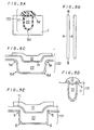
- Figs. 65 to 72 are cross-sectional views showing a conventional process for forming a trench MOS gate portion in step-by-step fashion.
- Fig. 72 is a cross-sectional view when a trench MOS gate portion 131 has been formed.
- a doped P type region 2 is initially formed on an upper surface of a semiconductor substrate 1 made of Si and the like.
- a heavily doped N type region 3 is selectively formed in an upper surface of the doped P type region 2.
- An oxide film 21 is formed on top of the structure thus obtained.
- a trench 4 is formed which extends through the oxide film 21, the doped P type region 2, and the heavily doped N type region 3 (Fig. 65).
- a silicon oxide film 7 is formed in the trench 4 (Fig. 66). After the oxide films 7 and 21 are removed (Fig. 67), a silicon oxide film is formed as a gate oxide film 9 (Fig. 68).
- the silicon oxide film 7 of 100 to 300 nm in thickness is formed in an atmosphere of oxygen at a temperature ranging from 950 to 1100 °C, for example.
- the gate oxide film 9 is generally formed by thermal oxidation in an atmosphere of steam at a temperature not more than 1000 °C. This is because the oxide film formed by thermal oxidation in an atmosphere of steam is, in general, less defective than the oxide film formed by thermal oxidation in an atmosphere of oxygen and because the oxide film is less defective at a lower temperature.
- Low-resistance polycrystalline silicon 10 for example, is filled into the trench 4 (Fig. 69) to form a gate electrode 22 in the trench 4.
- a silicon oxide film 11 is formed on the gate electrode 22 (Fig. 70).
- a CVD oxide film 12 is formed on top of the structure provided through the foregoing steps (Fig. 71) and is then shaped by etching into the trench MOS gate portion 131 (Fig. 72).
- the trench 4 after the silicon oxide film 7 is once formed and removed has a characteristic configuration as illustrated in Fig. 67. That is, an opening portion and a bottom of the trench 4 are of angular configurations 5c and 6c, respectively.
- Such configurations of the trench 4 result in a non-uniform thickness of the gate oxide film 9 formed in the trench 4.
- the gate oxide film 9 is most pronouncedly thin in positions reflecting a configuration 5d of the opening portion of the trench 4 and a configuration 6d of the bottom of the trench 4.
- Such reduced thickness of the gate oxide film 9 in the trench 4 particularly in the opening portion and bottom of the trench 4 results in gate breakdown position and breakdown voltage failures.
- a leak current of the gate oxide film 9 increases.
- the angular configurations 5c, 6c of the trench 4 deteriorate the characteristics of the trench MOS gate portion 131.
- defects are prone to occur about the trench 4.
- the defects deteriorate the characteristics of channels formed when a predetermined potential is applied to the gate electrode 22, and reduces a mobility in an MOS gate channel which is a basic characteristic of a power device having the trench MOS gate portion 131 due to defects, strain and contamination adjacent an MOS gate interface, resulting in a rise in on state voltage.
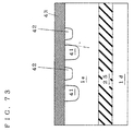
- Figs. 73 to 81 are cross-sectional views showing a process for fabricating lateral IGBTs trench-isolated in an SOI (silicon on insulator) structure in step-by-step fashion.
- substrates 1e and 1d made of silicon and the like are bonded together, with a silicon oxide film 25 therebetween.
- P layers 41 and N + layers 42 are selectively formed in an upper portion of the semiconductor substrate 1e.
- a silicon oxide film 43 is formed over the semiconductor substrate 1e.
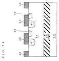
- the silicon oxide film 43 is selectively removed so that parts of the P layers 41 and N + layers 42 are exposed (Fig. 74), and silicon etching is performed using the remaining silicon oxide film 43 as a mask. This permits the semiconductor substrate 1e to be selectively excavated down to form trenches 44 (Fig. 75).
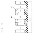
- sacrificial oxide films 45 are once selectively formed on inner walls of the trenches 44 by thermal oxidation (Fig. 76), and the silicon oxide films are etched. This permits the removal of parts of the silicon oxide film 25, all of the sacrificial oxide films 45 and all of the silicon oxide film 43, and also permits the trenches 44 to be further excavated down to the level lower than the bottom of the semiconductor substrate 1e (Fig. 77).
- Thermal oxidation in an atmosphere of steam at a temperature not more than 1000 °C provides isolation oxide films 46 around the remaining semiconductor substrate 1e (including the P layers 41 and N + layers 42) (Fig. 78).
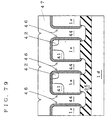
- Polycrystalline silicon 47 is deposited over the structure of Fig. 78 to fill the trenches 44 with the polycrystalline silicon 47 (Fig. 79).
- the polycrystalline silicon 47 over the semiconductor substrate 1e is selectively removed so that the polycrystalline silicon 47 remains only in the trenches 44.
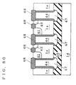
- the polycrystalline silicon 47 is covered with field oxide films 48.
- the field oxide films 48 are also formed on the surface of the semiconductor substrate 1e between the P layers 41 and the N + layers 42 (Fig. 80). Then a predetermined doped layer is formed, and lateral IGBTs are formed which are isolated from each other by isolating portions 13a having a trench structure (Fig. 81).
- the isolating portions 13a in this manner causes the problems of the thickness of the isolation oxide films 46 similar to the first background art problems.
- the semiconductor substrate 1e including the P layers 41 and N + layers 42
- the isolation oxide films 46 in these portions are pronouncedly thinner than those in other portions.
- the isolation oxide films 46 are prone to be broken particularly in the bottoms 44b. This causes the problem of a lowered isolation breakdown voltage by the isolating portions 13a.
- the present invention is intended for a method of fabricating a semiconductor device.
- the method comprises the steps of: (a) anisotropically etching a substrate made of semiconductor to form a trench extending in a direction of the thickness of the substrate; (b) performing a first thermal oxidation to form a first sacrificial oxide film in the trench; (c) removing the first sacrificial oxide film; (d) performing a second thermal oxidation to form a second sacrificial oxide film in the trench after the step (c); (e) removing the second sacrificial oxide film; (f) forming an insulating film comprising a part of a control electrode in the trench after the step (e); and (g) filling the trench to form the control electrode opposed to the substrate through the insulating film comprising the part of the control electrode.
- the opening portion and bottom of the trench are rounded by forming the first and second sacrificial oxide films to reduce the defects adjacent the trench. Since acute-angle portions are eliminated at the interface between the semiconductor substrate and the insulating film, the electric field concentration is alleviated in the edges and a uniform electric field distribution is provided.
- the second thermal oxidation is performed in a water-containing atmosphere
- the first thermal oxidation is performed in an atmosphere of oxygen at a first temperature higher than a second temperature at which the second thermal oxidation is performed.
- the bottom of the trench is mainly rounded by the water-containing oxidation.
- the second oxidation completely removes the region including defects and strains concentrated adjacent the surface of the trench by the first oxidation.
- the first temperature is not less than 1000 °C.
- the opening portion of the trench is rounded in configuration.
- the opening portion and bottom of the trench are rounded and the defects are decreased adjacent the trench, the electric field concentration is avoided, and a carrier mobility is improved. Therefore, a high-speed operation of the device is enabled.
- the method comprises the steps of: (a) anisotropically etching a substrate made of semiconductor to form a trench having an aspect ratio of from 2 to 30 and extending in a direction of the thickness of the substrate; (b) performing a thermal oxidation in an atmosphere of oxygen at a temperature not less than 1000 °C to form in the trench a sacrificial oxide film having a thickness one-tenth to three-tenths the size of an opening portion of the trench; (c) removing the sacrificial oxide film; (d) forming an insulating film comprising a part of a control electrode in the trench after the step (c); and (e) filling the trench to form the control electrode opposed to the substrate through the insulating film comprising the part of the control electrode.
- the thickness of the sacrificial oxide film By suitably controlling the thickness of the sacrificial oxide film, only one formation of the sacrificial oxide film is sufficient. This simplifies the process steps.
- the method comprises the steps of: (a) anisotropically etching a substrate made of semiconductor to form a trench extending in a direction of the thickness of the substrate; (b) performing a thermal oxidation to form a sacrificial oxide film in the trench; (c) removing the sacrificial oxide film; (d) oxidizing an inside of the trench at an atmosphere of oxygen at a temperature not less than 1000 °C to form an insulating film comprising a part of a control electrode after the step (c); and (e) filling the trench to form the control electrode opposed to the substrate through the insulating film comprising the part of the control electrode.
- the opening portion of the trench is rounded by properly adjusting the atmosphere and temperature when the insulating film comprising the part of the control electrode is formed.
- the method comprises the steps of: (a) anisotropically etching a substrate made of semiconductor to form a trench extending in a direction of the thickness of the substrate; (b) providing on the substrate a mask having an edge backing away a predetermined distance from an opening portion of the trench; (c) performing an isotropic dry etching on the substrate by using the mask; (d) oxidizing an inside of the trench in an atmosphere of steam at a temperature not more than 1000 °C after the step (c); and (e) filling the trench to form a control electrode opposed to the substrate through the insulating film comprising the part of the control electrode.
- the opening portion and bottom of the trench are rounded by the isotropic dry etching.
- the distance is 100 to 400 nm.
- the predetermined distance which is not less than 100 nm does not form the angular opening portion of the trench.
- the predetermined distance which is not more than 400 nm prevents the isotropic etching in the opening portion of the trench from proceeding more than necessary in the direction of the thickness of the substrate and in the lateral direction.
- the oxide-based film is deposited by the isotropic etching, thereby smoothing the inner wall of the trench.
- the method further comprises the steps of: (f) performing a thermal oxidation to form a sacrificial oxide film in the trench; and (g) removing the sacrificial oxide film, the steps (f) and (g) being performed after the step (c) and before the step (d).
- the sacrificial oxide film is formed and then removed, providing further rounded opening portion and bottom of the trench.
- the method comprises the steps of: (a) providing a semiconductor layer on a substrate including an insulating film at least on its surface; (b) anisotropically etching the semiconductor layer to form a trench extending in a direction of the thickness of the semiconductor layer; (c) performing a thermal oxidation to form a sacrificial oxide film in the trench; (d) removing a part of the substrate which lies under the trench and the sacrificial oxide film; (e) oxidizing an inside of the trench in an atmosphere of oxygen at a temperature not less than 1000 °C to form an isolation oxide film after the step (d); and (f) filling the trench with a burying material.
- the formation of the isolation oxide film permits the bottom of the trench to be rounded.
- the method comprises the steps of: (a) providing a semiconductor layer on a substrate including an insulating film at least on its surface; (b) anisotropically etching the semiconductor layer to form a trench extending in a direction of the thickness of the semiconductor layer; (c) removing a predetermined distance of a part of the insulating film on the substrate which lies under the trench to form a recess having a diameter greater than a diameter of the trench; (d) performing an isotropic dry etching on the semiconductor layer; (e) oxidizing an inside of the trench in an atmosphere of steam at a temperature not more than 1000 °C to form an isolation oxide film after the step (d); and (f) filling the trench with a burying material.
- the isotropic dry etching permits the bottom of the trench to be rounded.
- the predetermined distance is 100 to 400 nm.
- the predetermined distance which is not less than 100 nm does not form the angular opening portion of the trench.
- the predetermined distance which is not more than 400 nm prevents the isotropic etching in the opening portion of the trench from proceeding more than necessary in the direction of the thickness of the substrate and in the lateral direction.
- the oxide-based film is deposited by the isotropic etching, thereby smoothing the inner wall of the trench.
- the method further comprises the steps of: (g) performing a thermal oxidation to form a sacrificial oxide film in the trench; and (h) removing the sacrificial oxide film, the steps (g) and (h) being performed after the step (d) and before the step (e).
- the sacrificial oxide film is formed and then removed, providing further rounded bottom of the trench.
- the method comprises the steps of: (a) providing a semiconductor layer on a substrate including an insulating film at least on its surface; (b) anisotropically etching the semiconductor layer to form a trench extending in a direction of the thickness of the semiconductor layer; (c) performing a thermal oxidation to form a sacrificial oxide film in the trench; (d) removing a part of the substrate which lies under the trench and the sacrificial oxide film; (e) forming a polycrystalline semiconductor layer on an inner wall of the trench; (f) oxidizing the polycrystalline semiconductor layer to form an isolation oxide film; and (g) filling the trench with a burying material.
- the polycrystalline semiconductor layer covers the corners of the semiconductor layer in the bottom of the trench with good coverage.
- the polycrystalline semiconductor layer is oxidized to provide the isolation oxide film which permits the bottom of the trench to be rounded.
- the method comprises the steps of: (a) providing a semiconductor layer on a substrate including a semiconductor oxide film; (b) anisotropically etching the semiconductor layer to form a trench having an aspect ratio of from 2 to 30 and extending in a direction of the thickness of the semiconductor layer; (c) performing a thermal oxidation in an atmosphere of oxygen at a temperature not less than 1000 °C to form in the trench a sacrificial oxide film having a thickness one-tenth to three-tenths the size of an opening portion of the trench; (d) removing the sacrificial oxide film; (e) forming an isolation oxide film in the trench after the step (c); and (f) filling the trench with a burying material.
- the first fabrication method is a method of fabricating a gate oxide film in a trench which is different from the background art method.
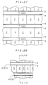
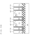
- Figs. 1 to 5 are cross-sectional views showing a method of forming a trench MOS gate portion 132 in step-by-step fashion according to a first preferred embodiment of the present invention.
- An oxide film 21 is formed on a substrate 1 made of silicon.
- An opening is selectively formed in the oxide film 21, and anisotropic silicon etching is performed using the oxide film 21 as a mask to form a trench 4 extending in a direction of the thickness of the substrate 1 (Fig. 1).
- an opening portion and a bottom of the trench 4 are of angular configurations 5 and 6, respectively.
- a sacrificial oxide film 7 of about 100 to 300 nm in thickness is formed in an atmosphere of oxygen at a temperature ranging from 950 to 1100 °C, for example, (Fig. 2) and is then removed (Fig. 3).
- Fig. 2 a temperature ranging from 950 to 1100 °C, for example
- thermal oxidation in an atmosphere of oxygen at a temperature not less than 1000 °C (for example, 1215 °C) provides a gate oxide film 9 (Fig. 4).
- An oxide film formed by thermal oxidation in an atmosphere of oxygen is more effective in rounding the opening portion 5e of the trench 4 than an oxide film formed by thermal oxidation in an atmosphere of steam when it is formed on an inner wall of the trench after a sacrificial oxide film is formed and then removed.
- the trench MOS gate portion 132 is formed (Fig. 5A).
- Fig. 5A is a cross-sectional view taken along the line A-A of Fig. 5B.
- Fig. 5B is a plan view illustrating the vicinity of the trench MOS gate portion 132.
- Fig. 5C is a cross-sectional view taken along the line B-B of Fig. 5B.
- the plan view of the vicinity of the trench MOS gate portion 131 is also shown in Fig. 5B, but the sections thereof taken along the lines A-A and B-B are shown in Figs. 5D and 5E, respectively.
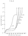
- Fig. 6 is a graph illustrating the relation (leak characteristic) between an applied voltage Vg and a leak current Ig when a simple capacitance structure including no diffused layer is formed adjacent the trench.
- the curve G 131 represents the characteristic of the background art trench MOS gate portion 131 shown in Figs. 5D and 5E wherein the trench has the angular opening portion and bottom
- the curve G 132 represents the characteristic of the trench MOS gate portion 132 shown in Figs. 5A and 5C to which the present invention is applied.
- the voltage Vg is applied between the substrate 1 and a gate electrode 22.
- the trench MOS gate portion 131 of Fig. 72 is measured when the doped P type region 2 and the heavily doped N type region 3 are not formed on the substrate 1.
- the gate oxide films of the trench MOS gate portions 131, 132 are designed to be about 750 angstroms in thickness.
- the leak characteristic of the trench MOS gate portion 131 abruptly deteriorates when the applied voltage Vg substantially exceeds 30 V. It will be understood that the isolation breakdown voltage for the trench MOS gate portion 131 is about 55 V.
- the leak characteristic of the trench MOS gate portion 132 does not substantially deteriorate when the applied voltage exceeds 40 V, and the isolation breakdown voltage for the trench MOS gate portion 132 is more than 60 V.
- the improved configuration of the trench 4 permits the trench MOS gate portion 132 to have the improved leak characteristic and improved isolation breakdown voltage over the trench MOS gate portion 131 of the first background art.
- the second fabrication method is a technique for smoothing the trench configuration by isotropic plasma etching.
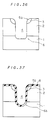
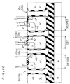
- Figs. 7 to 14 are cross-sectional views showing a method of forming a trench MOS gate portion 133 in step-by-step fashion according to a second preferred embodiment of the present invention associated with claims 6 to 9.
- the structure shown in Fig. 1 is formed in the same manner as the first preferred embodiment.
- the opening portion and bottom of the trench 4 are of angular configurations 5 and 6, respectively.
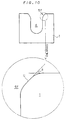
- the oxide film 21 is removed selectively in a portion adjacent the opening of the trench 4 so that the oxide film 21 backs away a distance x from the trench 4 (Fig. 7). Then isotropic plasma etching is performed on silicon using an O 2 / CF 4 based gas. The result is a chamfered opening portion of the trench 4 and a rounded bottom configuration 6e thereof having no angular portions. At this time, an oxide-based film 91 is produced adjacent the bottom of the trench 4 as will be described later in detail (Fig. 8).
- the sacrificial oxide film 7 is once formed (Fig. 9) and is then removed, thereby providing a more smoothed configuration 5f of the opening portion of the trench 4 (Fig. 10).
- the configuration 5f sometimes has a linear portion U.
- the linear portion U and the upper surface of the substrate 1 form an angle ⁇ which falls within the range of 30 to 60 degrees.
- a tangent line drawn from a portion of the configuration 5f which has the smallest radius of curvature and the upper surface of the substrate 1 form an angle ⁇ which falls within the range of 30 to 60 degrees.
- the gate oxide film 9 is formed by thermal oxidation in an atmosphere of steam at a temperature not more than 1000 °C (for example, 950 °C) (Fig. 11).
- the thermal oxidation is performed in the atmosphere of oxygen at the temperature not less than 1000 °C for the purpose of forming the gate oxide film 9.
- thermal oxidation in the atmosphere of steam at the temperature not more than 1000 °C provides better characteristics. The reasons therefor is not evident at the present time.
- the trench 4 is filled with low-resistance polycrystalline silicon and the gate electrode 22 is formed.
- a silicon oxide film 11 is formed on the gate electrode, and an oxide film 12 is deposited over the top surface by the CVD process, for example. Further, the gate oxide film 9 and the oxide film 12 are selectively left by etching to form the trench MOS gate portion 133 (Fig. 12).
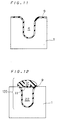
- the gate electrode 22 may extend to a higher level than the upper surface of the substrate 1 as shown in Figs. 13 and 14.
- metal films W, Mo, Al, Ti
- metallic compounds WSi, MoSi 2 , AlSi, TiSi
- the leak characteristic of the trench MOS gate portion 133 formed in this manner is represented as the curve G 133 of Fig. 6.
- the leak characteristic of the trench MOS gate portion 133 is about an order of magnitude less than that of the trench MOS gate portion 132 of the first preferred embodiment when the applied voltage Vg is low (not more than 40 V), but is greater when the applied voltage Vg is high (not less than 50 V). That is, when the present invention is applied to a device having a main breakdown voltage which is less than the isolation breakdown voltage of the gate oxide film, the trench MOS gate portion 132 is more suitable than the trench MOS gate portion 133. Conversely, when the present invention is applied to a device having a main breakdown voltage which is more than the isolation breakdown voltage of the gate oxide film, the trench MOS gate portion 133 is more suitable than the trench MOS gate portion 132.
- the leak characteristic of the resultant trench MOS gate portion is substantially equal to or less than that of the trench MOS gate portion 132 when the applied voltage Vg is high (not less than 50 V).
- the distance x backed away by the oxide film 21 from the opening portion of the trench 4 is preferably not less than 100 nm and not more than 400 nm.
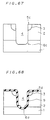
- Figs. 15 and 16 are cross-sectional views on an enlarged scale illustrating the opening portion of the trench 4 after the isotropic plasma etching when the distance x is less than 100 nm and when the distance x is greater than 400 nm, respectively.
- the broken lines of Figs. 15 and 16 indicate the configuration of the substrate 1 before the isotropic plasma etching.
- the opening portion of the trench 4 has an angular edge 51.
- the etching proceeds in the direction of the thickness of the substrate 1, and the opening portion of the trench 4 directly reflects the configuration of the oxide film 21 and is not chamfered. Therefore the distance x preferably ranges from 100 nm to 400 nm.
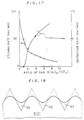
- Fig. 17 is a graph illustrating how a silicon etching rate and a deposition rate of the oxide-based film vary as the ratio R of the gas varies. The graph shows that, as the ratio R of the gas increases, the etching rate decreases and the deposition rate of the film increases.
- Fig. 18 is a schematic cross-sectional view of an etched surface of silicon (for example, the substrate 1) in exaggeration when R is greater than 1.
- the broken lines of Fig. 18 indicate the configuration of the silicon before etching.
- the deposition of an oxide-based film 92 permits recesses to be filled, and etching eliminates projections. As a result, the configuration of the etched surface is considered to be smoothed.
- the silicon etching rate is generally equal to the deposition rate of the oxide-based film.
- the substantial etching rate is not more than 15 nm/min. and it takes tens of minutes for 200 to 300 nm etching required to chamfer the opening portion of the trench 4. This significantly reduces the productivity and makes it difficult to control the sample temperatures during etching, which is not practical.
- the ratio R is preferably less than 5.
- the film deposition simultaneous with the silicon etching allows the inner wall of the trench 4 to be smoothed, and the breakdown voltage of the trench MOS gate portion 133 is considered to increase.
- Fig. 19 is a graph illustrating how the breakdown voltage of the trench MOS gate portion 133 varies with variation in the ratio R of the gas.
- the breakdown voltage is actually measured when R is not more than 3 but is not measured when R is more than 3.
- the upper branch L1 of the graph indicates a breakdown voltage expected from the deposition rate of the oxide-based film
- the lower branch L2 is a breakdown voltage expected from the etching rate.
- a breakdown voltage in a region between the branches L1 and L2 is expected to be obtained in practice.
- a leak characteristic of a trench MOS gate portion 134 formed in this case is represented by the curve G 134 of Fig. 6.
- the leak characteristic of the trench MOS gate portion 134 is less than that of the trench MOS gate portion 133 while the trench MOS gate portion 134 provides a lower leak current and a higher breakdown voltage than the trench MOS gate portion 131. This is considered to result from the fact that the configuration of the opening portion of the trench is further rounded by the step of forming and removing the sacrificial oxide film 7.
- a large displacement current generated at the gate during the turn-on and turn-off operations requires the increase in gate breakdown voltage, and the application of the second preferred embodiment is preferable.
- the leak current Ig is less than about 10 -8 A, there is a small difference in leak characteristic between the trench MOS gate portions 133 and 134.
- the trench MOS gate portion 134 requiring fewer process steps is more advantageous than the trench MOS gate portion 133 in terms of cost versus actual performance.
- the second and third preferred embodiments may be used and applied depending on the purposes of devices to be applied.
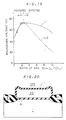
- Fig. 6 there is also shown a curve G 135 indicative of the leak characteristic of an MOS gate structure 135 of the type parallel to the surface of the substrate 1 for the purpose of comparison.
- Fig. 20 is a cross-sectional view illustrating the MOS gate structure 135.
- the gate oxide film 9 surrounded by an isolation oxide film F is formed on the substrate 1, and the gate electrode 22 is formed on the gate oxide film 9.
- the gate electrode 22 is covered with the silicon oxide film 11.
- the gate oxide film 9 is formed by thermal oxidation in an atmosphere of steam at a temperature not more than 1000 °C, like the second preferred embodiment.
- the voltage Vg is applied between the substrate 1 and the gate electrode 22.
- trench MOS gate portions 132, 133, 134 provide desirable characteristics which are somewhat inferior to but close to the characteristics of the MOS gate structure 135.
- the trench MOS gate portions 132, 133, 134 of the first to third preferred embodiments may be applied to various vertical power devices.
- Fig. 21 is a cross-sectional view of a trench gate type MOSFET 100.
- a doped P type region 2 is formed on the N type semiconductor substrate 1, and a heavily doped N type region 3 is formed selectively in an upper surface of the doped P type region 2.
- a trench extends through the doped P type region 2 and heavily doped N type region 3 into the N type semiconductor substrate 1 to form a trench MOS gate portion 13.
- Source electrodes 14a are formed on the doped P type region 2 and in contact with the heavily doped N type region 3.
- a drain electrode 14c is formed in contact with the N type semiconductor substrate 1. The present invention may be applied to this trench MOS gate portion 13 to improve the leak characteristic.
- Fig. 22 is a cross-sectional view of another trench gate type MOSFET 200.
- the trench gate type MOSFET 200 comprises an N + layer 1b between the drain electrode 14c and the N type semiconductor substrate 1.
- the present invention may be also applied to such a device.
- the trench gate MOSFETs represent an improvement over the conventional MOSFETs in that a higher degree of integration decreases an on-state resistance.
- the application of the trench MOS gate portion forming method of the present invention to such power devices has the effect of improving the gate breakdown voltage because of suppressed electric field concentration adjacent the gate electrode 22.
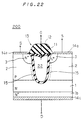
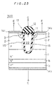
- Fig. 23 is a cross-sectional view of a trench gate type IGBT (insulated gate bipolar transistor) 300.
- the trench gate type IGBT 300 comprises a P + layer 1c formed on a lower surface (a surface on which the N type semiconductor substrate 1 is not formed) of the N + layer 1b of the trench gate type MOSFET 200.
- a collector electrode 14b is formed in contact with the P + layer 1c.
- the source electrodes 14a for the trench gate type MOSFET 200 function as an emitter electrode for the trench gate type IGBT 300.
- a channel region 15 is formed in the doped P type region 2 around the gate oxide film 9 by the application of a predetermined potential to the gate electrode 22.
- Figs. 24 to 27 are plan views showing the top structures of the trench gate type IGBTs and trench gate type MOSFETs.
- the trench gate type MOSFETs 100, 200 and the trench gate type IGBT 300 may be constructed as shown in the plan views of Figs. 24 to 27.
- the top structures shown in Figs. 26 and 27 have some differences in cross-section from the structures shown in Figs. 22 and 23.
- Fig. 28 illustrates a part of Fig. 26.
- Figs. 29 and 30 are cross-sectional views taken along the lines A-A and B-B of Fig. 28.
- Figs. 29 and 30 differ in construction from Fig. 22.
- Fig. 31 is a cross-sectional view of a lateral trench gate type MOSFET 400 having the trench MOS gate portion 13.
- the lateral trench gate type MOSFET 400 differs from the trench gate type MOSFET 200 of Fig. 22 in that the N + layer 1b and the drain electrode 14c are not formed and that one of the electrodes 14a serves as a source electrode and the other as a drain electrode.
- Fig. 32 is a cross-sectional view of a trench type MCT (MOS controlled thyristor) 500.
- the fabrication method of the first to third preferred embodiments may be applied to the trench MOS gate portions 13 of these devices. Since the damages to and contamination on the inner wall of the trench 4 which are produced by anisotropic etching are removed, the carrier mobility in the channel is improved. This reduces the channel resistance in the on state to reduce the on-state resistance of the whole device.
- Fig. 33 is a cross-sectional view of a trench type diode 600.
- a positive potential is not applied to the gate electrode 22 in the on state but a negative potential is applied thereto in the off state.
- the use of the trench MOS gate portion 13 formed by the fabrication method of the first to third preferred embodiments avoids the electric field concentration.
- the third fabrication method is a technique for forming the sacrificial oxide film twice.
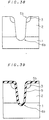
- Figs. 34 to 43 are cross-sectional views showing a process for forming a trench MOS gate portion in step-by-step fashion according to a fourth preferred embodiment of the present invention.
- the doped P type region 2 and the heavily doped N type region 3 are formed on the substrate 1, and the oxide film 21 is formed on top of the regions 2 and 3 in the same manner as the background art.
- An opening is cut selectively in the oxide film 21 on the heavily doped N type region 3.
- the trench 4 extending through the doped P type region 2 and the heavily doped N type region 3 is formed by anisotropic etching (Fig. 34). At this point of time, the opening portion and bottom of the trench 4 are of angular configurations 5 and 6, respectively.
- the silicon oxide film 7 is formed in the trench 4 in an atmosphere of oxygen at a relatively high temperature T H .
- the temperature T H is not less than 1000 °C, for example 1100 °C.
- the atmosphere used herein is, for example, an atmosphere of 100 % oxygen. Since a soft oxide film is formed at an temperature of 1000 °C or more, the opening portion of the trench 4 has a rounded configuration as designated at 5g.
- the silicon oxide films 7 and 21 are removed by etching (Fig. 36).
- a silicon oxide film 8 is formed in the trench 4 in an atmosphere of steam (Fig. 37). Formation of the silicon oxide film 8 under such conditions provides a rounded configuration 6b of the bottom of the trench 4 and a further rounded configuration 5b of the opening portion of the trench 4.
- a temperature T L used at this time is lower than the temperature T H and is, for example, 950 °C.
- the thickness of the silicon oxide films 7, 8 may be selected to be on the order of one-twentieth to one-fifth the opening size. That is, the thickness of the silicon oxide films 7, 8 to be formed relative to the trench 4 of 1 ⁇ m in width is selected to be on the order of 50 to 200 nm, for example 100 nm.
- the silicon oxide film 8 is removed by etching.
- the two processes of forming and removing the silicon oxide films 7, 8 under the above-mentioned conditions allow the trench 4 to have the opening portion and bottom of rounded configurations as designated at 5b and 6b.
- a silicon oxide film is formed in the trench 4 as the gate oxide film 9 (Fig. 39).
- the rounded configurations of the opening portion and bottom of the trench 4 prevent a phenomenon in which the gate oxide film 9 is partially thin as having occurred in the background art and allow the gate oxide film 9 to be formed uniformly in the trench 4.
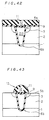
- low-resistance polycrystalline silicon 10 is deposited on top of the structure provided through the foregoing steps, and the trench 4 is filled with the low-resistance polycrystalline silicon 10 through the gate oxide film 9 (Fig. 40).
- the low-resistance polycrystalline silicon 10 is selectively left by etching technique to form the gate electrode 22 made of the low-resistance polycrystalline silicon 10 in the trench 4.
- the silicon oxide film 11 is formed on the gate electrode 22 (Fig. 41), and the oxide film 12 is deposited over the top surface by CVD process, for example (Fig. 42).
- the oxide film 12 is selectively left by etching to form the trench MOS gate portion 13 (Fig. 43).
- the defects subjected to the gettering effect into the vicinity of the inner wall of the trench 4 are drawn into the silicon oxide film 8.
- the defects of the semiconductor about the trench 4 are reduced as compared with the background art.
- the defect reduction can improve the mobility of carriers in channels to be formed in the semiconductor about the trench 4 when a predetermined potential is applied to the gate electrode 22.
- the on-state voltage is improved by applying the fabrication method of the fourth preferred embodiment to the formation of the trench MOS gate portion 13 of the trench gate type IGBT 300 of Fig. 23.
- Fig. 44 illustrates an on state voltage which is a basic characteristic of the trench gate type IGBT.
- the on state voltage of the trench gate type IGBT 100 is provided by the application of the present invention, and it is 1.44 V.
- the on state voltage of the trench gate type IGBT having the trench MOS gate portion is provided by interchanging the first and second sacrificial oxidation conditions, and it is 1.63 V.
- the on state voltage of the trench gate type IGBT having the trench MOS gate portion is provided by the conventional fabrication method, and it is 1.64 V. It should be noted that a turn-off time is constant (200 ns) under the respective conditions.
- the method of forming the trench MOS gate portion of the fourth preferred embodiment can reduce the on-state voltage of the trench gate type IGBT. This significantly improves power loss.
- the trench 4 has the rounded configuration, and contamination of the substrate 1 on the trench inner wall, defects adjacent the trench, and residual stress are reduced. This improves the interface state and carrier mobility in the channel regions 15 to enhance the characteristics of the trench MOS gate. The result is a reduction in on state voltage which is a basic characteristics of power devices, an improved switching characteristic and, accordingly, a reduction in power loss.
- the fabrication method of the fourth preferred embodiment may be applied to the trench gate type MOSFETs 100, 200 of Figs. 21, 22, the lateral trench gate type MOSFET 400 of Fig. 31, and the trench type MCT 500 of Fig. 32.
- the application of the fourth preferred embodiment to such power devices represents an improvement which is an increased electron mobility in the channel region 15.
- the fourth preferred embodiment may be also applied to the trench type diode 600 of Fig. 33.
- the thickness of the silicon oxide film 7 formed by the first sacrificial oxidation is selected to be on the order of one-twentieth to one-fifth the opening size of the trench 4 in the fourth preferred embodiment. Selection of the thickness which is not less than one-tenth the opening size affords a further rounded configuration of the opening portion of the trench 4 to improve the breakdown voltage of the gate oxide film 9 without the second sacrificial oxidation and silicon oxide film 8. Thus, the process steps are simplified.
- the thickness of the silicon oxide film 7 is selected to be not more than three-tenths the opening size of the trench 4 so that the trench 4 is filled up and the bottom of the trench 4 is not warped.
- the semiconductor substrate 1 may be made up of a semiconductor compound such as SiC x (0 ⁇ x ⁇ 1), SiGe y (0 ⁇ y ⁇ 1) or the like, thereby providing further advantages.
- the substrate When SiC x is used as a substrate, the substrate may be used at a high temperature because of its great band gap, and a device for a high breakdown voltage is reduced in thickness.
- the use of SiGe y permits a high-speed operation of the device because of its small band gap and great mobility.
- the fourth fabrication method is a technique for trench isolation in the SOI structure.
- a sixth preferred embodiment provides a technique for forming an oxide film on the trench inner wall in an atmosphere of oxygen at a temperature not less than 1000 °C, like the first preferred embodiment.
- substrates 1e and 1d made of silicon and the like are bonded together, with a silicon oxide film 25 therebetween.
- P layers 41 and N + layers 42 are selectively formed in an upper portion of the semiconductor substrate 1e.
- a silicon oxide film 43 is formed over the semiconductor substrate 1e (Fig. 73).
- the silicon oxide film 43 is selectively removed so that parts of the P layers 41 and N + layers 42 are exposed (Fig. 74), and silicon etching is performed using the remaining silicon oxide film 43 as a mask. This permits the semiconductor substrate 1e to be selectively excavated down to form trenches 44 (Fig. 75).
- sacrificial oxide films 45 are once formed on inner walls of the trenches 44 by thermal oxidation (Fig. 76), and the silicon oxide films are etched. This permits the removal of parts of the silicon oxide film 25, all of the sacrificial oxide films 45 and all of the silicon oxide film 43, and also permits the trenches 44 to be further excavated down to the level lower than the bottom of the semiconductor substrate 1e (Fig. 77).
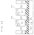
- Fig. 45 is a cross-sectional view of the structure provided in the above described process steps in the sixth preferred embodiment.
- the corners of the semiconductor substrate 1e are rounded by the formation of the isolation oxide films 46 like the first preferred embodiment.
- bottoms 44c of the trenches 44 are more rounded than the bottoms 44b of Fig. 78.
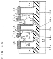
- Fig. 46 is a cross-sectional view of the lateral IGBTs fabricated in this manner.
- isolating portions 13b having a trench structure include the isolation oxide films 46 which are not locally thin as compared with the isolating portions 13a of the second background art. This solves the problem of the decrease in isolation breakdown voltage.
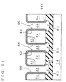
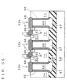
- Figs. 47 to 55 are cross-sectional views illustrating a method of fabricating a semiconductor device in step-by-step fashion according to a seventh preferred embodiment of the present invention.
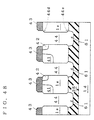
- Fig. 75 The structure of Fig. 75 is initially obtained in the same manner as the second background art. Isotropic etching is performed on the silicon oxide films to laterally etch and back away the silicon oxide films 43 serving as a trench etching mask and to form recesses 61 in the silicon oxide film 25 under the trenches 44. The corners of the substrate 1e are exposed a distance x in the recesses 61 (Fig. 47).
- isotropic silicon etching is performed to round the corners of the substrate 1e exposed in the recesses 61 and chamfer bottoms 44e of the trenches 44.
- the oxide-based films deposited by the isotropic silicon etching are removed (Fig. 48).
- the distance x is preferably 100 to 400 nm.
- the etching gas is an O 2 / CF 4 based gas, and the ratio R preferably satisfies 1 ⁇ R ⁇ 5.
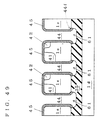
- the sacrificial oxide films 45 are once formed on the inner walls of the trenches 44 by thermal oxidation (Fig. 49), and the silicon oxide films are etched. This permits the removal of all of the sacrificial oxide films 45 and silicon oxide film 43 and also permits bottoms 44f of the trenches 44 to be further rounded (Fig. 50).
- Thermal oxidation in an atmosphere of steam at a temperature not more than 1000 °C provides the isolation oxide films 46 around the remaining semiconductor substrate 1e (including the P layers 41 and N + layers 42) (Fig. 51).
- the polycrystalline silicon 47 is deposited over the structure of Fig. 51 to fill the trenches 44 (including the recesses 61) with the polycrystalline silicon 47 (Fig. 52).
- the polycrystalline silicon 47 over the semiconductor substrate 1e is selectively removed so that the polycrystalline silicon 47 remains only in the trenches 44 (Fig. 53).
- the polycrystalline silicon 47 is covered with the field oxide films 48.
- the field oxide films 48 are also formed on the surface of the semiconductor substrate 1e between the P layers 41 and the N + layers 42 (Fig. 54). Then a predetermined doped layer is formed, and the lateral IGBTs are formed which are isolated from each other by isolating portions 13c having a trench structure (Fig. 55).
- the isolation oxide films 46 are not locally thin. This solves the problem of the decrease in isolation breakdown voltage.
- the silicon oxide film 43 may back away a distance y from the opening portion of the trenches 44. If the silicon oxide film 43 is sufficiently thick relative to the distance x, the silicon oxide film 43 need not be covered with a resist. As a result, since the distance y is generally equal to the distance x if the P layers 41 and the N + layers 42 are exposed the distance y around the trenches 44, opening portions 44d of the trenches 44 are also rounded by the isotropic silicon etching. This is a secondary preferable effect of the present invention. However, the opening portions 44d are subsequently covered with the filed oxide films 48, and the effect of the present invention is not prevented.
- the isolation oxide films 46 are prevented from becoming locally thin as compared with the second background art since the bottoms 44e of the trenches 44 are chamfered if the process steps of forming and removing the sacrificial oxide films 45 like the third preferred embodiment.
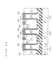
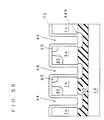
- Figs. 56 to 61 are cross-sectional views illustrating a method of fabricating a semiconductor device in step-by-step fashion according to an eighth preferred embodiment of the present invention.
- Fig. 77 The structure of Fig. 77 is initially obtained in the same manner as the second background art.
- the silicon oxide film 25 is etched to a depth of about 200 to 300 nm, for example, to form the extending trenches 44.
- Polycrystalline silicon 71 is deposited to a thickness of 200 to 300 nm over the top surface. Then, the polycrystalline silicon 71 is exposed on the inner surfaces of the trenches 44 (Fig. 56).
- polycrystalline silicon has a good step coverage and covers the corners of the trenches 44 if the corners of the substrate 1e are projecting in the bottoms 44b of the trenches 44.
- the silicon oxide film 72 serving as an isolation oxide film has a thickness of 200 to 300 nm and is not locally thin.
- the polycrystalline silicon 47 is deposited in the same manner as the second background art and the seventh preferred embodiment to fill the trenches 44 with the polycrystalline silicon 47 (Fig. 58).
- the polycrystalline silicon 47 over the semiconductor substrate 1e is selectively removed so that the polycrystalline silicon 47 remains only in the trenches 44 (Fig. 59).
- the polycrystalline silicon 47 is covered with the field oxide films 48 (Fig. 60).
- a predetermined doped layer is formed, and the lateral IGBTs are formed which are isolated from each other by isolating portions 13d having a trench structure (Fig. 61).
- the isolating portions 13b, 13c, 13d are used for isolation of the lateral IGBTs from each other in the sixth to eighth preferred embodiments.
- the sixth to eighth preferred embodiments may be applied to the isolation of different devices from each other.
- Fig. 62 is a cross-sectional view of a lateral diode, a lateral IGBT, and an MOSFET isolated from each other, and illustrates the application of the sixth and seventh preferred embodiments.
- the substrate 1e is rounded in the bottoms of the isolating portions. In these portions, the silicon oxide film is not locally thin.
- Fig. 63 is a cross-sectional view of a lateral IGBT 700 in a high-voltage power IC which is provided by applying the trench formation process of the fourth preferred embodiment to trench isolation.
- the lateral IGBT 700 is formed in the semiconductor substrate 1e.
- the semiconductor substrate 1e is formed immediately over the silicon oxide film 25 formed on the semiconductor substrate 1d.
- Isolating portions 13e are formed by filling the polycrystalline silicon 10 after silicon oxide films 9a are formed. It should be noted that the polycrystalline silicon 10 does not function as a gate but the isolating portions 13e are used for isolation between devices.
- All of the isolating portions 13e may be filled with the silicon oxide films 9a and the polycrystalline silicon 10 need not be used when the isolating portions 13e have a small width (for example, 1 ⁇ m or less) or when the isolating portions 13e are wide but a thick CVD silicon oxide film is formed for a short time (for example, several hours). Further, another film (for example, silicon nitride film) may be substituted for the polycrystalline silicon 10.
- Formation of the isolating portions 13e by using the trench formation process of the fourth preferred embodiment is advantageous in that leakage is reduced in the isolating portions.
- Fig. 64 is a cross-sectional view of a lateral diode, a lateral IGBT, and an MOSFET isolated from each other in the same manner as in Fig. 62, and illustrates the application of the ninth preferred embodiment.
Landscapes
- Element Separation (AREA)
- Insulated Gate Type Field-Effect Transistor (AREA)
- Thyristors (AREA)
- Thin Film Transistor (AREA)
- Formation Of Insulating Films (AREA)
- Electrodes Of Semiconductors (AREA)
Applications Claiming Priority (5)
| Application Number | Priority Date | Filing Date | Title |
|---|---|---|---|
| JP1255994 | 1994-02-04 | ||
| JP1255994 | 1994-02-04 | ||
| JP00134795A JP3396553B2 (ja) | 1994-02-04 | 1995-01-09 | 半導体装置の製造方法及び半導体装置 |
| JP134795 | 1995-01-09 | ||
| EP95101591A EP0666590B1 (fr) | 1994-02-04 | 1995-02-06 | Méthode pour la fabrication de sillons dans un dispositif semi-conducteur |
Related Parent Applications (2)
| Application Number | Title | Priority Date | Filing Date |
|---|---|---|---|
| EP95101591.6 Division | 1995-02-06 | ||
| EP95101591A Division EP0666590B1 (fr) | 1994-02-04 | 1995-02-06 | Méthode pour la fabrication de sillons dans un dispositif semi-conducteur |
Publications (3)
| Publication Number | Publication Date |
|---|---|
| EP1160872A2 true EP1160872A2 (fr) | 2001-12-05 |
| EP1160872A3 EP1160872A3 (fr) | 2007-06-20 |
| EP1160872B1 EP1160872B1 (fr) | 2010-10-20 |
Family
ID=26334557
Family Applications (3)
| Application Number | Title | Priority Date | Filing Date |
|---|---|---|---|
| EP95101591A Expired - Lifetime EP0666590B1 (fr) | 1994-02-04 | 1995-02-06 | Méthode pour la fabrication de sillons dans un dispositif semi-conducteur |
| EP01121360A Expired - Lifetime EP1160852B1 (fr) | 1994-02-04 | 1995-02-06 | Procédé de fabrication d'un dispositif semiconducteur avec une tranchée |
| EP01121361A Expired - Lifetime EP1160872B1 (fr) | 1994-02-04 | 1995-02-06 | Dispositif semiconducteur avec une tranchée |
Family Applications Before (2)
| Application Number | Title | Priority Date | Filing Date |
|---|---|---|---|
| EP95101591A Expired - Lifetime EP0666590B1 (fr) | 1994-02-04 | 1995-02-06 | Méthode pour la fabrication de sillons dans un dispositif semi-conducteur |
| EP01121360A Expired - Lifetime EP1160852B1 (fr) | 1994-02-04 | 1995-02-06 | Procédé de fabrication d'un dispositif semiconducteur avec une tranchée |
Country Status (5)
| Country | Link |
|---|---|
| US (4) | US5783491A (fr) |
| EP (3) | EP0666590B1 (fr) |
| JP (1) | JP3396553B2 (fr) |
| KR (1) | KR100188823B1 (fr) |
| DE (3) | DE69536116D1 (fr) |
Cited By (1)
| Publication number | Priority date | Publication date | Assignee | Title |
|---|---|---|---|---|
| US9805954B2 (en) | 2011-07-21 | 2017-10-31 | Semiconductor Energy Laboratory Co., Ltd. | Semiconductor device and manufacturing method thereof |
Families Citing this family (100)
| Publication number | Priority date | Publication date | Assignee | Title |
|---|---|---|---|---|
| JP3396553B2 (ja) | 1994-02-04 | 2003-04-14 | 三菱電機株式会社 | 半導体装置の製造方法及び半導体装置 |
| FR2739493B1 (fr) * | 1995-09-29 | 2000-07-28 | Nippon Denso Co | Mosfet de puissance et son procede de fabrication |
| US6107661A (en) * | 1995-09-29 | 2000-08-22 | Nippondenso Co., Ltd. | Semiconductor device and method of manufacturing same |
| US5719085A (en) * | 1995-09-29 | 1998-02-17 | Intel Corporation | Shallow trench isolation technique |
| WO1998012741A1 (fr) * | 1996-09-18 | 1998-03-26 | Advanced Micro Devices, Inc. | Transistor vmos non auto-aligne a effet de champ, a canal court |
| JP3342412B2 (ja) | 1997-08-08 | 2002-11-11 | 三洋電機株式会社 | 半導体装置およびその製造方法 |
| JP3502531B2 (ja) * | 1997-08-28 | 2004-03-02 | 株式会社ルネサステクノロジ | 半導体装置の製造方法 |
| US6429481B1 (en) | 1997-11-14 | 2002-08-06 | Fairchild Semiconductor Corporation | Field effect transistor and method of its manufacture |
| DE19860962B4 (de) * | 1998-03-05 | 2007-02-01 | Mitsubishi Denki K.K. | Halbleitervorrichtung und Herstellungsverfahren der Halbleitervorrichtung |
| JP3705919B2 (ja) | 1998-03-05 | 2005-10-12 | 三菱電機株式会社 | 半導体装置及びその製造方法 |
| US6372599B1 (en) * | 1999-01-14 | 2002-04-16 | Mitsubishi Denki Kabushiki Kaisha | Semiconductor device and method of manufacturing the same |
| US6706604B2 (en) * | 1999-03-25 | 2004-03-16 | Hitachi, Ltd. | Method of manufacturing a trench MOS gate device |
| JP2000332242A (ja) | 1999-05-21 | 2000-11-30 | Mitsubishi Electric Corp | 半導体装置及びその製造方法 |
| KR100333378B1 (ko) * | 1999-06-23 | 2002-04-18 | 박종섭 | 반도체 소자의 제조방법 |
| DE19935442C1 (de) * | 1999-07-28 | 2000-12-21 | Siemens Ag | Verfahren zum Herstellen eines Trench-MOS-Leistungstransistors |
| JP2001085677A (ja) | 1999-09-09 | 2001-03-30 | Mitsubishi Electric Corp | 半導体装置の製造方法 |
| JP2001085686A (ja) | 1999-09-13 | 2001-03-30 | Mitsubishi Electric Corp | 半導体装置及びその製造方法 |
| AU7478400A (en) * | 1999-09-14 | 2001-04-17 | General Semiconductor, Inc. | Trench dmos transistor having improved trench structure |
| TW442972B (en) * | 1999-10-01 | 2001-06-23 | Anpec Electronics Corp | Fabricating method of trench-type gate power metal oxide semiconductor field effect transistor |
| EP1091413A3 (fr) * | 1999-10-06 | 2005-01-12 | Lsi Logic Corporation | CMOSFET à déplétion et inversion complète à canal vertical et à double grille |
| JP4860022B2 (ja) * | 2000-01-25 | 2012-01-25 | エルピーダメモリ株式会社 | 半導体集積回路装置の製造方法 |
| JP4200626B2 (ja) * | 2000-02-28 | 2008-12-24 | 株式会社デンソー | 絶縁ゲート型パワー素子の製造方法 |
| US6417554B1 (en) * | 2000-04-27 | 2002-07-09 | International Rectifier Corporation | Latch free IGBT with schottky gate |
| JP2001326273A (ja) | 2000-05-16 | 2001-11-22 | Denso Corp | 半導体装置の製造方法 |
| JP3728177B2 (ja) * | 2000-05-24 | 2005-12-21 | キヤノン株式会社 | 音声処理システム、装置、方法及び記憶媒体 |
| JP2001351895A (ja) | 2000-06-09 | 2001-12-21 | Denso Corp | 半導体装置の製造方法 |
| US6437386B1 (en) * | 2000-08-16 | 2002-08-20 | Fairchild Semiconductor Corporation | Method for creating thick oxide on the bottom surface of a trench structure in silicon |
| JP2002190595A (ja) * | 2000-12-21 | 2002-07-05 | Denso Corp | 半導体装置及びその製造方法 |
| JP4852792B2 (ja) * | 2001-03-30 | 2012-01-11 | 株式会社デンソー | 半導体装置の製造方法 |
| JP2002334997A (ja) * | 2001-05-08 | 2002-11-22 | Shindengen Electric Mfg Co Ltd | Mosトレンチを有するショットキー障壁整流装置及びその製造方法 |
| US6537921B2 (en) * | 2001-05-23 | 2003-03-25 | Vram Technologies, Llc | Vertical metal oxide silicon field effect semiconductor diodes |
| JP4857487B2 (ja) * | 2001-05-30 | 2012-01-18 | 富士電機株式会社 | トレンチ型半導体装置の製造方法 |
| JP2005056868A (ja) * | 2001-06-04 | 2005-03-03 | Matsushita Electric Ind Co Ltd | 炭化珪素半導体装置の製造方法 |
| JP4225711B2 (ja) * | 2001-06-29 | 2009-02-18 | 株式会社東芝 | 半導体素子及びその製造方法 |
| JP2003017698A (ja) * | 2001-07-04 | 2003-01-17 | Sanyo Electric Co Ltd | 半導体装置及びその製造方法 |
| JP2003023150A (ja) * | 2001-07-10 | 2003-01-24 | Sony Corp | トレンチゲート型半導体装置及びその作製方法 |
| US6800899B2 (en) * | 2001-08-30 | 2004-10-05 | Micron Technology, Inc. | Vertical transistors, electrical devices containing a vertical transistor, and computer systems containing a vertical transistor |
| US7439141B2 (en) * | 2001-12-27 | 2008-10-21 | Spansion, Llc | Shallow trench isolation approach for improved STI corner rounding |
| US7078296B2 (en) | 2002-01-16 | 2006-07-18 | Fairchild Semiconductor Corporation | Self-aligned trench MOSFETs and methods for making the same |
| US6781196B2 (en) | 2002-03-11 | 2004-08-24 | General Semiconductor, Inc. | Trench DMOS transistor having improved trench structure |
| JP4123961B2 (ja) * | 2002-03-26 | 2008-07-23 | 富士電機デバイステクノロジー株式会社 | 半導体装置の製造方法 |
| US20050106794A1 (en) * | 2002-03-26 | 2005-05-19 | Fuji Electric Holdings Co., Ltd. | Method of manufacturing a semiconductor device |
| US7508048B2 (en) * | 2003-01-16 | 2009-03-24 | Samsung Electronics Co., Ltd. | Methods of fabricating a semiconductor device having multi-gate insulation layers and semiconductor devices fabricated thereby |
| JP2004342863A (ja) * | 2003-05-16 | 2004-12-02 | Shindengen Electric Mfg Co Ltd | 半導体装置 |
| JP2005019668A (ja) * | 2003-06-26 | 2005-01-20 | Shindengen Electric Mfg Co Ltd | 半導体装置 |
| EP1536480A1 (fr) * | 2003-11-28 | 2005-06-01 | STMicroelectronics S.r.l. | Dispositif semiconducteur de puissance avec une grille isolée, une structure de grille en tranche et une méthode de fabrication correspondante |
| CN1812127A (zh) * | 2004-12-14 | 2006-08-02 | 松下电器产业株式会社 | 纵型栅极半导体装置及其制造方法 |
| JP4844077B2 (ja) * | 2005-10-13 | 2011-12-21 | 株式会社デンソー | 半導体装置の製造方法 |
| KR100743658B1 (ko) * | 2006-06-29 | 2007-07-30 | 주식회사 하이닉스반도체 | 반도체 소자의 리세스 게이트 형성방법 |
| KR100780656B1 (ko) * | 2006-06-29 | 2007-11-29 | 주식회사 하이닉스반도체 | 반도체 소자의 리세스게이트 제조방법 |
| JP4979309B2 (ja) * | 2006-08-29 | 2012-07-18 | 三菱電機株式会社 | 電力用半導体装置 |
| JP2008098593A (ja) * | 2006-09-15 | 2008-04-24 | Ricoh Co Ltd | 半導体装置及びその製造方法 |
| JP2008311489A (ja) * | 2007-06-15 | 2008-12-25 | Rohm Co Ltd | 窒化物半導体素子および窒化物半導体素子の製造方法 |
| US8097916B2 (en) * | 2007-07-23 | 2012-01-17 | Infineon Technologies Austria Ag | Method for insulating a semiconducting material in a trench from a substrate |
| JP5162186B2 (ja) * | 2007-08-27 | 2013-03-13 | トヨタ自動車株式会社 | 半導体装置の製造方法 |
| TWI349314B (en) * | 2007-08-27 | 2011-09-21 | Anpec Electronics Corp | Semiconductor process for trench power mosfet |
| JP4943394B2 (ja) * | 2008-09-01 | 2012-05-30 | ルネサスエレクトロニクス株式会社 | 半導体装置の製造方法 |
| JP2010283132A (ja) | 2009-06-04 | 2010-12-16 | Mitsubishi Electric Corp | 半導体装置 |
| JP2011204927A (ja) | 2010-03-25 | 2011-10-13 | Seiko Instruments Inc | 半導体装置およびその製造方法 |
| US9653597B2 (en) | 2010-05-20 | 2017-05-16 | Infineon Technologies Americas Corp. | Method for fabricating a shallow and narrow trench FET and related structures |
| JP2012004275A (ja) * | 2010-06-16 | 2012-01-05 | Sumitomo Electric Ind Ltd | 炭化珪素半導体装置の製造方法 |
| JP5630090B2 (ja) * | 2010-06-17 | 2014-11-26 | 富士電機株式会社 | 半導体装置の製造方法 |
| JP2012009671A (ja) * | 2010-06-25 | 2012-01-12 | Panasonic Corp | 半導体装置およびその製造方法 |
| WO2012077617A1 (fr) * | 2010-12-10 | 2012-06-14 | 三菱電機株式会社 | Dispositif à semi-conducteurs et procédé de production pour celui-ci |
| JP5687078B2 (ja) * | 2011-01-28 | 2015-03-18 | 三菱電機株式会社 | 炭化珪素半導体装置の製造方法 |
| JP5738653B2 (ja) * | 2011-03-31 | 2015-06-24 | セミコンダクター・コンポーネンツ・インダストリーズ・リミテッド・ライアビリティ・カンパニー | 絶縁ゲート型半導体装置 |
| JP5209152B1 (ja) * | 2011-09-22 | 2013-06-12 | パナソニック株式会社 | 炭化珪素半導体素子およびその製造方法 |
| CN103065951B (zh) * | 2011-10-21 | 2015-12-09 | 上海华虹宏力半导体制造有限公司 | 一种沟槽栅的形成方法 |
| JP5718265B2 (ja) * | 2012-03-27 | 2015-05-13 | ルネサスエレクトロニクス株式会社 | 半導体装置および半導体装置の製造方法 |
| CN103035481A (zh) * | 2012-08-09 | 2013-04-10 | 上海华虹Nec电子有限公司 | 沟槽的形成方法 |
| CN103632939A (zh) * | 2012-08-15 | 2014-03-12 | 上海华虹宏力半导体制造有限公司 | 优化功率器件沟槽顶部圆角的方法 |
| KR101799258B1 (ko) | 2012-10-02 | 2017-11-20 | 미쓰비시덴키 가부시키가이샤 | 반도체장치 및 반도체장치의 제조방법 |
| CN103854964B (zh) * | 2012-11-30 | 2016-08-17 | 上海华虹宏力半导体制造有限公司 | 改善沟槽栅分立功率器件晶圆内应力的方法 |
| CN104465754A (zh) * | 2013-09-25 | 2015-03-25 | 北大方正集团有限公司 | 一种沟槽型dmos单元及其制备方法和dmos器件 |
| JP6340200B2 (ja) * | 2014-01-27 | 2018-06-06 | ルネサスエレクトロニクス株式会社 | 半導体装置およびその製造方法 |
| JP6324838B2 (ja) | 2014-08-04 | 2018-05-16 | ルネサスエレクトロニクス株式会社 | 半導体装置およびその製造方法 |
| US9520433B1 (en) | 2015-08-28 | 2016-12-13 | Taiwan Semiconductor Manufacturing Co., Ltd. | Method of fabricating deep trench isolation structure in image sensor and device thereof |
| DE102015117286B4 (de) * | 2015-10-09 | 2018-04-05 | Infineon Technologies Ag | Verfahren zum herstellen einer siliziumcarbidhalbleitervorrichtung durch entfernen amorphisierter abschnitte |
| JP6475142B2 (ja) * | 2015-10-19 | 2019-02-27 | トヨタ自動車株式会社 | 半導体装置とその製造方法 |
| JP2017117963A (ja) * | 2015-12-24 | 2017-06-29 | トヨタ自動車株式会社 | 半導体装置の製造方法 |
| US10411093B2 (en) | 2015-12-28 | 2019-09-10 | Mitsubishi Electric Corporation | Semiconductor device and method for manufacturing semiconductor device |
| DE102016116019B4 (de) | 2016-08-29 | 2023-11-23 | Infineon Technologies Ag | Verfahren zum Bilden eines Halbleiterbauelements |
| JP6820738B2 (ja) | 2016-12-27 | 2021-01-27 | 三菱電機株式会社 | 半導体装置、電力変換装置および半導体装置の製造方法 |
| JP6346341B2 (ja) * | 2017-05-15 | 2018-06-20 | ローム株式会社 | 半導体装置 |
| JP7135302B2 (ja) * | 2017-11-08 | 2022-09-13 | 富士電機株式会社 | 炭化シリコン半導体装置及びその製造方法 |
| JP6964566B2 (ja) | 2018-08-17 | 2021-11-10 | 三菱電機株式会社 | 半導体装置およびその製造方法 |
| CN113228240B (zh) | 2018-10-31 | 2024-08-09 | 浜松光子学株式会社 | 镶嵌配线构造、致动装置、和镶嵌配线构造的制造方法 |
| CN119993837A (zh) * | 2018-10-31 | 2025-05-13 | 浜松光子学株式会社 | 半导体基板的制造方法、镶嵌配线结构的制造方法、半导体基板和镶嵌配线结构 |
| JP7220455B2 (ja) * | 2018-11-06 | 2023-02-10 | サムコ株式会社 | SiCトレンチ型MOSFETのトレンチ作製方法 |
| JP7151446B2 (ja) * | 2018-12-12 | 2022-10-12 | 株式会社デンソー | 半導体装置の製造方法 |
| US10971632B2 (en) * | 2019-06-24 | 2021-04-06 | Semiconductor Components Industries, Llc | High voltage diode on SOI substrate with trench-modified current path |
| CN113903794A (zh) * | 2020-07-06 | 2022-01-07 | 和舰芯片制造(苏州)股份有限公司 | 包含沟槽栅的半导体器件的制备方法及半导体器件 |
| US11640990B2 (en) * | 2020-10-27 | 2023-05-02 | Wolfspeed, Inc. | Power semiconductor devices including a trenched gate and methods of forming such devices |
| JP7580245B2 (ja) | 2020-11-02 | 2024-11-11 | 三菱電機株式会社 | 半導体装置および半導体装置の製造方法 |
| CN112802742A (zh) * | 2021-03-24 | 2021-05-14 | 上海华虹宏力半导体制造有限公司 | 半导体器件的制造方法 |
| JP7722151B2 (ja) * | 2021-11-26 | 2025-08-13 | 株式会社デンソー | 半導体装置の製造方法 |
| JP2024060921A (ja) * | 2022-10-20 | 2024-05-07 | ルネサスエレクトロニクス株式会社 | 半導体装置の製造方法 |
| CN115425089A (zh) * | 2022-11-07 | 2022-12-02 | 广东芯聚能半导体有限公司 | 半导体结构及其制备方法 |
| JP2024114315A (ja) * | 2023-02-13 | 2024-08-23 | セイコーエプソン株式会社 | 半導体装置 |
| CN116230772A (zh) * | 2023-03-31 | 2023-06-06 | 上海华虹宏力半导体制造有限公司 | Mosfet结构及其制造方法 |
Citations (4)
| Publication number | Priority date | Publication date | Assignee | Title |
|---|---|---|---|---|
| US5072266A (en) | 1988-12-27 | 1991-12-10 | Siliconix Incorporated | Trench DMOS power transistor with field-shaping body profile and three-dimensional geometry |
| EP0583023A1 (fr) | 1992-08-12 | 1994-02-16 | SILICONIX Incorporated | Procédé de fabrication d'un transistor DMOS à sillon utilisant six masques |
| EP0594177A1 (fr) | 1992-10-22 | 1994-04-27 | Kabushiki Kaisha Toshiba | MOSFET vertical ayant une tranchée couverte d'un film de grille multicouche |
| DE19501556A1 (de) | 1994-01-20 | 1995-07-27 | Mitsubishi Electric Corp | Halbleitervorrichtung mit Grabenstruktur und Herstellungsverfahren einer solchen |
Family Cites Families (66)
| Publication number | Priority date | Publication date | Assignee | Title |
|---|---|---|---|---|
| US5696402A (en) * | 1965-09-28 | 1997-12-09 | Li; Chou H. | Integrated circuit device |
| JPS5743438A (en) * | 1980-08-29 | 1982-03-11 | Toshiba Corp | Semiconductor device and manufacture thereof |
| DE3174468D1 (en) * | 1980-09-17 | 1986-05-28 | Hitachi Ltd | Semiconductor device and method of manufacturing the same |
| US4437226A (en) * | 1981-03-02 | 1984-03-20 | Rockwell International Corporation | Process for producing NPN type lateral transistor with minimal substrate operation interference |
| US4472240A (en) * | 1981-08-21 | 1984-09-18 | Tokyo Shibaura Denki Kabushiki Kaisha | Method for manufacturing semiconductor device |
| US4983535A (en) * | 1981-10-15 | 1991-01-08 | Siliconix Incorporated | Vertical DMOS transistor fabrication process |
| JPS5940579A (ja) * | 1982-08-30 | 1984-03-06 | Agency Of Ind Science & Technol | 絶縁ゲ−ト電界効果トランジスタ |
| US4819054A (en) * | 1982-09-29 | 1989-04-04 | Hitachi, Ltd. | Semiconductor IC with dual groove isolation |
| US4477310A (en) * | 1983-08-12 | 1984-10-16 | Tektronix, Inc. | Process for manufacturing MOS integrated circuit with improved method of forming refractory metal silicide areas |
| JPS6072243A (ja) * | 1983-09-28 | 1985-04-24 | Matsushita Electric Ind Co Ltd | 半導体集積回路装置 |
| JPH073858B2 (ja) * | 1984-04-11 | 1995-01-18 | 株式会社日立製作所 | 半導体装置の製造方法 |
| JPS60223153A (ja) * | 1984-04-19 | 1985-11-07 | Nippon Telegr & Teleph Corp <Ntt> | Mis型キャパシタを有する半導体装置の製法 |
| US4604150A (en) * | 1985-01-25 | 1986-08-05 | At&T Bell Laboratories | Controlled boron doping of silicon |
| US4855017A (en) * | 1985-05-03 | 1989-08-08 | Texas Instruments Incorporated | Trench etch process for a single-wafer RIE dry etch reactor |
| US4784720A (en) * | 1985-05-03 | 1988-11-15 | Texas Instruments Incorporated | Trench etch process for a single-wafer RIE dry etch reactor |
| US4735824A (en) * | 1985-05-31 | 1988-04-05 | Kabushiki Kaisha Toshiba | Method of manufacturing an MOS capacitor |
| US4685198A (en) * | 1985-07-25 | 1987-08-11 | Matsushita Electric Industrial Co., Ltd. | Method of manufacturing isolated semiconductor devices |
| JPS6269520A (ja) * | 1985-09-21 | 1987-03-30 | Semiconductor Energy Lab Co Ltd | 光cvd法により凹部を充填する方法 |
| US4789560A (en) * | 1986-01-08 | 1988-12-06 | Advanced Micro Devices, Inc. | Diffusion stop method for forming silicon oxide during the fabrication of IC devices |
| JPH0779133B2 (ja) * | 1986-06-12 | 1995-08-23 | 松下電器産業株式会社 | 半導体装置の製造方法 |
| US4693781A (en) * | 1986-06-26 | 1987-09-15 | Motorola, Inc. | Trench formation process |
| JPS6376330A (ja) * | 1986-09-18 | 1988-04-06 | Oki Electric Ind Co Ltd | 半導体装置の製造方法 |
| US4941026A (en) * | 1986-12-05 | 1990-07-10 | General Electric Company | Semiconductor devices exhibiting minimum on-resistance |
| JPH0770713B2 (ja) | 1987-02-12 | 1995-07-31 | 松下電器産業株式会社 | Mos型半導体装置及びその製造方法 |
| DE3809218C2 (de) * | 1987-03-20 | 1994-09-01 | Mitsubishi Electric Corp | Halbleitereinrichtung mit einem Graben und Verfahren zum Herstellen einer solchen Halbleitereinrichtung |
| JPS63234534A (ja) | 1987-03-24 | 1988-09-29 | Oki Electric Ind Co Ltd | 半導体素子の製造方法 |
| JPS63314844A (ja) * | 1987-06-18 | 1988-12-22 | Toshiba Corp | 半導体装置の製造方法 |
| US5258332A (en) * | 1987-08-28 | 1993-11-02 | Kabushiki Kaisha Toshiba | Method of manufacturing semiconductor devices including rounding of corner portions by etching |
| JP2671312B2 (ja) * | 1987-08-29 | 1997-10-29 | ソニー株式会社 | 半導体装置の製造方法 |
| JPH01179342A (ja) * | 1988-01-05 | 1989-07-17 | Toshiba Corp | 複合半導体結晶体 |
| JP2644515B2 (ja) | 1988-01-27 | 1997-08-25 | 株式会社日立製作所 | 半導体装置 |
| DE3902701A1 (de) * | 1988-01-30 | 1989-08-10 | Toshiba Kawasaki Kk | Verfahren zur herstellung einer halbleiteranordnung |
| KR940003218B1 (ko) * | 1988-03-24 | 1994-04-16 | 세이꼬 엡슨 가부시끼가이샤 | 반도체 장치 및 그 제조방법 |
| JPH0783118B2 (ja) * | 1988-06-08 | 1995-09-06 | 三菱電機株式会社 | 半導体装置およびその製造方法 |
| JPH0291976A (ja) * | 1988-09-29 | 1990-03-30 | Oki Electric Ind Co Ltd | 縦型溝型mos fetの製造方法 |
| JPH0294477A (ja) * | 1988-09-30 | 1990-04-05 | Toshiba Corp | 半導体装置及びその製造方法 |
| JP3236283B2 (ja) | 1989-03-31 | 2001-12-10 | 富士ゼロックス株式会社 | アンケート実施装置 |
| JPH0358485A (ja) * | 1989-07-27 | 1991-03-13 | Oki Electric Ind Co Ltd | 縦型mosfet装置の製造方法 |
| JP2623850B2 (ja) * | 1989-08-25 | 1997-06-25 | 富士電機株式会社 | 伝導度変調型mosfet |
| JPH03129854A (ja) * | 1989-10-16 | 1991-06-03 | Toshiba Corp | 半導体装置の製造方法 |
| JPH03196570A (ja) | 1989-12-25 | 1991-08-28 | Nec Corp | 絶縁ゲート型サイリスタ |
| JP2859351B2 (ja) | 1990-02-07 | 1999-02-17 | 三菱電機株式会社 | 半導体装置の製造方法 |
| US5183775A (en) * | 1990-01-23 | 1993-02-02 | Applied Materials, Inc. | Method for forming capacitor in trench of semiconductor wafer by implantation of trench surfaces with oxygen |
| JPH03219677A (ja) | 1990-01-24 | 1991-09-27 | Fujitsu Ltd | 半導体装置 |
| JPH03236283A (ja) | 1990-02-14 | 1991-10-22 | Nissan Motor Co Ltd | 半導体装置 |
| US5202750A (en) * | 1990-04-09 | 1993-04-13 | U.S. Philips Corp. | MOS-gated thyristor |
| KR960006714B1 (ko) | 1990-05-28 | 1996-05-22 | 가부시끼가이샤 도시바 | 반도체 장치의 제조 방법 |
| JP2667552B2 (ja) | 1990-05-28 | 1997-10-27 | 株式会社東芝 | 半導体装置の製造方法 |
| JPH04186776A (ja) | 1990-11-20 | 1992-07-03 | Matsushita Electron Corp | 縦型mos電界効果トランジスタ |
| JPH04188877A (ja) | 1990-11-22 | 1992-07-07 | Yokogawa Electric Corp | 高耐圧パワーmosfet |
| JPH0547915A (ja) | 1991-01-31 | 1993-02-26 | Toshiba Corp | 半導体装置及びその製造方法 |
| KR950000103B1 (ko) * | 1991-04-15 | 1995-01-09 | 금성일렉트론 주식회사 | 반도체 장치 및 그 제조방법 |
| JP3283047B2 (ja) | 1991-10-07 | 2002-05-20 | 株式会社東芝 | 半導体装置および半導体装置の製造方法 |
| EP0612438A1 (fr) * | 1991-11-15 | 1994-08-31 | Analog Devices, Inc. | Procede pour fabriquer des tranchees profondes remplies d'isolant dans des substrats de semi-conducteur |
| US5324966A (en) * | 1992-04-07 | 1994-06-28 | Toyo Denki Seizo Kabushiki Kaisha | MOS-controlled thyristor |
| JPH05335582A (ja) | 1992-05-27 | 1993-12-17 | Omron Corp | 縦型mosfet装置およびその製造方法 |
| JPH05335585A (ja) | 1992-06-03 | 1993-12-17 | Fuji Electric Co Ltd | 絶縁ゲート型電力用半導体素子の製造方法 |
| GB9215653D0 (en) * | 1992-07-23 | 1992-09-09 | Philips Electronics Uk Ltd | A method of manufacturing a semiconductor device comprising an insulated gate field effect device |
| EP0603106A2 (fr) * | 1992-12-16 | 1994-06-22 | International Business Machines Corporation | Procédé pour réduire le stress d'une structure de rainure pour un substrat du type SOI |
| US5448102A (en) * | 1993-06-24 | 1995-09-05 | Harris Corporation | Trench isolation stress relief |
| JP3033412B2 (ja) * | 1993-11-26 | 2000-04-17 | 株式会社デンソー | 半導体装置の製造方法 |
| JP3396553B2 (ja) * | 1994-02-04 | 2003-04-14 | 三菱電機株式会社 | 半導体装置の製造方法及び半導体装置 |
| JP3196570B2 (ja) | 1995-05-19 | 2001-08-06 | 日立電線株式会社 | 多導体スペーサ |
| KR0186083B1 (ko) * | 1995-08-12 | 1999-04-15 | 문정환 | 반도체 소자의 소자격리방법 |
| JP3219677B2 (ja) | 1996-03-28 | 2001-10-15 | 三洋電機株式会社 | ロッド選別システム |
| JP3232276B2 (ja) | 1998-05-27 | 2001-11-26 | 三ツ星ベルト株式会社 | 動力伝動用ベルト及び両面歯付ベルト |
-
1995
- 1995-01-09 JP JP00134795A patent/JP3396553B2/ja not_active Expired - Lifetime
- 1995-02-02 US US08/382,581 patent/US5783491A/en not_active Expired - Lifetime
- 1995-02-04 KR KR1019950002004A patent/KR100188823B1/ko not_active Expired - Lifetime
- 1995-02-06 EP EP95101591A patent/EP0666590B1/fr not_active Expired - Lifetime
- 1995-02-06 DE DE69536116T patent/DE69536116D1/de not_active Expired - Lifetime
- 1995-02-06 EP EP01121360A patent/EP1160852B1/fr not_active Expired - Lifetime
- 1995-02-06 EP EP01121361A patent/EP1160872B1/fr not_active Expired - Lifetime
- 1995-02-06 DE DE69534955T patent/DE69534955T8/de active Active
- 1995-02-06 DE DE69535936T patent/DE69535936D1/de not_active Expired - Lifetime
-
1997
- 1997-12-22 US US08/996,041 patent/US6117734A/en not_active Expired - Lifetime
-
2000
- 2000-05-11 US US09/569,031 patent/US6710401B2/en not_active Expired - Fee Related
-
2003
- 2003-05-13 US US10/436,084 patent/US7067874B2/en not_active Expired - Fee Related
Patent Citations (4)
| Publication number | Priority date | Publication date | Assignee | Title |
|---|---|---|---|---|
| US5072266A (en) | 1988-12-27 | 1991-12-10 | Siliconix Incorporated | Trench DMOS power transistor with field-shaping body profile and three-dimensional geometry |
| EP0583023A1 (fr) | 1992-08-12 | 1994-02-16 | SILICONIX Incorporated | Procédé de fabrication d'un transistor DMOS à sillon utilisant six masques |
| EP0594177A1 (fr) | 1992-10-22 | 1994-04-27 | Kabushiki Kaisha Toshiba | MOSFET vertical ayant une tranchée couverte d'un film de grille multicouche |
| DE19501556A1 (de) | 1994-01-20 | 1995-07-27 | Mitsubishi Electric Corp | Halbleitervorrichtung mit Grabenstruktur und Herstellungsverfahren einer solchen |
Cited By (1)
| Publication number | Priority date | Publication date | Assignee | Title |
|---|---|---|---|---|
| US9805954B2 (en) | 2011-07-21 | 2017-10-31 | Semiconductor Energy Laboratory Co., Ltd. | Semiconductor device and manufacturing method thereof |
Also Published As
| Publication number | Publication date |
|---|---|
| EP0666590A3 (fr) | 1996-05-08 |
| US5783491A (en) | 1998-07-21 |
| US7067874B2 (en) | 2006-06-27 |
| EP1160872B1 (fr) | 2010-10-20 |
| US20030203573A1 (en) | 2003-10-30 |
| US6117734A (en) | 2000-09-12 |
| EP0666590A2 (fr) | 1995-08-09 |
| JPH07263692A (ja) | 1995-10-13 |
| DE69535936D1 (de) | 2009-05-28 |
| EP0666590B1 (fr) | 2006-04-26 |
| EP1160852A3 (fr) | 2007-05-30 |
| EP1160852B1 (fr) | 2009-04-15 |
| DE69534955T8 (de) | 2007-09-13 |
| US20010006836A1 (en) | 2001-07-05 |
| JP3396553B2 (ja) | 2003-04-14 |
| DE69534955D1 (de) | 2006-06-01 |
| DE69536116D1 (de) | 2010-12-02 |
| EP1160872A3 (fr) | 2007-06-20 |
| EP1160852A2 (fr) | 2001-12-05 |
| DE69534955T2 (de) | 2007-04-12 |
| US6710401B2 (en) | 2004-03-23 |
| KR100188823B1 (ko) | 1999-06-01 |
Similar Documents
| Publication | Publication Date | Title |
|---|---|---|
| US5783491A (en) | Method of forming a truck MOS gate or a power semiconductor device | |
| US7910987B2 (en) | Semiconductor device | |
| US10263082B2 (en) | Semiconductor device having a gate electrode formed inside a trench | |
| US11239351B2 (en) | Semiconductor device with a LOCOS trench | |
| US6602768B2 (en) | MOS-gated power device with doped polysilicon body and process for forming same | |
| JP3217690B2 (ja) | 半導体装置の製造方法 | |
| US5661312A (en) | Silicon carbide MOSFET | |
| JP4733247B2 (ja) | 選択的エピタキシャル成長により形成したトレンチ壁を備えたトレンチゲート装置 | |
| US5969393A (en) | Semiconductor device and method of manufacture of the same | |
| JP3788971B2 (ja) | 半導体装置 | |
| US20240347607A1 (en) | Shielded gate trench devices having short channels | |
| US20030199136A1 (en) | Method for fabricating dram cell transistor having trench isolation structure | |
| US20240395877A1 (en) | Shielded gate trench devices having a planarized theramlly grown inter-polysilicon oxide structure | |
| JP4986420B2 (ja) | トランジスタ | |
| CN113410291A (zh) | 屏蔽栅沟槽功率器件的制造方法 | |
| US20250227979A1 (en) | Semiconductor transistor structure and fabrication method thereof | |
| US20240421224A1 (en) | Split-gate mosfet | |
| US20260032981A1 (en) | Self-align multi trench mosfet and manufacturing method of the same | |
| JP2026074271A (ja) | 半導体装置及びその製造方法 | |
| CN121665625A (zh) | 一种沟槽栅mosfet及其制备方法、芯片 |
Legal Events
| Date | Code | Title | Description |
|---|---|---|---|
| PUAI | Public reference made under article 153(3) epc to a published international application that has entered the european phase |
Free format text: ORIGINAL CODE: 0009012 |
|
| 17P | Request for examination filed |
Effective date: 20010906 |
|
| AC | Divisional application: reference to earlier application |
Ref document number: 666590 Country of ref document: EP |
|
| AK | Designated contracting states |
Kind code of ref document: A2 Designated state(s): DE FR GB NL |
|
| RAP1 | Party data changed (applicant data changed or rights of an application transferred) |
Owner name: MITSUBISHI DENKI KABUSHIKI KAISHA |
|
| PUAL | Search report despatched |
Free format text: ORIGINAL CODE: 0009013 |
|
| AK | Designated contracting states |
Kind code of ref document: A3 Designated state(s): DE FR GB NL |
|
| 17Q | First examination report despatched |
Effective date: 20071123 |
|
| AKX | Designation fees paid |
Designated state(s): DE FR GB NL |
|
| GRAP | Despatch of communication of intention to grant a patent |
Free format text: ORIGINAL CODE: EPIDOSNIGR1 |
|
| GRAJ | Information related to disapproval of communication of intention to grant by the applicant or resumption of examination proceedings by the epo deleted |
Free format text: ORIGINAL CODE: EPIDOSDIGR1 |
|
| GRAP | Despatch of communication of intention to grant a patent |
Free format text: ORIGINAL CODE: EPIDOSNIGR1 |
|
| RIC1 | Information provided on ipc code assigned before grant |
Ipc: H01L 29/78 20060101AFI20100407BHEP Ipc: H01L 29/739 20060101ALI20100407BHEP |
|
| GRAS | Grant fee paid |
Free format text: ORIGINAL CODE: EPIDOSNIGR3 |
|
| GRAA | (expected) grant |
Free format text: ORIGINAL CODE: 0009210 |
|
| AC | Divisional application: reference to earlier application |
Ref document number: 0666590 Country of ref document: EP Kind code of ref document: P |
|
| AK | Designated contracting states |
Kind code of ref document: B1 Designated state(s): DE FR GB NL |
|
| REG | Reference to a national code |
Ref country code: GB Ref legal event code: FG4D |
|
| REF | Corresponds to: |
Ref document number: 69536116 Country of ref document: DE Date of ref document: 20101202 Kind code of ref document: P |
|
| REG | Reference to a national code |
Ref country code: NL Ref legal event code: VDEP Effective date: 20101020 |
|
| PG25 | Lapsed in a contracting state [announced via postgrant information from national office to epo] |
Ref country code: NL Free format text: LAPSE BECAUSE OF FAILURE TO SUBMIT A TRANSLATION OF THE DESCRIPTION OR TO PAY THE FEE WITHIN THE PRESCRIBED TIME-LIMIT Effective date: 20101020 |
|
| PLBE | No opposition filed within time limit |
Free format text: ORIGINAL CODE: 0009261 |
|
| STAA | Information on the status of an ep patent application or granted ep patent |
Free format text: STATUS: NO OPPOSITION FILED WITHIN TIME LIMIT |
|
| 26N | No opposition filed |
Effective date: 20110721 |
|
| GBPC | Gb: european patent ceased through non-payment of renewal fee |
Effective date: 20110206 |
|
| REG | Reference to a national code |
Ref country code: DE Ref legal event code: R097 Ref document number: 69536116 Country of ref document: DE Effective date: 20110721 |
|
| REG | Reference to a national code |
Ref country code: FR Ref legal event code: ST Effective date: 20111102 |
|
| PG25 | Lapsed in a contracting state [announced via postgrant information from national office to epo] |
Ref country code: FR Free format text: LAPSE BECAUSE OF NON-PAYMENT OF DUE FEES Effective date: 20110228 |
|
| PG25 | Lapsed in a contracting state [announced via postgrant information from national office to epo] |
Ref country code: GB Free format text: LAPSE BECAUSE OF NON-PAYMENT OF DUE FEES Effective date: 20110206 |
|
| PGFP | Annual fee paid to national office [announced via postgrant information from national office to epo] |
Ref country code: DE Payment date: 20140129 Year of fee payment: 20 |
|
| REG | Reference to a national code |
Ref country code: DE Ref legal event code: R071 Ref document number: 69536116 Country of ref document: DE |