EP1168899A1 - Dispositif de fabrication pour plaquette de circuit imprime et plaquette de circuit imprime ainsi obtenu - Google Patents
Dispositif de fabrication pour plaquette de circuit imprime et plaquette de circuit imprime ainsi obtenu Download PDFInfo
- Publication number
- EP1168899A1 EP1168899A1 EP01900662A EP01900662A EP1168899A1 EP 1168899 A1 EP1168899 A1 EP 1168899A1 EP 01900662 A EP01900662 A EP 01900662A EP 01900662 A EP01900662 A EP 01900662A EP 1168899 A1 EP1168899 A1 EP 1168899A1
- Authority
- EP
- European Patent Office
- Prior art keywords
- printed wiring
- wiring board
- oscillating
- nozzle
- nozzle pipes
- Prior art date
- Legal status (The legal status is an assumption and is not a legal conclusion. Google has not performed a legal analysis and makes no representation as to the accuracy of the status listed.)
- Granted
Links
Images










Classifications
-
- C—CHEMISTRY; METALLURGY
- C23—COATING METALLIC MATERIAL; COATING MATERIAL WITH METALLIC MATERIAL; CHEMICAL SURFACE TREATMENT; DIFFUSION TREATMENT OF METALLIC MATERIAL; COATING BY VACUUM EVAPORATION, BY SPUTTERING, BY ION IMPLANTATION OR BY CHEMICAL VAPOUR DEPOSITION, IN GENERAL; INHIBITING CORROSION OF METALLIC MATERIAL OR INCRUSTATION IN GENERAL
- C23F—NON-MECHANICAL REMOVAL OF METALLIC MATERIAL FROM SURFACE; INHIBITING CORROSION OF METALLIC MATERIAL OR INCRUSTATION IN GENERAL; MULTI-STEP PROCESSES FOR SURFACE TREATMENT OF METALLIC MATERIAL INVOLVING AT LEAST ONE PROCESS PROVIDED FOR IN CLASS C23 AND AT LEAST ONE PROCESS COVERED BY SUBCLASS C21D OR C22F OR CLASS C25
- C23F1/00—Etching metallic material by chemical means
- C23F1/08—Apparatus, e.g. for photomechanical printing surfaces
-
- H—ELECTRICITY
- H05—ELECTRIC TECHNIQUES NOT OTHERWISE PROVIDED FOR
- H05K—PRINTED CIRCUITS; CASINGS OR CONSTRUCTIONAL DETAILS OF ELECTRIC APPARATUS; MANUFACTURE OF ASSEMBLAGES OF ELECTRICAL COMPONENTS
- H05K3/00—Apparatus or processes for manufacturing printed circuits
- H05K3/02—Apparatus or processes for manufacturing printed circuits in which the conductive material is applied to the surface of the insulating support and is thereafter removed from such areas of the surface which are not intended for current conducting or shielding
- H05K3/06—Apparatus or processes for manufacturing printed circuits in which the conductive material is applied to the surface of the insulating support and is thereafter removed from such areas of the surface which are not intended for current conducting or shielding the conductive material being removed chemically or electrolytically, e.g. by photo-etch process
- H05K3/068—Apparatus for etching printed circuits
Definitions
- the present invention relates to a manufacturing apparatus of printed wiring board used in various electronic appliances.
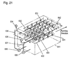
- Fig. 21 is a schematic view of a conventional etching apparatus as a manufacturing apparatus of printed wiring boards.
- plural upper surface nozzle pipes 632 and plural lower surface nozzle pipes 633 disposed in an etching booth 641 are respectively provided with a plurality of spray nozzles 631.
- An upper surface spray pump 638 supplies an etchant into an upper surface nozzle pipe 632 through an upper surface pressure regulating valve 636.
- a lower surface spray pump 639 supplies an etchant into a lower surface nozzle pipe 633 through a lower surface pressure regulating valve 637.
- the pressure of the etchant is checked respectively at an upper surface pressure gauge 634 and a lower surface pressure gauge 635.
- a feed roller 640 is used for convey a printed wiring board 642 in a running direction.
- a printed wiring board 642 forming an etching resist by screen printing method or photographic method on a copper lined laminate board (not shown) cut in specified size is conveyed into an etching booth 631 between plural upper surface nozzle pipes 632 and plural lower surface nozzle pipes 633 disposed parallel to or at a certain angle to the running direction of the printed wiring board 642, and conveyed on a roller 640 at a specified speed in the running direction, and sprayed with an etchant as a treating solution such as cupric chloride on both upper and lower surfaces by means of spray nozzles 631 to dissolve (etch) the exposed copper in the etching resist non-forming area, and a conductor pattern is obtained.
- an etchant as a treating solution such as cupric chloride
- the upper surface nozzle pipes 632 and lower surface nozzle pipes 633 can be oscillated at an angle of 45° to 60° to the running direction of the printed wiring board 642. Later, through the etching resist stripping, washing and drying steps, a conductor pattern is formed from the copper lined laminate board.
- a manufacturing apparatus of printed wiring board of the invention comprises a feed roller for conveying a printed wiring board at a specified speed, plural nozzle pipes mounting a plurality of spray nozzles and disposed nearly at uniform intervals parallel to or at a certain angle to the running direction of the printed wiring board, a mechanism for oscillating the nozzle pipes, and a pump for supplying a treating solution to the nozzle pipes, in which the plural nozzle pipes are composed of nozzle pipes having different apertures, or plural piping pipes are disposed between the plural nozzle pipes and the pump, and in particular the aperture of the nozzle pipe positioned in the center is larger than the aperture of the nozzle pipes at both sides, or the aperture of the piping pipe connected to the nozzle pipe in the center is larger than the aperture of the piping pipes at both sides.
- a manufacturing method of printed wiring board of the invention is to manufacture a printed wiring board by using such manufacturing apparatus of printed wiring board.
- the flow rate distribution of the treating solution sprayed from the spray nozzles to the printed wiring board can be set so as not to be stagnant on the printed wiring board, and etching of high precision is realized, and further the printed wiring board can be conveyed easily at specified speed, so that the manufacturing apparatus can be presented without lowering the productivity or hiking the apparatus manufacturing cost.
- a manufacturing apparatus of printed wiring board in other aspect of the invention comprises a feed roller for conveying a printed wiring board at a specified speed, plural nozzle pipes mounting a plurality of spray nozzles and disposed at specified intervals parallel to or at a certain angle to the running direction of the printed wiring board, a mechanism for oscillating the nozzle pipes, a pump for supplying an etchant as a treating solution to the nozzle pipes, and a pressure regulating valve and a pressure gauge connected in an individual passage between the pump and each nozzle pipe, in which nozzle pipes are disposed at narrower intervals at central positions among other plural nozzle pipes.
- the etching speed is uniform in the central area and peripheral area, and upper surface and lower surface of the printed wiring board, so that a conductor pattern of high precision can be formed.
- a manufacturing method of printed wiring board using this manufacturing apparatus of printed wiring board is characterized by setting so that the indication of the pressure gauge of the nozzle pipe in the center may be higher than the indication of the pressure gauges of the nozzle pipes at both sides by controlling the opening degree of the individual pressure regulating valves, oscillating the nozzle pipes at a constant angle, and etching by conveying at a specified speed while spraying the etchant to the printed wiring board.
- the pressure of the central nozzle pipe may be set higher than the pressure of the nozzle pipes at both sides easily by controlling the opening degree of the pressure regulating valves while observing the indication of the pressure gauges.
- the etching speed is made uniform in the central area and peripheral area and on the upper surface and lower surface, and a conductor pattern of high precision is formed, so that a simple etching apparatus of printed wiring board is presented without lowering the productivity or hiking the apparatus manufacturing cost.
- a manufacturing apparatus of printed wiring board in a different aspect of the invention comprises a feed roller for conveying a printed wiring board at a specified speed, plural nozzle pipes mounting a plurality of spray nozzles and disposed parallel to or at a certain angle to the running direction of the printed wiring board, a mechanism for oscillating the nozzle pipes, and a pump for supplying an etchant as a treating solution to the nozzle pipes, in which the mechanism for oscillating the nozzle pipes is disposed independently in each nozzle pipe.
- the conditions of the oscillating angle and oscillating speed of nozzle pipes can be set independently in individual nozzle pipes.
- the flow of the etchant on the printed wiring board may be set so that the etching force may be uniform.
- a manufacturing method of printed wiring board using this manufacturing apparatus of printed wiring board is characterized by setting the oscillating angle of the central nozzle pipe smaller than the oscillating angle of the nozzle pipes at both sides, setting the oscillating speed higher, and conveying at a specified speed while spraying the etchant to the printed wiring board, thereby etching the printed wiring board.
- the etchant in the central area of the upper surface does not stay still but immediately flows down, and therefore the etching speed is uniform in the central area and peripheral area and on the upper surface and lower surface, so that a conductor pattern of high precision may be formed.
- a manufacturing apparatus of printed wiring board in a further aspect of the invention comprises a feed roller for conveying a printed wiring board at a specified speed, plural nozzle pipes mounting a plurality of spray nozzles and disposed parallel to or at a certain angle to the running direction of the printed wiring board, a mechanism for oscillating the nozzle pipes, a pump for supplying an etchant as a treating solution to the nozzle pipes, and a pressure-proof flexible tube disposed between each one of the plural nozzle pipes and the pump.
- the pressure-proof flexible tube is disposed between each nozzle pipe and pump, the interval between nozzle pipes and moving of position in the vertical direction are free, and the etching apparatus easy in condition setting of printed wiring board where high precision is required can be presented.
- a manufacturing method of printed wiring board using this apparatus is characterized by etching a printed wiring board by oscillating the nozzle pipes at specified oscillating angle and oscillating speed, and conveying at specified speed while blowing etchant to the printed wiring board, by using the manufacturing apparatus of printed wiring board capable of varying the interval of individual nozzle pipes, or varying in the vertical direction.
- the amount of etchant sprayed to the central area on the printed wiring board is increased, and by bringing the position of the central nozzle pipes closer to the board conveying surface side, the impingement of the etchant on the central area of the printed wiring board is set stronger than that of the peripheral area, so that the etchant flows down efficiently and promptly without staying in the upper surface central area of the printed wiring board, and the etching speed is uniform in the central area and peripheral area and on the upper surface and lower surface, so that a conductor pattern of higher precision is formed.
- a manufacturing apparatus of printed wiring board in a further different aspect of the invention comprises a feed roller for conveying a printed wiring board at a specified speed, plural nozzle pipes mounting a plurality of spray nozzles and disposed parallel to or at a certain angle to the running direction of the printed wiring board, a mechanism for oscillating the nozzle pipes, plural pumps for supplying an etchant as a treating solution to the nozzle pipes, the plural pumps corresponding to the nozzle pipes, and a pressure gauge connected in an individual passage between each nozzle pipe and the pump, in which the output of each pump is controlled by an inverter circuit or a current or voltage control circuit.
- the etching apparatus capable of setting the conditions of the printed wiring board where high precision is required easily and automatically can be presented.
- a manufacturing method of printed wiring board using this apparatus is characterized by etching a printed wiring board by conveying at specified speed while blowing etchant as treating solution to the printed wiring board by oscillating the nozzle pipes at a constant angle, by controlling the output of each pump so that the indication of the pressure gauge of the central nozzle pipe may be higher than the indication of the pressure gauges of the nozzle pipes at both sides.
- the pressure of the central nozzle pipe may be easily set so as to be higher than the pressure of the nozzle pipes at both sides, and the etchant flows down efficiently and promptly without staying in the central area of the upper surface of the printed wiring board, and the etching speed is uniform in the central area and peripheral area and on the upper surface and lower surface, so that a conductor pattern of higher precision is formed.
- the manufacturing apparatus of printed wiring board having such configuration may be modified as follows in order to automate setting of the etching condition. That is, in the case of having N nozzle pipes for processing a printed wiring board, it comprises means for dividing at least into N regions by dividing line parallel in the running direction of the printed wiring board beforehand and storing data of processing area of each divided block, means for storing correction data of each nozzle pipe, means for selecting correction data corresponding to each divided block as output data, means for calculating the final output data to each spray pump from the selected output data, and means for controlling the spray pump output corresponding to the final output data.
- the printed wiring board is divided into N regions parallel in the running direction, and depending on the processing area of each region, that is, the etching area, and the etching force by the piping position of nozzle pipes, by controlling the pressure setting of each nozzle pipe by the pump output, the etching condition can be set automatically.
- FIG. 1 shows an outline of a manufacturing apparatus of printed wiring board in embodiment 1 of the invention
- Fig. 2 is a schematic diagram showing the detail of the manufacturing apparatus in embodiment 1 of the invention.
- plural upper surface nozzle pipes 102a to 102f disposed nearly at equal intervals in an etching booth 111 are individually provided with a plurality of spray nozzles 101, and are disposed parallel to or at a certain angle to the running direction of the printed wiring board.
- plural lower surface nozzle pipes 103a to 103f disposed nearly at equal intervals in the etching booth 111 are individually provided with a plurality of spray nozzles 101, and are disposed parallel to or at a certain angle to the running direction of the printed wiring board.
- An upper surface spray pump 108 supplies an etchant to the nozzle pipes 102a to 102f.
- a lower surface spray pump 109 supplies an etchant to the nozzle pipes 103a to 103f.
- a feed roller 110 conveys a printed wiring board 112 at a specified speed.
- the aperture of the central nozzle pipes 102c, 102d, 103c, 103d is about 20 to 30% larger than that of the nozzles pipes at both sides 102a, 102b, 102e, 102f.
- piping pipes 104a to 104f are disposed between the upper surface spray pump 108 and upper surface nozzle pipes 102a to 102f.
- Piping pipes 105a to 105f are disposed between the lower surface spray pump 109 and lower surface nozzle pipes 103a to 103f.
- the aperture of the piping pipes 104c, 104d, and 105c, 105d connected to the central nozzle pipes 102c, 102d, and 103c, 103d is about 20 to 30% larger than that of the piping pipes at both sides 104a, 104b and 105e, 105f.
- a printed wiring board 112 is prepared by forming an etching resist by screen printing method or photographic method on a copper lined laminate board (not shown) cut in a specified size and having a copper foil of 35 ⁇ m in thickness formed on both sides of an insulating substrate.
- This printed wiring board 112 is conveyed into the etching booth 111 between the upper surface nozzle pipes 102a to 102f and lower surface nozzle pipes 103a to 103f disposed parallel to or at a certain angle to the running direction, at a specified speed on the feed roller 110, and is etched by blowing an etchant such as cupric chloride on both upper and lower surfaces from spray nozzles 101.
- an etchant such as cupric chloride
- the upper surface nozzle pipes 102a to 102f and lower surface nozzle pipes 103a to 103f are oscillated at an angle of 45° to 60° within a plane at right angle to the running direction of the printed wiring board in the blowing direction of the spray nozzles on the axis of rotation of the axis of each nozzle pipe.
- a joint for rotating only the nozzle pipes is needed so as not to leak the etchant at the junction from the spray pump to each nozzle pipe, but it is not shown in the diagram.
- the aperture of the central nozzle pipes 102c, 102d, 103c, 103d is increased by about 20 to 30% as compared with that of the nozzle pipes at both sides 102a, 102b and 103e, 103f, and hence the etchant in the central area of the upper surface of the printed wiring board does not stay still but immediately flows down from both sides, so that the entire surface of the printed wiring board may be always etched with a fresh etchant.
- nozzle pipes and piping pipes in the central area are set larger in aperture, but the nozzle pipes 102b, 102e, 103b, 103e, and piping pipes 104b, 104e, 105b, 105e being adjacent to the central nozzle pipes and piping pipes may be also set larger in aperture by 10 to 20% as compared with that of the remotest side nozzle pipes and piping pipes, and the same effects are obtained.
- the etching apparatus for etching of copper foil is explained, but the invention may be similarly applied also in the developing apparatus for developing and removing unexposed portion of photosensitive resist.
- FIG. 3 is an outline diagram of a manufacturing apparatus of printed wiring board in embodiment 2 of the invention
- Fig. 4 is a detailed diagram of the manufacturing apparatus of printed wiring board in embodiment 2 of the invention.
- plural upper surface nozzle pipes 202a to 202e disposed in an etching booth 211 are individually provided with a plurality of spray nozzles 201, and are disposed parallel to or at a certain angle to the running direction of the printed wiring board.
- plural lower surface nozzle pipes 203a to 203e are individually provided with a plurality of spray nozzles 201, and are disposed parallel to or at a certain angle to the running direction of the printed wiring board.
- An upper surface spray pump 208 supplies an etchant to the nozzle pipes 202a to 202e through upper surface pressure regulating valves 206a to 206e as means for regulating the spray pressure.
- Upper surface pressure gauges 204a to 204e monitor the pressure of the nozzle pipes 202a to 202e after passing through the upper surface pressure regulating valves 206a to 206e.
- a lower surface spray pump 209 supplies an etchant to the nozzle pipes 203a to 203e through lower surface pressure regulating valves 207a to 207e as means for regulating the spray pressure.
- Lower surface pressure gauges 205a to 205e monitor the pressure of the nozzle pipes 203a to 203e after passing through the lower surface pressure regulating valves 207a to 207e.
- a feed roller 210 conveys a printed wiring board 212 in the running direction.
- the etching apparatus as the manufacturing apparatus of printed wiring board having such configuration is as shown in Fig. 4, in which the interval of the central nozzle pipes 202c and 202b, and 202c and 202d is about 10 to 30% narrower than the interval of other nozzle pipes 202a and 202b, and 202d and 202e, and in this structure, therefore, the amount of etchant blown to the central part on the printed wiring board can be increased.
- the number of nozzle pipes is five, 202a to 202e, but in the case of six pipes 202a to 202f (not shown), the interval of the central pipes 202c and 202d is about 30 to 50% narrower than the interval of other nozzle pipes 202a and 202b, and 202e and 202f, and as required, the interval of the nozzle pipes closer to the center 202b and 202c, and 202d and 202e may be set about 10 to 30% narrower.
- a printed wiring board 212 is prepared by forming an etching resist by screen printing method or photographic method on a copper lined laminate board (not shown) cut in a specified size and having a copper foil of 35 ⁇ m in thickness formed on both sides of an insulating substrate.
- This printed wiring board 212 is conveyed into the etching booth 211 between the upper surface nozzle pipes 202a to 202e and lower surface nozzle pipes 203a to 203e disposed parallel to or at a certain angle to the running direction, at a specified speed on the feed roller 210, and is etched by blowing an etchant such as cupric chloride on both upper and lower surfaces from spray nozzles 201.
- an etchant such as cupric chloride
- the upper surface nozzle pipes 202a to 202e and lower surface nozzle pipes 203a to 203e are oscillated at an angle of 45° to 60° within a plane at right angle to the running direction of the printed wiring board, and the etchant supplied from the upper surface spray pump 208 to the upper surface nozzle pipes 202a to 202e is regulated by the opening degree of the upper surface pressure regulating valves 206a to 206e, and the spray pressure indicated on upper surface pressure gauges 204a to 204e is adjusted.
- the etchant supplied from the lower surface spray pump 209 to the lower surface nozzle pipes 203a to 203e is regulated by the opening degree of the lower surface pressure regulating valves 207a to 207e, and the spray pressure indicated on lower surface pressure gauges 205a to 205e is adjusted.
- the pressure indicated on upper surface pressure gauges 204a to 204e is adjusted by the opening degree of the upper surface pressure regulating valves 206a to 206e so that the pressure may be high in the central nozzle pipe, that is, 1.2 kg/cm 2 in the gauge 204a, 1.6 kg/cm 2 in the gauge 204b, 2.0 kg/cm 2 in the gauge 204c, 1.6 kg/cm 2 in the gauge 204d, and 1.2 kg/cm 2 in the gauge 204e.
- the pressure indicated on lower surface pressure gauges 205a to 205e is adjusted by the opening degree of the lower surface pressure regulating valves 207a to 207e, that is, 1.0 kg/cm 2 in the gauge 205a, 0.9 kg/cm 2 in the gauge 205b, 0.8 kg/cm 2 in the gauge 205c, 0.9 kg/cm 2 in the gauge 205d, and 1.0 kg/cm 2 in the gauge 205e.
- the pressure setting value of the central nozzle pipe 204c is somewhat higher but the pressure balance is relatively moderate because the piping interval of the central nozzle pipes is narrow and the amount of etchant injected to the central area on the printed wiring board is relatively larger than in the peripheral area so that the setting may be somewhat lower as compared with the case of equal piping interval of nozzle pipes.
- Injection pressure to plural nozzles attached to each nozzle pipe is not extremely low, and probability of trouble due to clogging of foreign matter in the etchant injection port of the nozzle can be lowered. Moreover, since the pressure at both sides is low, the fluid loss due to closing of pressure regulating valve and narrowing of etchant passage can be lowered, and the energy efficiency is enhanced.
- the flow rate regulating valve generally has graduations for adjustment of flow rate, and it is same as the pressure regulating valve in its principle. In the explanation of the embodiment of the invention, the pressure regulating valve and flow rate regulating valve are handled differently.
- the etching flow rate per unit time blown on the printed wiring board may differ. That is, when the etchant injection port of the nozzle is small, if the pressure gauge indicates the same, the flow rate of the etchant injected onto the printed wiring board is smaller as compared with the case of a large injection port. Accordingly, when the nozzle is clogged with foreign matter, the pressure of the pressure gauge elevates, but the flow rate of the etchant decreases. It is actually difficult to detect nozzle clogging during production.
- the pressure regulating valve When managed by the pressure only, in order to lower the indication of the pressure gauge, the pressure regulating valve is controlled in the closing direction, but the flow rate blown onto the printed wiring board is further decreased at this time, and such contradictory conditions may be set.
- the etching apparatus generally comprises, in order to remove foreign matter, a filter installed between the spray pump and nozzle pipe, or between the etchant reservoir in the bottom of the etching apparatus main body and the spray pump.
- a filter installed between the spray pump and nozzle pipe, or between the etchant reservoir in the bottom of the etching apparatus main body and the spray pump.
- the pressure gauge may indicate the same value as the initial correct setting.
- the flow rate of the etchant blown onto the printed wiring board is extremely decreased due to decrease of flow rate due to clogging of spray nozzle and decrease of flow rate due to clogging of filter, and in an extreme case, the flow rate of the etchant may not reach the level for etching the thickness of the copper sufficiently, and the copper layer be left over.
- the flow rate of the etchant per unit time blown onto the printed wiring board may be kept constant, and the printed wiring board may be manufactured in stable conditions.
- the printed wiring board is a two-sided printed wiring board without through hole plating, but it may be also applied in a one-sided printed wiring board, a two-sided printed wiring board with through hole plating, or a multilayer printed wiring board
- the etching resist is an organic material formed by screen printing method or photographic method, but solder or other metal resist or photosensitive electrodeposition resist may be used.
- the etchant is cupric chloride, but ferric chloride, ammonia or other alkaline etchant may be also used.
- the copper lined laminate board is prepared by cutting to a specified size and forming 35 ⁇ m thick copper foils on both sides of an insulating substrate, but it is evident from the configuration of the invention that it is easily applied in various board sizes or different etching precisions or conductor thicknesses by adjusting the set pressure.
- the etching apparatus for etching of copper foil is explained, but the invention may be similarly applied also in the developing apparatus for developing and removing unexposed portion of photosensitive resist.
- FIG. 5 and Fig. 6 are outline diagrams of an etching apparatus as a manufacturing apparatus of printed wiring board in embodiment 3 of the invention
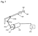
- Fig. 7 is a detailed diagram of an oscillating mechanism of nozzle pipes of the manufacturing apparatus in the embodiment of the invention.
- etching apparatus in embodiment 3 of the invention is similar to a conventional apparatus for etching from both upper surface and lower surface simultaneously, and the upper structure and lower structure are basically the same. For the ease of explanation of the invention, therefore, only the upper structure is explained by referring to the drawings.
- upper surface nozzle pipes 302a to 302f are disposed parallel to or at an angle of 1 to 5° to the running direction of a printed wiring board 308 to be conveyed by a feed roller 306 into a first etching booth 307a as a first treating booth.
- the upper surface nozzle pipes are provided with upper surface pressure regulating valves 304a to 304f as means for regulating the spray pressure from an upper surface spray pump 305 for supplying an etchant as treating solution.
- the nozzle pipes are also provided with upper surface pressure gauges 303a to 303f, and the nozzle pipes are further equipped with independent oscillating mechanisms 309a to 309f for individual upper surface nozzle pipes.
- Fig. 6 shows two etching booths, that is, a second etching booth 307b as a second treating booth aside from the first etching booth 307a, and in the first etching booth 307a, upper surface nozzle pipes 302a to 302f are disposed at an angle of 1 to 5° to the running direction of the printed wiring board 308, and in the second etching booth 307b, upper surface nozzle pipes 302a' to 302f' are disposed at an angle of 1 to 5° in the reverse direction of the nozzle pipes in the first etching booth.
- Fig. 7 shows the detail of an independent oscillating mechanism of a pipe in the embodiment 3 of the invention.
- An independent oscillating mechanism for each nozzle pipe comprises a cam (rotating disk) 311 and link mechanisms 312a, 312b, and the oscillating angle can be varied by moving positions of the fulcrum 312c of the link mechanism on the rotating disk.
- the cam 311 is directly coupled to a control motor 310, or is interlocked by belt or gear, and the control motor 310 is easily changed in the rotating speed by means of an inverter circuit 313.
- the oscillating angle and oscillating speed can be varied independently.
- condition setting is explained in the etching apparatus using only the first etching booth 307a of printed wiring board in Fig. 5 relating to embodiment 3 of the invention.
- the oscillating angle of the central nozzle pipes 303c and 303d is set smaller than the oscillating angle of the other nozzle pipes 303a and 303b, and 303e and 303f, by moving the position of the fulcrum 312c of the link mechanism in the oscillating mechanism shown in Fig. 7. Further, the oscillating speed of the central nozzle pipes 303c and 303d is set larger than that of the other nozzle pipes 303a and 303b, and 303e and 303f, by means of the inverter circuit 313 or current or voltage control circuit.
- the etchant does not stay in the central area of the upper surface, but immediately flows down.
- a printed wiring board 308 is prepared by forming an etching resist by screen printing method or photographic method on a copper lined laminate board (not shown) cut in a specified size and having a copper foil of 35 ⁇ m in thickness formed on both sides of an insulating substrate.
- This printed wiring board 308 is conveyed into the etching booths 307a, 307b between the upper surface nozzle pipes 302a to 302f and lower surface nozzle pipes not shown disposed parallel to or at a certain angle to the running direction, at a specified speed on the feed roller 306, and is etched by blowing an etchant such as cupric chloride on both upper and lower surfaces from spray nozzles 301.
- an etchant such as cupric chloride
- the upper surface nozzle pipes 302a to 302f and lower surface nozzle pipes are oscillated at independent oscillating angles and oscillating speeds individually, to the running direction of the printed wiring board, by setting the oscillating angle at 45° for the central nozzle pipes 302c and 302d, and 60° for the other nozzle pipes 302a and 302b, and 302e and 302f, and the etchant supplied from the upper surface spray pump 305 to the upper surface nozzle pipes 302a to 302f is regulated by the opening degree of the upper surface pressure regulating valves 304a to 304f, and the spray pressure indicated on upper surface pressure gauges 303a to 303f is adjusted.
- the etchant supplied from the lower surface spray pump not shown to the lower surface nozzle pipes is regulated by the opening degree of the lower surface pressure regulating valves not shown, and the spray pressure indicated on lower surface pressure gauges is adjusted.
- the pressure indicated on upper surface pressure gauges 303a to 303f is adjusted by the opening degree of the upper surface pressure regulating valves 304a to 304f so that the pressure may be high in the central nozzle pipe, that is, 1.2 kg/cm 2 in 303a, 1.6 kg/cm 2 in 303b, 2.0 kg/cm 2 in 303c, 2.0 kg/cm 2 in 303d, 1.6 kg/cm 2 in 303e, and 1.2 kg/cm 2 in 303f.
- the pressure indicated on lower surface pressure gauges is adjusted to appropriate values by the opening degree of the lower surface pressure regulating valves depending on the number of feed rollers and configuration.
- etching apparatus of printed wiring board having at least two etching booths, that is, first etching booth 307a and second etching booth 307b.
- the oscillating angle of the central nozzle pipes 302c and 302d is set smaller than the oscillating angle of both side nozzle pipes 302a and 302 ⁇ , and 302e and 302f, by moving the positions of the fulcrum on the rotating disk of the oscillating mechanism of link mechanism, and the rotating speed of the control motor is increased by using the inverter circuit or current or voltage control circuit, and the oscillating speed is increased.
- the oscillating angle of the central nozzle pipes is set smaller than the oscillating angle of the both side nozzle pipes, and the oscillating speed is set larger, and also the oscillating angle is set larger than that of the corresponding nozzle pipes of the first etching booth, and the oscillating speed is set smaller.
- other oscillating mechanism is needed for plural nozzle pipes of the second etching booth, but its illustration is omitted.
- the side etching amount (etching amount in the lateral direction) is decreased, and the oscillating speed is increased, so that stagnant etchant in the central area may be avoided.
- the etching apparatus may comprise pressure gauges and pressure regulating valves for nozzle pipes, and in addition to setting of oscillating angle and oscillating speed of nozzle pipes in the first etching booth and second etching booth, by adjusting the pressure of each nozzle pipe, etching conditions of higher precision can be set.
- the printed wiring board 308 is a two-sided printed wiring board without through hole plating, but it may be also applied in a one-sided printed wiring board, a two-sided printed wiring board with through hole plating, or a multilayer printed wiring board, and the etching resist is an organic material formed by screen printing method or photographic method, but solder or other metal resist or photosensitive electrodeposition resist may be used.
- the etchant is cupric chloride, but ferric chloride, ammonia or other alkaline etchant may be also used.
- the copper lined laminate board is prepared by cutting to a specified size and forming 35 ⁇ m thick copper foils on both sides of an insulating substrate, but it is evident from the configuration of the invention that it is easily applied in various board sizes or different etching precisions or conductor thicknesses by adjusting the set pressure.
- the etching apparatus for etching of copper foil is explained, but the invention may be similarly applied also in the developing apparatus for developing and removing unexposed portion of photosensitive resist.
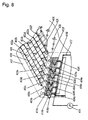
- FIG. 8 is an outline diagram of an etching apparatus as a manufacturing apparatus of printed wiring board in embodiment 4 of the invention
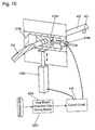
- Fig. 9 and Fig. 10 are detailed diagrams of an independent nozzle pipe of the manufacturing apparatus of printed wiring board in embodiment 4 of the invention
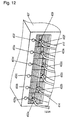
- Fig. 11 and Fig. 12 are diagrams showing the condition setting of the manufacturing apparatus of printed wiring board in embodiment 4 of the invention.
- An etching apparatus is explained as the manufacturing apparatus of printed wiring board in this embodiment.
- the configuration of the etching apparatus of the embodiment is similar to a conventional apparatus for etching from both upper surface and lower surface simultaneously, and the upper structure and lower structure are basically the same. For the ease of explanation of the invention, therefore, only the upper structure is explained by referring to the drawings.
- upper surface nozzle pipes 402a to 402f are disposed parallel to or at an angle of 1 to 5° to the running direction of a printed wiring board 408 in an etching booth 407.
- the plural upper surface nozzle pipes 402a to 402f are provided with a plurality of spray nozzles 401.
- Each upper surface nozzle pipe is connected to an upper surface spray pump 405 for supplying an etchant as treating solution through pressure-proof flexible tubes 414a to 414f.
- upper surface pressure regulating valves 404a to 404f as means for regulating the spray pressure are provided together with the upper surface pressure gauges 403a to 403f provided at the downstream side.
- the printed wiring board 408 is conveyed at a specified speed in the running direction indicated by arrow by a feed roller 406.
- a nozzle pipe, for example, 402a penetrates through a first support member 415a, and is supported by an oscillating mechanism 409a so as to be oscillated.
- the first support member 415a is supported by a second support member 415b so as to be movable in the lateral direction in the second support member 415b.
- the second support member 415b is supported to be movable vertically in the moving region of front wall and rear wall (not shown) of the etching booth 407.
- a first bellows member 416a is disposed in the moving region in the lateral direction of the first support member 415a
- a second bellows member 416b is disposed in the moving region in the vertical direction of the second support member 415b.
- linear motion is employed as the means for moving the first support member 415a and second support member 415b.
- first support member 415a is moved by a motor driven cylinder 418a as linear motion
- second support member 415b is moved by a motor driven cylinder 418b also as linear motion.
- the mounting position of the motor driven cylinder 418a must be considered so as not to contact with adjacent nozzle pipes.
- the motor driven cylinders 418a, 418b control the moving position by a control circuit 419, and the control circuit 419 is operated by a signal from input means 420a. In this configuration, each nozzle pipe can be moved automatically.
- the input means 420a may be replaced by dimensional data storing means 420b as means for entering and converting dimensional data of printed wiring board, and dimensional data may be entered therein.
- the interval of nozzle pipes may be set automatically.
- the dimension of the printed wiring board in the lateral direction to the running direction is measured preliminarily, and is fed into the dimensional data storing means 420b, and after moving and setting the intervals of the nozzle pipes corresponding to the dimensional data, etching is performed. That is, as compared with the case of etching the printed wiring board having the lateral direction dimension of 600 mm, in the case of etching of the printed wiring board having a dimension of 400 mm, the interval of nozzle pipes is set narrower.
- the printed wiring board can be manufactured in the condition of the highest etching efficiency depending on the dimension of the printed wiring board.
- the upper surface nozzle pipes 402a to 402f are equipped with independent oscillating mechanisms.
- Independent oscillating mechanism 409a to 409f shown in Fig. 11 corresponding to the upper surface nozzle pipes 402a to 402f are individually composed of a cam 411 and a link mechanism 412a as shown in Fig. 9, and the oscillating angle can be varied by moving the positions of the fulcrum 412b on the rotating disk of the link mechanism.
- the cam (rotating disk) 411 is directly coupled to a control motor 410, or is interlocked by belt or gear, and the control motor 410 is easily changed in the rotating speed by means of an inverter circuit 413.
- the independent nozzle pipes are supported by the first support member 415a as shown in Fig. 9, and partly fixed on the same first support member 415a in an oscillatable state, and coupled with a flexible wire 417 interlocked with the fulctrum 412b of the rotating disk of the link mechanism, so as to oscillate by the forward and backward motion of the wire.
- the moving distance of the flexible wire 417 is varied by moving the position of the fulcrum 412b of the link mechanism, so that the oscillating angle can be changed.
- the wire moving speed is changed by the number of revolutions of the cam (rotating disk) 411. In this structure, if the nozzle pipes move laterally and vertically, it is possible to keep independence of the oscillating angle and oscillating speed in the oscillating mechanism of each nozzle pipe.
- the etching precision usually fluctuates largely on the upper surface as explained in the mechanism of the prior art.
- the etchant is not collected in the central area of the printed wiring board as seen on the upper surface, but only a slight fluctuation may be caused due to blocking of contact of the injected etchant with the printed wiring board owing to the presence of the roller for conveying the printed wiring board.
- condition setting on the upper surface of the printed wiring board of the etching apparatus is explained in the following two cases: (1) setting of mutual interval of nozzle pipes, oscillating angle, oscillating speed, and pressure of etchant, and (2) setting of distance of nozzle pipe from board conveying surface, oscillating angle, oscillating speed, and pressure of etchant.
- the distance of the central nozzle pipes 402c and 402d from the board conveying surface is about 30 to 50% shorter than the distance of other nozzle pipes 402a and 402b, and 402e and 402f from the board conveying surface, and as required, the distance of the nozzle pipes closer to the center 402b and 402e from the board conveying surface may be set about 10 to 30% shorter.
- the spray pressure of each nozzle pipe is set as follows as the third setting.
- the pressure indicated on upper surface pressure gauges 403a to 403f is adjusted by the opening degree of the upper surface pressure regulating valves 404a to 404f so that the pressure may be high in the central nozzle pipes, that is, 1.2 kg/cm 2 in 403a, 1.6 kg/cm 2 in 403b, 2.0 kg/cm 2 in 403c, 2.0 kg/cm 2 in 403d, 1.6 kg/cm 2 in 403e, and 1.2 kg/cm 2 in 403f.
- the pressure of the two central nozzle pipes is set higher than the pressure of the other nozzle pipes, but what differs from case (1) is that since the distance from the printed wiring board is shorter, the pressure in the central area can be set lower as comparative value, and further the pressure of other nozzle pipes may be set higher, and the etching speed can be increased on the whole, so that the productivity may be higher than in case (1).
- each nozzle pipe may be wider by bringing the central nozzle pipes further closer to the board conveying surface, bringing the central both side nozzle pipes closer than nozzle pipes at outer most ends, or adjusting the oscillating angle and oscillating speed of the nozzle pipes.
- This printed wiring board 408 is conveyed into the etching booths 407 between the upper surface nozzle pipes 402a to 402f and lower surface nozzle pipes disposed parallel to or at a certain angle to the running direction, at a specified speed on the feed roller 406, and is etched by blowing an etchant such as cupric chloride on both upper and lower surfaces from spray nozzles 401.
- an etchant such as cupric chloride
- the upper surface nozzle pipes 402a to 402f and lower surface nozzle pipes are oscillated at independent oscillating angles and oscillating speeds individually, within a plane at right angle to the running direction of the printed wiring board, by setting the oscillating angle at 45° for the central nozzle pipes 402c and 402d, and 60° for the other nozzle pipes 402a and 402b, and 402e and 402f, and the etchant supplied from the upper surface spray pump 405 to the upper surface nozzle pipes 402a to 402f is regulated by the opening degree of the upper surface pressure regulating valves 404a to 404f, and the spray pressure indicated on upper surface pressure gauges 403a to 403f is adjusted.
- the pressure setting of the nozzle pipes can be adjusted finely, and the condition can be set easily by the pressure regulating valve while observing the indication of pressure gauge of each nozzle pipe.
- condition setting is mainly explained about the upper surface of the printed wiring board.
- Condition setting of the lower surface of the printed wiring board generally differs in each etching apparatus, depending on the number of feed rollers, roller pitch, and mounting position.
- the etching conditions of the lower surface of the printed wiring board in each etching apparatus are set by adjusting the mutual interval of nozzle pipes, distance from the board conveying surface, and oscillating angle and oscillating speed of the nozzle pipes. After setting roughly uniform etching conditions on the entire surface of the printed wiring board, same as in the case of the upper surface of the printed wiring board, fine adjustment is achieved by regulating the pressure of each nozzle pipe again.
- the condition setting of the etching apparatus is explained in two cases: (1) setting of mutual interval of nozzle pipes, oscillating angle, oscillating speed, and pressure of etchant, and (2) setting of distance of nozzle pipe from board conveying surface, oscillating angle, oscillating speed, and pressure of etchant.
- the etching conditions may be set in other combinations, for example, (3) setting of interval of nozzle pipes, distance from board conveying surface, and pressure, and (4) setting of interval of nozzle pipes, distance from board conveying surface, oscillating angle and oscillating speed.
- the conditions may be set by including all cases, that is, (5) setting of interval of nozzle pipes, distance from board conveying surface, oscillating angle, oscillating speed, and pressure.
- the etching apparatus for etching of copper foil is explained, but the invention may be similarly applied also in the developing apparatus for developing and removing unexposed portion of photosensitive resist.
- Embodiment 5 of the invention is described by referring to the accompanying drawings.
- Fig. 13 and Fig. 14 are outline diagrams of an etching apparatus as a manufacturing apparatus of printed wiring board in embodiment 5 of the invention
- Fig. 15 (a) and Fig. 15 (b) are detailed diagrams of an oscillating mechanism of nozzle pipes of the etching apparatus as the manufacturing apparatus in embodiment 5 of the invention.
- the configuration of the etching apparatus in the embodiment of the invention is similar to a conventional apparatus for etching from both upper surface and lower surface simultaneously, and the upper structure and lower structure are basically the same. For the ease of explanation of the invention, therefore, only the upper structure is explained by referring to the drawings.
- upper surface nozzle pipes 502a to 502f are disposed parallel to or at an angle of 1 to 5° to the running direction of a printed wiring board to be conveyed by a feed roller 506 into a first etching booth 507a.
- the nozzle pipes have a plurality of spray nozzles each, and are provided with independent oscillating mechanisms 509a to 509f.
- Plural upper surface spray pumps 504a to 504f controlled by corresponding inverter circuits 505a to 505f supply an etchant as treating solution to the corresponding nozzle pipes 502a to 502f.
- the nozzle pipes are provided with corresponding upper surface pressure gauges 503a to 503f.
- Fig. 14 shows two etching booths, that is, a first etching booth 507a as a first treating booth, and a second etching booth 507b as a second treating booth, in which upper surface nozzle pipes 502a to 502f are disposed at a angle of 1 to 5° to the running direction of the printed wiring board 508 in the first etching booth 507a, and upper surface nozzle pipes 502a' to 502f' are disposed at an angle (reverse angle) of 1 to 5° in the reverse direction of the nozzle pipes in the first etching booth in the second etching booth 507b.
- Fig. 15 (a) shows the detail of an independent oscillating mechanism of a nozzle pipe in the embodiment.
- An independent oscillating mechanism corresponding to each nozzle pipe comprises a cam (rotating disk) 511 and link mechanisms 512a, 512b, and the oscillating angle can be varied by moving the position of the fulcrum 512c of the link mechanism on the rotating disk 511.
- the cam 511 is directly coupled to a control motor 510a, or is interlocked by belt or gear, and the control motor 510a is easily changed in the rotating speed by means of an inverter circuit 513a.
- the oscillating angle and oscillating speed can be varied independently.
- Fig. 15 (b) shows other example of an independent oscillating mechanism of a nozzle pipe.
- An independent oscillating mechanism corresponding to each nozzle pipe is coupled to a stepping motor 510b directly or by means of a gear, and the stepping motor 510b can easily change the oscillating angle and oscillating speed electrically by means of a control and drive circuit 513b.
- the oscillating angle of the central nozzle pipes 502c and 502d is set smaller than the oscillating angle of the other nozzle pipes 502a and 502b and 502e and 502f, by moving the position of the link fulcrum 512c on the cam 511 of the link mechanism in the oscillating mechanism, and further the oscillating speed of the central nozzle pipes 502c and 502d is set larger than that of the other nozzle pipes 502a and 502b and 502e and 502f, by means of the inverter circuit 513a or current or voltage control circuit.
- the etchant does not stay in the central area of the upper surface, but immediately flows down.
- a printed wiring board 508 is prepared by forming an etching resist by screen printing method or photographic method on a copper lined laminate board (not shown) cut in a specified size and having a copper foil of 35 ⁇ m in thickness formed on both sides of an insulating substrate.
- This printed wiring board 508 is conveyed into the etching booths 507a, 507b between the upper surface nozzle pipes 502a to 502f and lower surface nozzle pipes disposed parallel to or at a certain angle to the running direction indicated by arrow, at a specified speed on the feed roller 506, and is etched by blowing an etchant such as cupric chloride on both upper and lower surfaces from spray nozzles 501.
- an etchant such as cupric chloride
- the upper surface nozzle pipes 502a to 502f and lower surface nozzle pipes are oscillated at independent oscillating angles and oscillating speeds individually, within a plane at right angle to the running direction of the printed wiring board, by setting the oscillating angle at 45° for the central nozzle pipes 502c and 502d, and 60° for the other nozzle pipes 502a, 502b, and pipes 502e, 502f, and the etchant supplied from the upper surface spray pumps 504a to 504f to the upper surface nozzle pipes 502a to 502f is regulated by inverter circuits 505a to 505f of the upper surface spray pumps so that the output of the upper surface spray pumps 504a to 504f may indicate the specified spray pressure on the upper surface pressure gauges 503a to 503f.
- the etchant supplied from the lower surface spray pumps to the lower surface nozzle pipes is regulated by inverter circuits of the lower surface spray pumps so that the output of the lower surface spray pumps may indicate the specified spray pressure on the lower surface pressure gauges.
- the pressure indicated on upper surface pressure gauges 503a to 503f is adjusted by the inverter circuits 505a to 505f so that the pressure may be high in the central nozzle pipe, that is, 1.2 kg/cm 2 in the gauge 503a, 1.6 kg/cm 2 in the gauge 503b, 2.0 kg/cm 2 in the gauge 503c, 2.0 kg/cm 2 in the gauge 503d, 1.6 kg/cm 2 in the gauge 503e, and 1.2 kg/cm 2 in the gauge 503f.
- the pressure indicated on lower surface pressure gauges is adjusted to appropriate values by the inverter circuits depending on the number of feed rollers 506 and configuration.
- etching apparatus of printed wiring board having at least two etching booths, that is, first etching booth 507a and second etching booth 507b.
- the oscillating angle of the central nozzle pipes 502c and 502d of the first etching booth 507a is set smaller than the oscillating angle of both side nozzle pipes 502a, 502b, and pipes 502e, 502f, by moving the positions of the fluctrum position on the rotating disk of the rink mechanism of the oscillating mechanism , and the rotating speed of the control motor 510a is increased by using the inverter circuit 513a, and the oscillating speed is increased.
- the oscillating angle of the central nozzle pipes 502c' and 502d' is set smaller than the oscillating angle of the both side nozzle pipes, and the oscillating speed is set larger, and also the oscillating angle is set larger than that of the corresponding nozzle pipes of the first etching booth 507a, and the oscillating speed is set smaller.
- the first etching booth 507a by etching the central area of the printed wiring board at an angle close to vertical direction by heightening the injection pressure of the etchant, thereby decreasing the side etching amount and accelerating the oscillating speed, stagnant etchant in the central area is eliminated, and occurrence of side foot in the etching circuit is prevented in a wide range in the second etching booth 507b, and stagnant etchant in the central area is avoided, so that a printed wiring board of a higher precision may be manufactured.
- the side etching amount (etching amount in the lateral direction) is decreased, and stagnant etchant in the central area of printed wiring board may be avoided, and occurrence of side foot (lateral spread of conductor circuit) in the conductor circuit being etched in the second etching booth 507b is prevented, and over-etching is prevented, and stagnant etchant in the central area of printed wiring board is eliminated, so that a printed wiring board of a higher precision may be manufactured.
- the etching apparatus may comprise spray pumps and pressure gauges for nozzle pipes, and in addition to setting of oscillating angle and oscillating speed of nozzle pipes in the first etching booth and second etching booth, by adjusting the pressure of each nozzle pipe, etching conditions of higher precision can be set.
- the oscillating angle and oscillating speed are set by using the oscillating mechanism shown in Fig. 15 (a), but it is also possible to set the oscillating angle and oscillating speed automatically by using the oscillating mechanism shown in Fig. 15 (b) electrically, and in this case, too, the etching condition of the printed wiring board can be set similarly at high precision.
- Embodiment 6 of the invention is an example for automating setting of etching condition of printed wiring board.
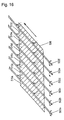
- Fig. 16 is a diagram showing a printed wiring board divided in N regions in embodiment 6 of the invention
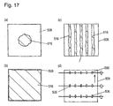
- Fig. 17 is a diagram showing the etching state of printed wiring board when setting the etching condition in embodiment 6 of the invention
- Fig. 18 and Fig. 19 are diagrams showing a drawing pattern of etching resist.
- the printed wiring board 508 is divided at least into six etching regions in the same number as the nozzle pipes, and they are supposed to be division blocks 515a to 515f.
- the etching apparatus of printed wiring board using photosensitive etching resist is coupled with the developing apparatus in the preceding step and the etching resist stripping apparatus in the succeeding step. Therefore, from the viewpoint of the preceding and succeeding steps, overall length of the line, and intended productivity, the target speed of conveying on the feed roller 506 of the etching apparatus is almost determined at the designing stage of the manufacturing line.
- the conveying speed of the printed wiring board is 3 m/min, and effects of etching force due to specific gravity of the etchant, state of the oxidizing agent, and time course changes are omitted.
- the etching apparatus if assembled by using the same conditions in the same design, may differ in the condition of etching force in each etching apparatus (that is, character of etching apparatus).
- the printed wiring board to be used may be an electroplated copper foil having a copper layer of 50 ⁇ m in thickness, but it is more efficient to use a copper lined laminate board having a copper foil thickness of 35 ⁇ m.
- the conveyor speed of the etching apparatus is inversely proportional to the conveying speed 3 m/min in the case of thickness of 50 ⁇ m, and in the case of copper foil of 35 ⁇ m, the basic setting condition of conveying speed is 4.3 m/min.
- the conveying speed is set so that the etching force may be 70 to 80%, or so-called half-etching state, as compared with the case of basic setting condition of the conveying speed. That is, in the case of copper foil of 35 ⁇ m, the conveying speed is set at 5.3 m/min to 6.1 m/min.
- the pressure of the treating solutions of the upper surface nozzle pipes 502a to 502f is set uniformly.
- the state becomes as shown in Fig. 17 (a), and a copper foil remainder 516 is formed in the central area of the printed wiring board. That is, as the character of the etching apparatus on the upper surface, it is known that the fluctuation of etching force differs between the central area and peripheral area of the upper surface of the printed wiring board.
- the pressure of the upper surface nozzle pipes 502a to 502f is set as explained in embodiment 5, so that the pressure of the central nozzle pipes 502c and 502d may be higher than the pressure of the other nozzle pipes, and the pressure of all nozzle pipes is adjusted so that the state of half-etching on the entire surface of the printed wiring board may be a state of uniform copper foil remainder 516 on the entire surface as shown in Fig. 17 (b).
- the condition of pressure setting at this time is supposed to be correction data AO.
- the stage when etched in the half-etching condition, same as on the upper surface, the stage generally becomes as shown in Fig. 17 (c), and a strip of copper foil remainder 516 is formed parallel to the running direction of the printed wiring board.
- correction data B0 The condition of setting of pressure, oscillating angle and oscillating speed of each nozzle pipe of the lower surface at this time is correction data B0.
- the invention is capable of not only adjusting the pressure of each nozzle pipe individually, but also setting the oscillating mechanism independently, and it is possible to set the condition for eliminating the character of etching apparatus on the lower surface easily without actually touching the etchant.
- the etching conveying speed of the upper surface is 3.0 m/min and the etching conveying speed of the lower surface to be 2.8 m/min, it is possible to adjust to raise the pressure of the lower surface nozzle pipes on the whole so that copper foil remainder may not occur on the lower surface at 3.0/min.
- the technique of half-etching in (1) is applied on the printed wiring board of copper thickness of 50 ⁇ m, and the condition is finely adjusted by etching the upper and lower surfaces at the same time.
- the upper surface setting condition is correction data A1
- the lower surface condition setting is the correction data B1.
- This condition setting refers to the whole surface etching, that is, the etching area is the same as the treating area of each division block, and the etching area rate (area to be etched / whole surface of printed wiring board) is 100% in each case.
- condition setting is explained below in the case of the same etching area rate of each division block and at different etching area rates.
- the etching area rate of the highest frequency in actual case is mainly explained.
- the etching area rate of printed wiring board varies with the type of the electronic appliance in which the printed wiring board is used, and the type of the electronic circuit to be used.
- the printed wiring board mainly used in digital signal circuit of mobile phone or personal computer is explained.
- the etching area rates calculated from the CAD data of the printed wiring board are supposed to be 50%, 60%, and 40% in the order of frequency.
- the drawing pattern of the etching resist used in etching is the checker pattern as shown in Fig. 18 (a), the area is the same in the etching portion 517a and non-etching portion 517b, and the etching area rate is 50%.
- the etching conditions of upper surface and lower surface are set on the basis of the correction data A1 and correction data B1 set in (1).
- the printed wiring board having a copper thickness of 50 ⁇ m is etched in the above condition, and the state is checked.
- the etching condition for optimum condition is determined.
- the upper surface etching condition is correction data A2
- the lower surface etching condition is the correction data B2.
- the optimum etching condition is determined.
- the upper surface etching condition is correction data A3, and the lower surface etching condition is the correction data B3, and at the etching area rate of 40%, the upper surface etching condition is correction data A4, and the lower surface etching condition is the correction data B4.
- the condition is similarly set, and the etching condition is determined.
- the condition is set in the case of the highest frequency.
- the etching area rates of the division blocks 515a to 515f are respectively 60, 50, 50, 60, 50, and 50%, which is similar to the case of total etching area rate of 50% set in (2-1). Therefore, the etching condition is set as correction data A2 and correction data B2.
- the division blocks 515a and 515d are 60% in etching area rate, being different from other division blocks of 50% in etching area rate, and on the basis of the condition setting of nozzle pipes 502a and 502d, the optimum etching conditions of other nozzle pipes are determined by the technique of experimental planning or other method.
- the upper surface etching condition is correction data A5
- the lower surface etching condition is the correction data B5.
- the optimum etching condition is similarly determined, and at this time the upper surface etching condition is correction data A6, and the lower surface etching condition is the correction data B6.
- condition is set similarly and the etching condition is determined as correction data.
- Fig. 20 is a flowchart showing automation of etching condition setting in embodiment 6 of the invention.
- reference numeral 518 is means for storing the etching area as treating area in the CAD data
- 519 is output data selecting means
- 520 is correction data storing means of pump output and control motor
- 521 is each correction data
- 522 is final output data calculating means of individual pump outputs
- 523 is pump output control means
- 524 is control motor control means for controlling the rotating speed and rotating angle of the control motor
- 525 is CAD data
- 526a to 526f are CAD data of each division block.
- CAD data 525 is stored in the CAD data storing means 518 as the etching area is calculated in each division block.
- the CAD data is stored as CAD data 526a to 526f of individual division blocks, and the etching area of each division block is judged to be same or different, and the correction data corresponding to the etching area rate of each division block is selected from the correction data storing means 520, and the correction data is issued to final data calculating means 522.
- the correction data storing means 520 the correction data set in the condition setting of (1) and (2) must be preliminarily stored.
- the etching area rate of each division block is different, and the etching area rates of the CAD data 526a to 526f are respectively 60%, 50%, 50%, 60%, 50%, and 50%, and hence correction data A5 and correction data B5 are selected.
- the outputs corresponding to the correction data A5 and correction data B5 are issued from the final output data calculating means 522 into the pump output control means 523 and control motor control means 524.
- correction data A5 and correction data B5 entered in the final data calculating means 522 is separated into the pump output and control motor, and issued to the pump output control means 523 and control motor control means 524, respectively.
- the spray pump and control motor can be driven by the output corresponding to the spray pump pressure of each nozzle pipe and the output corresponding to the rotating speed of the control motor.
- automatic setting of etching condition on the basis of CAD data is completed.
- control motor 510a shown in Fig. 15 (a) is used, but the condition can be set automatically in the same method by using the stepping motor 510b shown in Fig. 15 (b). In this case, the oscillating angle in the oscillating mechanism of each nozzle pipe can be also set automatically.
- the etching apparatus for etching of copper foil is explained, but the invention may be similarly applied also in the developing apparatus for developing and removing unexposed portion of photosensitive resist by using a developing solution as the treating solution.
Landscapes
- Chemical & Material Sciences (AREA)
- Engineering & Computer Science (AREA)
- Materials Engineering (AREA)
- Microelectronics & Electronic Packaging (AREA)
- Chemical Kinetics & Catalysis (AREA)
- General Chemical & Material Sciences (AREA)
- Manufacturing & Machinery (AREA)
- Mechanical Engineering (AREA)
- Metallurgy (AREA)
- Organic Chemistry (AREA)
- Manufacturing Of Printed Circuit Boards (AREA)
- ing And Chemical Polishing (AREA)
- Spray Control Apparatus (AREA)
Applications Claiming Priority (11)
| Application Number | Priority Date | Filing Date | Title |
|---|---|---|---|
| JP2000002193 | 2000-01-11 | ||
| JP2000002189A JP2001196723A (ja) | 2000-01-11 | 2000-01-11 | プリント配線板の製造装置 |
| JP2000002190 | 2000-01-11 | ||
| JP2000002191A JP3661536B2 (ja) | 2000-01-11 | 2000-01-11 | プリント配線板の製造装置およびそれを用いたプリント配線板の製造方法 |
| JP2000002193A JP3649071B2 (ja) | 2000-01-11 | 2000-01-11 | プリント配線板の製造装置およびそれを用いたプリント配線板の製造方法 |
| JP2000002190A JP2001190995A (ja) | 2000-01-11 | 2000-01-11 | プリント配線板の製造装置およびそれを用いたプリント配線板の製造方法 |
| JP2000002192A JP3630054B2 (ja) | 2000-01-11 | 2000-01-11 | プリント配線板の製造装置およびそれを用いたプリント配線板の製造方法 |
| JP2000002191 | 2000-01-11 | ||
| JP2000002189 | 2000-01-11 | ||
| JP2000002192 | 2000-01-11 | ||
| PCT/JP2001/000085 WO2001052610A1 (fr) | 2000-01-11 | 2001-01-11 | Dispositif de fabrication pour plaquette de circuit imprime et plaquette de circuit imprime ainsi obtenu |
Publications (3)
| Publication Number | Publication Date |
|---|---|
| EP1168899A1 true EP1168899A1 (fr) | 2002-01-02 |
| EP1168899A4 EP1168899A4 (fr) | 2004-12-08 |
| EP1168899B1 EP1168899B1 (fr) | 2006-10-11 |
Family
ID=27531373
Family Applications (1)
| Application Number | Title | Priority Date | Filing Date |
|---|---|---|---|
| EP01900662A Expired - Lifetime EP1168899B1 (fr) | 2000-01-11 | 2001-01-11 | Fabrication de plaquette de circuit imprime et dispositif de fabrication correspondant |
Country Status (6)
| Country | Link |
|---|---|
| US (1) | US6918989B2 (fr) |
| EP (1) | EP1168899B1 (fr) |
| CN (1) | CN100387104C (fr) |
| DE (1) | DE60123706T2 (fr) |
| TW (1) | TW579664B (fr) |
| WO (1) | WO2001052610A1 (fr) |
Families Citing this family (19)
| Publication number | Priority date | Publication date | Assignee | Title |
|---|---|---|---|---|
| KR101177330B1 (ko) | 2003-04-10 | 2012-08-30 | 가부시키가이샤 니콘 | 액침 리소그래피 장치 |
| WO2004090634A2 (fr) | 2003-04-10 | 2004-10-21 | Nikon Corporation | Systeme ambiant a piegeage de vide pour un appareil de lithographie a immersion |
| KR101851511B1 (ko) | 2004-03-25 | 2018-04-23 | 가부시키가이샤 니콘 | 노광 장치 및 디바이스 제조 방법 |
| CN101113523B (zh) * | 2006-07-28 | 2010-10-06 | 富葵精密组件(深圳)有限公司 | 蚀刻液喷射装置及蚀刻方法 |
| KR100782486B1 (ko) * | 2006-08-21 | 2007-12-05 | 삼성전자주식회사 | 세정물질 분사유니트 및 이를 갖는 웨이퍼 세정장치 |
| US8557328B2 (en) * | 2009-10-02 | 2013-10-15 | Ppg Industries Ohio, Inc. | Non-orthogonal coater geometry for improved coatings on a substrate |
| CN102256447B (zh) * | 2010-05-20 | 2013-08-07 | 富葵精密组件(深圳)有限公司 | 蚀刻装置及蚀刻电路板的方法 |
| CN102447162B (zh) * | 2010-09-30 | 2014-08-27 | 汉王科技股份有限公司 | 电磁式触控板的天线板及其制作工艺 |
| JP5902896B2 (ja) * | 2011-07-08 | 2016-04-13 | 東京エレクトロン株式会社 | 基板処理装置 |
| CN102887001A (zh) * | 2012-11-12 | 2013-01-23 | 江苏汉印机电科技发展有限公司 | 一种印制电路版的喷印方法及印刷机 |
| JP2015017315A (ja) * | 2013-07-15 | 2015-01-29 | イビデン株式会社 | 表面処理装置および表面処理基板の製造方法 |
| CN104144575A (zh) * | 2014-08-21 | 2014-11-12 | 江苏迪飞达电子有限公司 | Pcb板蚀刻机 |
| CN105714296B (zh) * | 2014-12-03 | 2018-06-05 | 北大方正集团有限公司 | 蚀刻介质的流量调节装置和蚀刻介质的流量调节方法 |
| CN104888996B (zh) * | 2015-06-29 | 2017-08-11 | 深圳市华星光电技术有限公司 | 喷淋组件以及具有该喷淋组件的湿刻设备 |
| CN105208781B (zh) * | 2015-08-10 | 2018-07-06 | 江门崇达电路技术有限公司 | 一种厚铜板的外层蚀刻方法 |
| CN111174362A (zh) * | 2020-03-02 | 2020-05-19 | 郑州科技学院 | 一种纺织空调喷淋系统及其恒压变流量控制方法 |
| CN111508874A (zh) * | 2020-04-27 | 2020-08-07 | 南昌欧菲显示科技有限公司 | 喷管安装组件及蚀刻装置 |
| US20240282591A1 (en) * | 2023-02-21 | 2024-08-22 | Intel Corporation | Tools and methods for surface leveling |
| CN116528488B (zh) * | 2023-05-30 | 2023-09-22 | 威海壹言自动化科技有限公司 | 一种线路板加工设备 |
Family Cites Families (17)
| Publication number | Priority date | Publication date | Assignee | Title |
|---|---|---|---|---|
| GB1309175A (en) * | 1969-11-01 | 1973-03-07 | Tokico Ltd | Fixed quantity liquid supplying apparatus |
| JPS5141638A (en) * | 1974-10-05 | 1976-04-08 | Kobe Steel Ltd | Renzokugaimensanaraihoho |
| JP2670835B2 (ja) * | 1989-02-10 | 1997-10-29 | 日本シイエムケイ株式会社 | 微細パターン形成用エッチング方法とエッチング装置 |
| JPH03277784A (ja) * | 1990-03-26 | 1991-12-09 | Dainippon Printing Co Ltd | エッチング装置 |
| JP2573396B2 (ja) * | 1990-06-15 | 1997-01-22 | 松下電工株式会社 | エッチング並びに現像方法 |
| JPH0575236A (ja) * | 1991-09-13 | 1993-03-26 | Matsushita Electric Works Ltd | 金属張り積層板のエツチング装置 |
| US5228949A (en) * | 1991-11-07 | 1993-07-20 | Chemcut Corporation | Method and apparatus for controlled spray etching |
| JP3108750B2 (ja) * | 1992-04-09 | 2000-11-13 | 日本テック株式会社 | 基板のエッチング装置 |
| JPH0722724B2 (ja) * | 1992-05-11 | 1995-03-15 | 東京化工機株式会社 | スプレー装置 |
| US5378308A (en) * | 1992-11-09 | 1995-01-03 | Bmc Industries, Inc. | Etchant distribution apparatus |
| JPH07231155A (ja) * | 1994-02-16 | 1995-08-29 | Fujitsu Ltd | プリント配線板のエッチング装置及びエッチング方法 |
| JPH08293660A (ja) * | 1995-04-25 | 1996-11-05 | Yoshisato Tsubaki | 基板のエッチング装置、および、基板のエッチング処理方法 |
| PL178198B1 (pl) * | 1995-11-28 | 2000-03-31 | Kreiselmaier Ernst | Urządzenie do wewnętrznego powlekania rur |
| JPH1018058A (ja) * | 1996-07-05 | 1998-01-20 | Sumitomo Metal Ind Ltd | フォトエッチング加工装置におけるエッチング液流量制御方法 |
| CA2233837C (fr) * | 1997-04-03 | 2002-02-26 | Ready Welder Co. | Dispositif de regulation de la vitesse pour moteurs fonctionnant en courant direct |
| JPH11279775A (ja) * | 1998-03-27 | 1999-10-12 | Hitachi Chem Co Ltd | エッチング方法及びエッチング装置 |
| US6270620B1 (en) * | 1999-09-14 | 2001-08-07 | World Wiser Electronics Inc. | Etching device |
-
2001
- 2001-01-10 TW TW090100564A patent/TW579664B/zh not_active IP Right Cessation
- 2001-01-11 CN CNB018000452A patent/CN100387104C/zh not_active Expired - Fee Related
- 2001-01-11 US US09/936,324 patent/US6918989B2/en not_active Expired - Fee Related
- 2001-01-11 WO PCT/JP2001/000085 patent/WO2001052610A1/fr not_active Ceased
- 2001-01-11 DE DE60123706T patent/DE60123706T2/de not_active Expired - Lifetime
- 2001-01-11 EP EP01900662A patent/EP1168899B1/fr not_active Expired - Lifetime
Also Published As
| Publication number | Publication date |
|---|---|
| EP1168899A4 (fr) | 2004-12-08 |
| DE60123706T2 (de) | 2007-01-25 |
| DE60123706D1 (de) | 2006-11-23 |
| EP1168899B1 (fr) | 2006-10-11 |
| US6918989B2 (en) | 2005-07-19 |
| CN100387104C (zh) | 2008-05-07 |
| WO2001052610A1 (fr) | 2001-07-19 |
| TW579664B (en) | 2004-03-11 |
| US20020157792A1 (en) | 2002-10-31 |
| CN1358406A (zh) | 2002-07-10 |
Similar Documents
| Publication | Publication Date | Title |
|---|---|---|
| EP1168899B1 (fr) | Fabrication de plaquette de circuit imprime et dispositif de fabrication correspondant | |
| US20050076837A1 (en) | Conveyorized horizontal processing line and method of wet-processing a workpiece | |
| KR100233799B1 (ko) | 연속 시스템으로 집적회로 다이용 리드프레임 스트립을 제조하는 방법 및 장치 | |
| JP3630054B2 (ja) | プリント配線板の製造装置およびそれを用いたプリント配線板の製造方法 | |
| EP0894561B1 (fr) | Système de brasage horizontal avec un recouvrement d'huile | |
| TWI907734B (zh) | 鍍覆裝置、鍍覆方法、及記憶媒體 | |
| JP2011023379A (ja) | 基板材の表面処理装置 | |
| JP2008174827A (ja) | 電気メッキ処理システムに用いられるガイド装置 | |
| JPH11279775A (ja) | エッチング方法及びエッチング装置 | |
| KR20160017589A (ko) | 기판재의 표면 처리 장치 | |
| JP3649071B2 (ja) | プリント配線板の製造装置およびそれを用いたプリント配線板の製造方法 | |
| JP5884142B2 (ja) | 部分めっき方法及び部分めっき装置 | |
| JP3620789B2 (ja) | 化学処理装置およびそれを用いた化学処理方法 | |
| JP2001190995A (ja) | プリント配線板の製造装置およびそれを用いたプリント配線板の製造方法 | |
| CN118158909B (zh) | 一种ic载板精密蚀刻设备 | |
| JP2006257453A (ja) | 浸漬処理装置 | |
| KR102675275B1 (ko) | 용해 속도가 향상된 동 원재료 | |
| JP3661536B2 (ja) | プリント配線板の製造装置およびそれを用いたプリント配線板の製造方法 | |
| JP7817120B2 (ja) | 基板生産システム | |
| JP2745195B2 (ja) | プリント配線板のエッチング装置 | |
| JP2011074416A (ja) | 帯状被処理物の置換めっき処理装置、及び置換めっき処理方法 | |
| JP2005101645A (ja) | プリント配線板の製造装置およびそれを用いたプリント配線板の製造方法 | |
| JPS5866392A (ja) | プリント基板端子部の連続めつき方法と其の装置 | |
| JP2002030480A (ja) | メッキ方法およびその装置 | |
| JPH1018057A (ja) | フォトエッチング加工方法およびそのための装置 |
Legal Events
| Date | Code | Title | Description |
|---|---|---|---|
| PUAI | Public reference made under article 153(3) epc to a published international application that has entered the european phase |
Free format text: ORIGINAL CODE: 0009012 |
|
| 17P | Request for examination filed |
Effective date: 20011011 |
|
| AK | Designated contracting states |
Kind code of ref document: A1 Designated state(s): AT BE CH CY DE DK ES FI FR GB GR IE IT LI LU MC NL PT SE TR |
|
| RBV | Designated contracting states (corrected) |
Designated state(s): DE FR GB |
|
| A4 | Supplementary search report drawn up and despatched |
Effective date: 20041026 |
|
| 17Q | First examination report despatched |
Effective date: 20050210 |
|
| GRAP | Despatch of communication of intention to grant a patent |
Free format text: ORIGINAL CODE: EPIDOSNIGR1 |
|
| GRAS | Grant fee paid |
Free format text: ORIGINAL CODE: EPIDOSNIGR3 |
|
| GRAA | (expected) grant |
Free format text: ORIGINAL CODE: 0009210 |
|
| AK | Designated contracting states |
Kind code of ref document: B1 Designated state(s): DE FR GB |
|
| REG | Reference to a national code |
Ref country code: GB Ref legal event code: FG4D |
|
| REF | Corresponds to: |
Ref document number: 60123706 Country of ref document: DE Date of ref document: 20061123 Kind code of ref document: P |
|
| ET | Fr: translation filed | ||
| PLBE | No opposition filed within time limit |
Free format text: ORIGINAL CODE: 0009261 |
|
| STAA | Information on the status of an ep patent application or granted ep patent |
Free format text: STATUS: NO OPPOSITION FILED WITHIN TIME LIMIT |
|
| 26N | No opposition filed |
Effective date: 20070712 |
|
| PGFP | Annual fee paid to national office [announced via postgrant information from national office to epo] |
Ref country code: DE Payment date: 20140108 Year of fee payment: 14 |
|
| PGFP | Annual fee paid to national office [announced via postgrant information from national office to epo] |
Ref country code: FR Payment date: 20140108 Year of fee payment: 14 |
|
| PGFP | Annual fee paid to national office [announced via postgrant information from national office to epo] |
Ref country code: GB Payment date: 20140108 Year of fee payment: 14 |
|
| REG | Reference to a national code |
Ref country code: DE Ref legal event code: R119 Ref document number: 60123706 Country of ref document: DE |
|
| GBPC | Gb: european patent ceased through non-payment of renewal fee |
Effective date: 20150111 |
|
| PG25 | Lapsed in a contracting state [announced via postgrant information from national office to epo] |
Ref country code: GB Free format text: LAPSE BECAUSE OF NON-PAYMENT OF DUE FEES Effective date: 20150111 Ref country code: DE Free format text: LAPSE BECAUSE OF NON-PAYMENT OF DUE FEES Effective date: 20150801 |
|
| REG | Reference to a national code |
Ref country code: FR Ref legal event code: ST Effective date: 20150930 |
|
| PG25 | Lapsed in a contracting state [announced via postgrant information from national office to epo] |
Ref country code: FR Free format text: LAPSE BECAUSE OF NON-PAYMENT OF DUE FEES Effective date: 20150202 |