EP1170801A1 - Verbundscheiben-herstellungsmethode und verbundscheibe - Google Patents
Verbundscheiben-herstellungsmethode und verbundscheibe Download PDFInfo
- Publication number
- EP1170801A1 EP1170801A1 EP00963000A EP00963000A EP1170801A1 EP 1170801 A1 EP1170801 A1 EP 1170801A1 EP 00963000 A EP00963000 A EP 00963000A EP 00963000 A EP00963000 A EP 00963000A EP 1170801 A1 EP1170801 A1 EP 1170801A1
- Authority
- EP
- European Patent Office
- Prior art keywords
- wafer
- peripheral portion
- thin film
- bonding
- soi
- Prior art date
- Legal status (The legal status is an assumption and is not a legal conclusion. Google has not performed a legal analysis and makes no representation as to the accuracy of the status listed.)
- Granted
Links
Images


Classifications
-
- H—ELECTRICITY
- H10—SEMICONDUCTOR DEVICES; ELECTRIC SOLID-STATE DEVICES NOT OTHERWISE PROVIDED FOR
- H10D—INORGANIC ELECTRIC SEMICONDUCTOR DEVICES
- H10D86/00—Integrated devices formed in or on insulating or conducting substrates, e.g. formed in silicon-on-insulator [SOI] substrates or on stainless steel or glass substrates
-
- H—ELECTRICITY
- H10—SEMICONDUCTOR DEVICES; ELECTRIC SOLID-STATE DEVICES NOT OTHERWISE PROVIDED FOR
- H10P—GENERIC PROCESSES OR APPARATUS FOR THE MANUFACTURE OR TREATMENT OF DEVICES COVERED BY CLASS H10
- H10P90/00—Preparation of wafers not covered by a single main group of this subclass, e.g. wafer reinforcement
- H10P90/19—Preparing inhomogeneous wafers
- H10P90/1904—Preparing vertically inhomogeneous wafers
- H10P90/1906—Preparing SOI wafers
- H10P90/1914—Preparing SOI wafers using bonding
- H10P90/1916—Preparing SOI wafers using bonding with separation or delamination along an ion implanted layer, e.g. Smart-cut
-
- H—ELECTRICITY
- H10—SEMICONDUCTOR DEVICES; ELECTRIC SOLID-STATE DEVICES NOT OTHERWISE PROVIDED FOR
- H10D—INORGANIC ELECTRIC SEMICONDUCTOR DEVICES
- H10D86/00—Integrated devices formed in or on insulating or conducting substrates, e.g. formed in silicon-on-insulator [SOI] substrates or on stainless steel or glass substrates
- H10D86/01—Manufacture or treatment
-
- H—ELECTRICITY
- H10—SEMICONDUCTOR DEVICES; ELECTRIC SOLID-STATE DEVICES NOT OTHERWISE PROVIDED FOR
- H10W—GENERIC PACKAGES, INTERCONNECTIONS, CONNECTORS OR OTHER CONSTRUCTIONAL DETAILS OF DEVICES COVERED BY CLASS H10
- H10W10/00—Isolation regions in semiconductor bodies between components of integrated devices
- H10W10/10—Isolation regions comprising dielectric materials
- H10W10/181—Semiconductor-on-insulator [SOI] isolation regions, e.g. buried oxide regions of SOI wafers
Definitions
- the present invention relates to a method for producing a bonding wafer by the so-called hydrogen ion delamination method (also called a smart cut method) comprising bonding an ion-implanted wafer to another wafer that serves as a substrate and then delaminating the wafers, which method can reduce failures to be generated in a peripheral portion.of the wafer after the delamination.
- hydrogen ion delamination method also called a smart cut method
- the bonding wafer of which bonding strength was enhanced by such a heat treatment, can be subjected to subsequent grinding and polishing processes. Therefore, an SOI layer for fabricating elements can be formed by reducing thickness of the wafer on which elements are to be fabricated (bond wafer) to a desired thickness by grinding and polishing.
- a bonding SOI wafer produced as described above has advantages of superior crystallinity of SOI layer and high reliability of buried oxide layer existing directly under the SOI layer.
- the reduction of thickness takes a lot of time and generates waste of the material.
- obtainable uniformity of the thickness is. only in such a degree of target thickness ⁇ 0.3 ⁇ m at most.
- a film thickness and uniformity represented as 0.1 ⁇ 0.01 ⁇ m or so are required.
- This hydrogen ion delamination method is a technique for producing an SOI wafer, wherein an oxide film is formed on at least one of two silicon wafers, hydrogen ions or rare gas ions are implanted into one wafer (also referred to as bond wafer hereinafter) from its top surface to form a micro bubble layer (enclosed layer) in this silicon wafer, then the ion-implanted surface of the wafer is bonded to the other wafer (also referred to as base wafer hereinafter) via the oxide layer, thereafter the bond wafer is delaminated at the micro bubble layer as a cleavage plane (delaminating plane) by a heat treatment (delamination heat treatment), and the base wafer on which a silicon layer is formed as a thin film (SOI layer) is further subjected to a heat treatment (bonding heat treatment) to strengthen the bonding to obtain an SOI wafer.
- bond wafer also referred to as bond wafer hereinafter
- bond wafer also referred to as bond wafer
- this hydrogen ion delamination method it is also possible to directly bond silicon wafers to each other without an oxide film after the ion implantation, and it can be used not only for a case where silicon wafers are bonded to each other, but also for a case where an ion-implanted silicon wafer is bonded to an insulator wafer having a different thermal expansion coefficient such as those of quartz, silicon carbide, alumina and so forth.
- the delaminated plane can be obtained as a good mirror surface. Therefore, for example, when an SOI wafer is produced, an SOI wafer having an extremely high uniformity of the SOI layer can be relatively easily obtained.
- the bond wafer after the delamination also called delaminated wafer hereinafter
- the method enjoys an advantage that the material can be used effectively.
- peripheral end of the SOI layer locates in a inside region of about 1 mm from the peripheral end of the base wafer. This is because portions of about 1 mm from the peripheral ends of the bonded two wafers are not bonded due to the polishing sag of the peripheral portions thereof and hence delaminated.
- the width of the unbonded portions from the peripheral ends depends on size of the polishing sag, and it is known that it is usually about 1 mm or about 2 mm at most when a usual mirror polished silicon wafer is used.
- peripheral portions of a bonding wafer produced by the hydrogen ion delamination method do not have unbonded portions and they are physically bonded.
- their bonding strength is not necessarily sufficient compared with the wafer center portions due to the sag in the wafer pheripheral portions generated before the bonding. It is considered that, therefore, particles are generated or cracks are formed in the SOI layer from such wafer peripheral portions having insufficient bonding strength during the various heat treatment processes, cleaning process, device production process and so forth after the delamination.
- Such a problem is not limited to SOI wafers formed by bonding silicon wafers to each other via an oxide film, but commonly observed in all bonding wafers produced by the hydrogen ion delamination method, for example, the aforementioned SOI wafers utilizing insulator wafers such as those of quartz, silicon carbide, alumina and so forth as the base wafer, or bonding wafers formed by directly bonding silicon wafers without an oxide film.
- an object of the present invention is, when producing a bonding wafer by the hydrogen ion delamination method, to produce a bonding wafer free from the problems of the generation of particles from the peripheral portion of the wafer and the generation of cracks in the SOI layer and so forth.
- the present invention provides a method for producing a bonding wafer by the hydrogen ion delamination method comprising at least a step of bonding a base wafer and a bond wafer having a micro bubble layer formed by gas ion implantation and a step of delaminating them at the micro bubble layer as a border, wherein a peripheral portion of a thin film formed on the base wafer is removed after the delamination step.
- a bonding wafer having sufficient bonding strength over the whole bonded area can be provided, and thus the problems in a device production process and the like, which are the generation of particles from the peripheral portion of the thin film, the generation of cracks in the thin film and so forth, can be prevented.
- the present invention further provides the aforementioned method for producing a bonding wafer in which the thin film has at least an SOI layer.
- the wafer is a bonding SOI wafer in which the thin film formed on the base wafer consists of an SOI layer, or an SOI layer and an insulating film such as an oxide film
- at least a peripheral portion of the SOI layer formed on the base wafer can be removed after the delamination step to provide an SOI wafer free from the generation of particles from the peripheral portion of the wafer and the generation of cracks in the SOI layer.
- the removal of the peripheral portion of the thin film is preferably attained by removing at least the SOI layer for a region of 1-5 mm from the peripheral end of the base wafer.
- the portion showing insufficient bonding strength with respect to the base wafer in the thin film usually exists in such a region, the portion having insufficient bonding strength can be surely removed by forcibly removing that portion of the peripheral portion of the thin film, and thus a bonding wafer in which the whole thin film is firmly bonded to the base wafer can be obtained.
- the removal of the peripheral portion of the thin film can be attained by etching the wafer with masking at least portions of the top surface other than the peripheral portion to be removed.
- the peripheral portion of the thin film can be easily and surely removed.
- the peripheral portion of the thin film can also be removed by holding together a plurality of wafers stacked so that at least the peripheral portions to be removed should be exposed, and etching them.
- the peripheral portion of the thin film can be removed efficiently.
- the removal of the peripheral portion of the thin film can be attained by polishing only the peripheral portion.
- the peripheral portion of the thin film can also be easily and surely removed by such polishing of only the peripheral portion.
- the present invention further provides a bonding wafer produced by the hydrogen ion delamination method, wherein a thin film formed on a base wafer is removed for a region of 1-5 mm from a peripheral end of the base wafer.
- Such a bonding wafer can be produced by the aforementioned production method of the present invention, and is free from the problems of the generation of particles from the peripheral portion of the wafer, the generation of cracks in the thin film and so forth.
- the present invention also provides the aforementioned bonding wafer, wherein the thin film has an SOI layer and at least the SOI layer is removed for a region of 1-5 mm from the peripheral end of the base wafer.
- Such a bonding SOI wafer in which the peripheral portion of the SOI layer is removed for a region of the range from the peripheral end of the base wafer defined above has a film thickness and film thickness uniformity suitable for recent semiconductor devices of high integration degree and high processing velocity.
- the SOI layer is bonded to the base wafer with sufficient bonding strength over the whole wafer, the problems of the generation of particles from the peripheral portion of the wafer and the generation of cracks in the SOI layer during the device production process and so forth are substantially avoided.
- a bonding wafer is produced by the hydrogen ion delamination method
- a peripheral portion of thin film such as SOI layer formed on the base wafer is removed after the delamination step, and thereby a region of insufficient bonding strength can be eliminated and there can be provided a bonding wafer having sufficient bonding strength for the whole wafer.
- Such a bonding wafer does not substantially generate particles from the peripheral portion of the thin film and so forth or does not generate cracks in the thin film during subsequent cleaning process, device production process or the like. Therefore, it has advantages of marked reduction of characteristics degradation and improvement of yield.
- Fig. 1 shows a flow diagram of an exemplary process for producing an SOI wafer, which is an embodiment of bonding wafer, by the hydrogen ion delamination method according to the present invention.
- the present invention will be explained hereafter mainly as for a case where two of silicon wafers are bonded via an oxide film to produce an SOI wafer.
- two mirror-surface silicon wafers are prepared first in the step (a). That is, a base wafer 1 that serves as a substrate and a bond wafer 2 that serves as an SOI layer, which correspond to specifications of devices, are prepared.
- step (b) at least one of the wafers, the bond wafer 2 in this case, is subjected to thermal oxidation to form an oxide film 3 having a thickness of about 0.1-2.0 ⁇ m on its surface.
- step (c) at least either hydrogen ions or rare gas ions, hydrogen ions in this case, are implanted into one surface of the bond wafer 2 on which surface the oxide film was formed to form a micro bubble layer (enclosed layer) 4 parallel to the surface in mean penetration depth of the ions.
- the ion implantation temperature is preferably 25-450°C.
- the step (d) is a step of superimposing the base wafer 1 on the hydrogen ion implanted surface of the hydrogen ion implanted bond wafer 2 via an oxide film and bonding them. By contacting the surfaces of two of the wafers to each other in a clean atmosphere at an ordinary temperature, the wafers are adhered to each other without using an adhesive or the like.
- the subsequent step (e) is a delamination step in which the wafers were delaminated at the enclosed layer 4 as a border to separate them into a delaminated wafer 5 and an SOI wafer 6 in which a SOI layer 7 is formed on the base wafer 1 via the oxide film 3.
- the wafers are subjected to a heat treatment at a temperature of about 500°C or more under an inert gas atmosphere, the wafers are separated into the delaminated wafer 5 and the SOI wafer 6 (SOI layer 7 + oxide film 3 + base wafer 1) due to rearrangement of crystals and aggregation of bubbles.
- the present invention is characterized in that a peripheral portion of the thin film 9 of which bonding strength with the base wafer 1 is not sufficient, that is, the peripheral portion of the SOI layer 7 or in addition the oxide film 3 in this case, is removed after the delamination step (e).
- the SOI wafer 6 is subjected to a heat treatment at a high temperature as a bonding heat treatment to obtain sufficient bonding strength before the removal.
- This heat treatment is preferably performed, for example, at 1050°C to 1200°C for 30 minutes to 2 hours under an inert gas atmosphere or an oxidizing gas atmosphere.
- Such a bonding heat treatment step (f) may be performed after the removal of peripheral portion of the thin film described later, or it may be omitted by increasing the heat treatment temperature of the delamination step (e).
- the peripheral portion of the thin film 9 of which bonding strength to the base wafer 1 is insufficient is removed in the step (g) for removing peripheral portion of thin film.
- the peripheral portion of insufficient bonding strength usually resides in a region of 1-5 mm from the peripheral end of the base wafer 1, and such a region is preferably removed. However, if an unnecessarily large region is removed, element fabrication area of the SOI layer surface will correspondingly decrease.
- the bonding strength of the thin film 9 (SOI layer 7 or SOI layer 7 + oxide film 3) and the base wafer 1 should be made as high as possible for the whole wafers in the delamination step (e) or the bonding heat treatment step (f), so that the region to be removed in the thin film peripheral portion removing step (g) should become a region of 3 mm or less from the peripheral end of the base wafer 1.
- a region of 1 mm or less from the peripheral end of the base wafer is an unbonded portion 8 as described above. Therefore, it is usually delaminated in the delamination step (e) with the delaminated wafer 5. However, even if the thin film remains also in this region after the delamination step (e), it can be removed in the thin film peripheral portion removing step (g) according to the present invention.
- the peripheral portion of the thin film can be removed by etching the wafer with masking at least portions of the top surface other than the peripheral portion to be removed.
- a masking tape is adhered to the SOI layer top surface so that only the peripheral portion to be removed should be exposed, and the wafer is immersed for a predetermined time in an acid etching solution of mixed acid (mixture of hydrofluoric acid and nitric acid) or the like, or a strongly alkaline etching solution such as those of potassium hydroxide and sodium hydroxide.
- the oxide film when the oxide film should also be removed, the oxide film can be removed by using a longer immersion time or an etching solution containing strong acid showing strong action on the oxide film as a main component, since the oxide film is harder to be etched compared with the SOI layer.
- the masking tape may consist of any material so long as it is resistant to the action of etching solution to be used. Specifically, those consisting of fluorocarbon resins, polyethylene and so forth can be used. Further, other than the masking with a masking tape, the etching can be performed by forming a coating film on the portions to be masked with wax of high corrosion-resistance, other organic polymer materials and the like. After the etching is performed with the masking to remove a peripheral portion of desired region as described above, the masking tape or the like used for the masking is stripped.
- photoresist instead of using a masking tape, it is also possible to coat photoresist on the top surface and expose it to light, so as to mask the top surface other than the peripheral portion.
- the photoresist is coated on an oxide film after the bonding heat treatment in an oxidizing atmosphere to mask the top surface other than the peripheral portion, and the oxide film of the peripheral portion is removed with hydrofluoric acid.
- the oxide film is left in the portion masked with the photoresist, and therefore it becomes possible to remove only the peripheral portion of the thin film by performing alkali etching using that oxide film as a mask.
- the peripheral portion of the thin film can also be removed by etching a plurality of wafers stacked and held together so that at least the peripheral portions to be removed should be exposed, besides etching a wafer at least of which top surface other than the peripheral portion to be removed is masked as described above.
- two of SOI wafers 6 stacked so that their SOI layers 7 should face each other are prepared as one set, and a plurality of such sets are stacked by using a columnar jig (not shown in the figure) set at the both ends of the stacked wafer sets and subjected to etching in that stacked state.
- a columnar jig not shown in the figure
- main surfaces of the SOI layers 7 are contacted with each other and hence masked, while the side surfaces (peripheral portions) are exposed to the etching solution 10. Therefore, the SOI layers 7 as well as the oxide films 3 are etched from the side surfaces, and desired regions can be removed.
- the whole wafers may be immersed into an etching solution.
- the etching can surely be attained by exposing to an etching solution only the peripheral portions to be removed or such portions and neighboring portions. Therefore, as shown in Fig. 2, for example, the wafers 6 stacked by using a columnar jig can be rotated so that only the peripheral portions of the wafers 6 should always be in contact with the etching solution 10 by rotating the columnar jig (not shown in the figure).
- spacers may be placed between the wafers, and the aforementioned method of masking portions other than the peripheral portion to be removed by using a masking tape or the like may be used in combination to perform the etching.
- the main surfaces of the SOI layers are surely masked, and they are not etched with etching solution penetrated from the gaps between the wafers.
- the region of peripheral portion showing insufficient bonding strength can be removed for the SOI layer, and besides the oxide film.
- the base wafer is a silicon wafer, such a wafer may simultaneously be etched. If it must be prevented, portions of the base wafer to be exposed to the etching solution can be also coated beforehand with the aforementioned masking tape, wax or the like, and then subjected to the etching.
- an SOI wafer is produced by using a wafer on which an oxide film is formed beforehand for the whole surface, the oxide film serves as a mask and hence the base wafer is prevented from being etched.
- the bonding heat treatment (f) shown in Fig. 1 is performed, an oxide film can also be formed on a base wafer, and hence it is also possible to use this oxide film for the above purpose.
- an SOI wafer As for an SOI wafer, at least a peripheral portion of SOI layer of thin film formed on the base wafer can be removed by performing etching treatment as described above.
- an SOI wafer obtained in such a manner does not have peripheral portion of insufficient bonding strength and thus it does not substantially suffer from the problems of generation of particles due to delamination of thin film during subsequent cleaning step or device production step, generation of cracks in the SOI layer and so forth. Therefore, degradation of characteristics is markedly reduced and the yield is improved.
- the peripheral portion of the thin film can also be removed by polishing only the peripheral portion.
- Figs. 3-7 are explanatory side views for the cases where the removal of peripheral portion is attained by polishing.
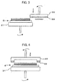
- Fig. 3 shows a method of polishing with polishing cloth 23 cut into a circular shape and pressed against a peripheral portion of SOI wafer from above.
- the SOI wafer 6 is held by a wafer holding table 21 by vacuum suction or the like, and the wafer holding table 21 is rotated by a non-illustrated motor or the like.
- a turn table 22 adhered with the polishing cloth 23 cut into a circular shape is rotated by a non-illustrated motor or the like around an axis perpendicular to the main surface of the SOI wafer 6 as a center.
- the end of the polishing cloth 23 is adjusted so that it should locate at a desired distance from the peripheral end of the SOI wafer 6, i.e., 1-5 mm from the peripheral end.
- polishing is performed with the polishing cloth 23 pressed against the peripheral portion of the SOI wafer 6, while supplying a polishing agent containing colloidal silica and an alkali or an amine as main components to the peripheral portion of the wa
- Fig. 4 shows a polishing method, wherein a turn table 22 formed in a cup-like shape is adhered with a ring-like polishing cloth 23 having an inner periphery (inner diameter) at a distance of 1-5 mm from the peripheral end of the SOI wafer 6, that is, having an inner diameter smaller than the diameter of the base wafer by 2-10 mm and an outer diameter equal to the diameter of the base wafer or larger than it, and polishing is performed by pressing the polishing cloth from above against the peripheral portion of the SOI wafer 6 with aligning the rotation axis of the turn table 22 with that of the SOI wafer 6.
- Fig. 5 shows a polishing method, wherein polishing is performed by pressing an end portion of polishing cloth (buff) 23 cut into a circular shape or having a cylindrical shape with a small thickness against the peripheral portion of the SOI wafer 6 from above or side with rotation around an axis parallel to the main surface of the SOI wafer 6 as a center.
- Fig. 6 shows a polishing method, wherein polishing is performed by pressing polishing cloth (buff) 23 having a cylindrical shape against the peripheral portion of the SOI wafer 6 from above with rotation around an axis parallel to the main surface of the SOI wafer 6 as a center.
- Fig. 7 shows a polishing method, wherein polishing is performed with polishing cloth (buff) 23 having a cylindrical shape and a groove 24 of a desired depth on its side surface by pressing an upper surface of the groove 24 against the peripheral portion of the SOI wafer 6 with rotation of the cylindrical polishing cloth 23 around an axis perpendicular to the main surface of the SOI wafer 6 as a center.
- polishing cloth (buff) 23 having a cylindrical shape and a groove 24 of a desired depth on its side surface by pressing an upper surface of the groove 24 against the peripheral portion of the SOI wafer 6 with rotation of the cylindrical polishing cloth 23 around an axis perpendicular to the main surface of the SOI wafer 6 as a center.
- the polishing cloth may consist of polyurethane foam, nonwoven fabric impregnated with polyurethane or the like, which is usually used for the polishing of silicon wafers.
- the polishing agent is preferably supplied to only the peripheral portion as much as possible. In order to prevent the polishing agent from being brought into contact with portions other than the peripheral portion, it is also possible to supply pure water to the center of the wafer so that the pure water should cover the portions other than the peripheral portion with the aid of centrifugal force.
- the present invention is explained for an SOI wafer that uses two of silicon wafers in which an SOI layer is formed on one of the silicon wafers (base wafer) via an oxide film.
- the present invention is not limited to it, and it can be applied to all bonding wafers produced by the hydrogen ion delamination method.
- an SOI wafer consisting of a silicon wafer (bond wafer) implanted with ions and bonded to an insulator wafer (base wafer) having a different thermal expansion coefficient such as those of quartz, silicon carbide, alumina and so forth
- a thin silicon layer is formed on the insulator wafer.
- a region showing insufficient bonding strength is present in a peripheral portion of the SOI layer after the delamination heat treatment. Therefore, by removing the peripheral portion, specifically, a region of 1-5 mm from the peripheral end of the base wafer, there can be obtained an SOI wafer in which the SOI layer is firmly bonded to the insulator wafer over the whole wafer.
- a thin silicon layer is formed on the silicon wafer.
- the region of insufficient bonding strength in the peripheral portion of the silicon layer can be removed according to the present invention to leave only the portion of the silicon layer firmly bonded to the silicon wafer for the whole wafer.
- the peripheral portion of the thin layer formed on the base wafer can be removed by etching the bonding wafer with masking at least the top surface area other than the peripheral portion to be removed, or etching a plurality of bonding wafers stacked and held in one piece so that at least peripheral portions to be removed should be exposed as described above. Furthermore, the peripheral portion of the thin layer may be removed by polishing only the peripheral portion.
Landscapes
- Mechanical Treatment Of Semiconductor (AREA)
- Element Separation (AREA)
- Weting (AREA)
Applications Claiming Priority (3)
| Application Number | Priority Date | Filing Date | Title |
|---|---|---|---|
| JP29213099 | 1999-10-14 | ||
| JP29213099 | 1999-10-14 | ||
| PCT/JP2000/006795 WO2001027999A1 (fr) | 1999-10-14 | 2000-09-29 | Procede de production de tranches collees et tranche collee |
Publications (3)
| Publication Number | Publication Date |
|---|---|
| EP1170801A1 true EP1170801A1 (de) | 2002-01-09 |
| EP1170801A4 EP1170801A4 (de) | 2003-07-16 |
| EP1170801B1 EP1170801B1 (de) | 2006-07-26 |
Family
ID=17777935
Family Applications (1)
| Application Number | Title | Priority Date | Filing Date |
|---|---|---|---|
| EP00963000A Expired - Lifetime EP1170801B1 (de) | 1999-10-14 | 2000-09-29 | Verbundscheiben-herstellungsmethode |
Country Status (7)
| Country | Link |
|---|---|
| US (1) | US6797632B1 (de) |
| EP (1) | EP1170801B1 (de) |
| JP (1) | JP4277469B2 (de) |
| KR (1) | KR100733112B1 (de) |
| DE (1) | DE60029578T2 (de) |
| TW (1) | TW475215B (de) |
| WO (1) | WO2001027999A1 (de) |
Cited By (7)
| Publication number | Priority date | Publication date | Assignee | Title |
|---|---|---|---|---|
| RU2217842C1 (ru) * | 2003-01-14 | 2003-11-27 | Институт физики полупроводников - Объединенного института физики полупроводников СО РАН | Способ изготовления структуры кремний-на-изоляторе |
| EP1427001A1 (de) * | 2002-12-06 | 2004-06-09 | S.O.I. Tec Silicon on Insulator Technologies S.A. | Verfahren zum Recyceln einer Substratoberfläche mittels lokales Abdünnen |
| US7022586B2 (en) | 2002-12-06 | 2006-04-04 | S.O.I.Tec Silicon On Insulator Technologies S.A. | Method for recycling a substrate |
| EP1845557A3 (de) * | 2006-04-14 | 2008-12-24 | SUMCO Corporation | Substrat-auf-Isolator und Herstellungsverfahren dafür |
| EP1855309A4 (de) * | 2005-02-28 | 2010-11-17 | Shinetsu Handotai Kk | Verfahren zur herstellung eines gebondeten wafers und gebondeter wafer |
| US8298916B2 (en) | 2010-03-02 | 2012-10-30 | Soitec | Process for fabricating a multilayer structure with post-grinding trimming |
| US8330245B2 (en) | 2010-02-25 | 2012-12-11 | Memc Electronic Materials, Inc. | Semiconductor wafers with reduced roll-off and bonded and unbonded SOI structures produced from same |
Families Citing this family (13)
| Publication number | Priority date | Publication date | Assignee | Title |
|---|---|---|---|---|
| US7057234B2 (en) * | 2002-12-06 | 2006-06-06 | Cornell Research Foundation, Inc. | Scalable nano-transistor and memory using back-side trapping |
| FR2852143B1 (fr) * | 2003-03-04 | 2005-10-14 | Soitec Silicon On Insulator | Procede de traitement preventif de la couronne d'une tranche multicouche |
| JP4598413B2 (ja) * | 2004-02-26 | 2010-12-15 | 信越半導体株式会社 | 貼り合わせウエーハの製造方法及び貼り合わせウエーハの酸化膜除去用治具 |
| JP4839818B2 (ja) * | 2005-12-16 | 2011-12-21 | 信越半導体株式会社 | 貼り合わせ基板の製造方法 |
| JP2007243038A (ja) * | 2006-03-10 | 2007-09-20 | Sumco Corp | 貼り合わせウェーハ及びその製造方法 |
| JP2007266352A (ja) * | 2006-03-29 | 2007-10-11 | Disco Abrasive Syst Ltd | ウエーハの加工方法 |
| JP2007317988A (ja) | 2006-05-29 | 2007-12-06 | Shin Etsu Handotai Co Ltd | 貼り合わせウエーハの製造方法 |
| FR2935536B1 (fr) * | 2008-09-02 | 2010-09-24 | Soitec Silicon On Insulator | Procede de detourage progressif |
| JP5478166B2 (ja) * | 2008-09-11 | 2014-04-23 | 株式会社半導体エネルギー研究所 | 半導体装置の作製方法 |
| US20100081251A1 (en) * | 2008-09-29 | 2010-04-01 | Semiconductor Energy Laboratory Co., Ltd. | Method for manufacturing soi substrate |
| JP2010177662A (ja) * | 2009-01-05 | 2010-08-12 | Semiconductor Energy Lab Co Ltd | Soi基板の作製方法及び半導体装置の作製方法 |
| FR2957716B1 (fr) | 2010-03-18 | 2012-10-05 | Soitec Silicon On Insulator | Procede de finition d'un substrat de type semi-conducteur sur isolant |
| JP6715345B2 (ja) | 2016-11-01 | 2020-07-01 | 信越化学工業株式会社 | デバイス層を転写基板に転写する方法 |
Family Cites Families (13)
| Publication number | Priority date | Publication date | Assignee | Title |
|---|---|---|---|---|
| JPS6050970A (ja) | 1983-08-31 | 1985-03-22 | Toshiba Corp | 半導体圧力変換器 |
| JP2604488B2 (ja) | 1989-06-21 | 1997-04-30 | 富士通株式会社 | 接合ウエハおよびその製造方法 |
| JPH0719737B2 (ja) | 1990-02-28 | 1995-03-06 | 信越半導体株式会社 | S01基板の製造方法 |
| JPH0636413B2 (ja) * | 1990-03-29 | 1994-05-11 | 信越半導体株式会社 | 半導体素子形成用基板の製造方法 |
| FR2681472B1 (fr) | 1991-09-18 | 1993-10-29 | Commissariat Energie Atomique | Procede de fabrication de films minces de materiau semiconducteur. |
| JPH0897111A (ja) * | 1994-09-26 | 1996-04-12 | Kyushu Komatsu Denshi Kk | Soi基板の製造方法 |
| US5494849A (en) * | 1995-03-23 | 1996-02-27 | Si Bond L.L.C. | Single-etch stop process for the manufacture of silicon-on-insulator substrates |
| JPH0964321A (ja) * | 1995-08-24 | 1997-03-07 | Komatsu Electron Metals Co Ltd | Soi基板の製造方法 |
| JPH10270298A (ja) | 1997-03-27 | 1998-10-09 | Mitsubishi Materials Shilicon Corp | 張り合わせ基板の製造方法 |
| JP3422225B2 (ja) | 1997-07-08 | 2003-06-30 | 三菱住友シリコン株式会社 | 貼り合わせ半導体基板及びその製造方法 |
| US6265328B1 (en) * | 1998-01-30 | 2001-07-24 | Silicon Genesis Corporation | Wafer edge engineering method and device |
| US6417108B1 (en) * | 1998-02-04 | 2002-07-09 | Canon Kabushiki Kaisha | Semiconductor substrate and method of manufacturing the same |
| JP3932369B2 (ja) * | 1998-04-09 | 2007-06-20 | 信越半導体株式会社 | 剥離ウエーハを再利用する方法および再利用に供されるシリコンウエーハ |
-
2000
- 2000-09-29 KR KR1020017007169A patent/KR100733112B1/ko not_active Expired - Fee Related
- 2000-09-29 WO PCT/JP2000/006795 patent/WO2001027999A1/ja not_active Ceased
- 2000-09-29 US US09/857,569 patent/US6797632B1/en not_active Expired - Lifetime
- 2000-09-29 DE DE60029578T patent/DE60029578T2/de not_active Expired - Lifetime
- 2000-09-29 JP JP2001530119A patent/JP4277469B2/ja not_active Expired - Fee Related
- 2000-09-29 EP EP00963000A patent/EP1170801B1/de not_active Expired - Lifetime
- 2000-10-12 TW TW089121337A patent/TW475215B/zh not_active IP Right Cessation
Cited By (9)
| Publication number | Priority date | Publication date | Assignee | Title |
|---|---|---|---|---|
| EP1427001A1 (de) * | 2002-12-06 | 2004-06-09 | S.O.I. Tec Silicon on Insulator Technologies S.A. | Verfahren zum Recyceln einer Substratoberfläche mittels lokales Abdünnen |
| US7022586B2 (en) | 2002-12-06 | 2006-04-04 | S.O.I.Tec Silicon On Insulator Technologies S.A. | Method for recycling a substrate |
| RU2217842C1 (ru) * | 2003-01-14 | 2003-11-27 | Институт физики полупроводников - Объединенного института физики полупроводников СО РАН | Способ изготовления структуры кремний-на-изоляторе |
| EP1855309A4 (de) * | 2005-02-28 | 2010-11-17 | Shinetsu Handotai Kk | Verfahren zur herstellung eines gebondeten wafers und gebondeter wafer |
| EP1845557A3 (de) * | 2006-04-14 | 2008-12-24 | SUMCO Corporation | Substrat-auf-Isolator und Herstellungsverfahren dafür |
| US7718507B2 (en) | 2006-04-14 | 2010-05-18 | Sumco Corporation | Bonded wafer and method of producing the same |
| US8330245B2 (en) | 2010-02-25 | 2012-12-11 | Memc Electronic Materials, Inc. | Semiconductor wafers with reduced roll-off and bonded and unbonded SOI structures produced from same |
| US8440541B2 (en) | 2010-02-25 | 2013-05-14 | Memc Electronic Materials, Inc. | Methods for reducing the width of the unbonded region in SOI structures |
| US8298916B2 (en) | 2010-03-02 | 2012-10-30 | Soitec | Process for fabricating a multilayer structure with post-grinding trimming |
Also Published As
| Publication number | Publication date |
|---|---|
| EP1170801A4 (de) | 2003-07-16 |
| TW475215B (en) | 2002-02-01 |
| JP4277469B2 (ja) | 2009-06-10 |
| US6797632B1 (en) | 2004-09-28 |
| KR100733112B1 (ko) | 2007-06-27 |
| EP1170801B1 (de) | 2006-07-26 |
| DE60029578T2 (de) | 2007-07-26 |
| KR20010101155A (ko) | 2001-11-14 |
| DE60029578D1 (de) | 2006-09-07 |
| WO2001027999A1 (fr) | 2001-04-19 |
Similar Documents
| Publication | Publication Date | Title |
|---|---|---|
| US6797632B1 (en) | Bonded wafer producing method and bonded wafer | |
| US6720640B2 (en) | Method for reclaiming delaminated wafer and reclaimed delaminated wafer | |
| KR101151458B1 (ko) | 접합 웨이퍼의 제조방법 및 접합 웨이퍼 | |
| US7855129B2 (en) | Method for manufacturing direct bonded SOI wafer and direct bonded SOI wafer manufactured by the method | |
| KR100789205B1 (ko) | 실리콘 웨이퍼 및 에스오아이 웨이퍼의 제조방법, 그리고그 에스오아이 웨이퍼 | |
| CN101331585B (zh) | 贴合基板的制造方法 | |
| KR100327840B1 (ko) | Soi기판의 재생방법 및 재생기판 | |
| EP0854500B1 (de) | Verfahren zur Herstellung eines geklebten Substrates | |
| US20030008478A1 (en) | Production method for silicon wafer and soi wafer, and soi wafer | |
| JPWO2001027999A1 (ja) | 貼り合わせウエーハの製造方法及び貼り合わせウエーハ | |
| US20070114609A1 (en) | Semiconductor substrate and method of manufacturing the same | |
| US6900113B2 (en) | Method for producing bonded wafer and bonded wafer | |
| WO2001048825A1 (en) | Method for manufacturing bonded wafer | |
| US5918139A (en) | Method of manufacturing a bonding substrate | |
| JPH0745485A (ja) | 接着半導体基板の製造方法 | |
| JP2006270039A (ja) | 貼り合わせウエーハの製造方法及び貼り合わせウエーハ | |
| JP4581349B2 (ja) | 貼合せsoiウェーハの製造方法 | |
| JP3945130B2 (ja) | 張り合わせ誘電体分離ウェーハの製造方法 | |
| JP2004022838A (ja) | 貼り合わせsoi基板およびその製造方法 | |
| JP3524009B2 (ja) | Soiウェーハおよびその製造方法 | |
| JPH1187203A (ja) | 基板の貼り合わせ方法 |
Legal Events
| Date | Code | Title | Description |
|---|---|---|---|
| PUAI | Public reference made under article 153(3) epc to a published international application that has entered the european phase |
Free format text: ORIGINAL CODE: 0009012 |
|
| 17P | Request for examination filed |
Effective date: 20010628 |
|
| AK | Designated contracting states |
Kind code of ref document: A1 Designated state(s): AT BE CH CY DE DK ES FI FR GB GR IE IT LI LU MC NL PT SE |
|
| A4 | Supplementary search report drawn up and despatched |
Effective date: 20030530 |
|
| RIC1 | Information provided on ipc code assigned before grant |
Ipc: 7H 01L 21/762 B Ipc: 7H 01L 27/12 A |
|
| 17Q | First examination report despatched |
Effective date: 20030821 |
|
| RBV | Designated contracting states (corrected) |
Designated state(s): DE FR GB |
|
| RTI1 | Title (correction) |
Free format text: BONDED WAFER PRODUCING METHOD |
|
| GRAP | Despatch of communication of intention to grant a patent |
Free format text: ORIGINAL CODE: EPIDOSNIGR1 |
|
| GRAS | Grant fee paid |
Free format text: ORIGINAL CODE: EPIDOSNIGR3 |
|
| GRAA | (expected) grant |
Free format text: ORIGINAL CODE: 0009210 |
|
| AK | Designated contracting states |
Kind code of ref document: B1 Designated state(s): DE FR GB |
|
| REG | Reference to a national code |
Ref country code: GB Ref legal event code: FG4D |
|
| REF | Corresponds to: |
Ref document number: 60029578 Country of ref document: DE Date of ref document: 20060907 Kind code of ref document: P |
|
| ET | Fr: translation filed | ||
| PLBE | No opposition filed within time limit |
Free format text: ORIGINAL CODE: 0009261 |
|
| STAA | Information on the status of an ep patent application or granted ep patent |
Free format text: STATUS: NO OPPOSITION FILED WITHIN TIME LIMIT |
|
| 26N | No opposition filed |
Effective date: 20070427 |
|
| PGFP | Annual fee paid to national office [announced via postgrant information from national office to epo] |
Ref country code: GB Payment date: 20081001 Year of fee payment: 9 |
|
| GBPC | Gb: european patent ceased through non-payment of renewal fee |
Effective date: 20090929 |
|
| PG25 | Lapsed in a contracting state [announced via postgrant information from national office to epo] |
Ref country code: GB Free format text: LAPSE BECAUSE OF NON-PAYMENT OF DUE FEES Effective date: 20090929 |
|
| REG | Reference to a national code |
Ref country code: FR Ref legal event code: PLFP Year of fee payment: 17 |
|
| REG | Reference to a national code |
Ref country code: FR Ref legal event code: PLFP Year of fee payment: 18 |
|
| REG | Reference to a national code |
Ref country code: FR Ref legal event code: PLFP Year of fee payment: 19 |
|
| PGFP | Annual fee paid to national office [announced via postgrant information from national office to epo] |
Ref country code: FR Payment date: 20190815 Year of fee payment: 20 Ref country code: DE Payment date: 20190917 Year of fee payment: 20 |
|
| REG | Reference to a national code |
Ref country code: DE Ref legal event code: R071 Ref document number: 60029578 Country of ref document: DE |