EP1178543A1 - Dispositif semi-conducteur émetteur de lumière - Google Patents
Dispositif semi-conducteur émetteur de lumière Download PDFInfo
- Publication number
- EP1178543A1 EP1178543A1 EP01115378A EP01115378A EP1178543A1 EP 1178543 A1 EP1178543 A1 EP 1178543A1 EP 01115378 A EP01115378 A EP 01115378A EP 01115378 A EP01115378 A EP 01115378A EP 1178543 A1 EP1178543 A1 EP 1178543A1
- Authority
- EP
- European Patent Office
- Prior art keywords
- layer
- active layer
- semiconductor
- type
- zno
- Prior art date
- Legal status (The legal status is an assumption and is not a legal conclusion. Google has not performed a legal analysis and makes no representation as to the accuracy of the status listed.)
- Withdrawn
Links
- 239000004065 semiconductor Substances 0.000 title claims abstract description 138
- 150000001875 compounds Chemical class 0.000 claims abstract description 61
- 239000000463 material Substances 0.000 claims abstract description 18
- 239000000758 substrate Substances 0.000 claims description 29
- 239000000203 mixture Substances 0.000 claims description 20
- 238000003475 lamination Methods 0.000 claims description 12
- 229910052725 zinc Inorganic materials 0.000 claims description 12
- 229910021476 group 6 element Inorganic materials 0.000 claims description 11
- 229910052760 oxygen Inorganic materials 0.000 claims description 10
- -1 nitride compound Chemical class 0.000 claims description 9
- 229910052711 selenium Inorganic materials 0.000 claims description 9
- 229910052717 sulfur Inorganic materials 0.000 claims description 8
- 238000005530 etching Methods 0.000 claims description 7
- 229910052749 magnesium Inorganic materials 0.000 claims description 6
- 239000004020 conductor Substances 0.000 claims description 2
- 239000013078 crystal Substances 0.000 abstract description 32
- 238000010276 construction Methods 0.000 abstract description 14
- 230000007547 defect Effects 0.000 abstract description 3
- 239000011701 zinc Substances 0.000 description 22
- 229910002601 GaN Inorganic materials 0.000 description 21
- 239000011669 selenium Substances 0.000 description 19
- 239000011777 magnesium Substances 0.000 description 13
- JMASRVWKEDWRBT-UHFFFAOYSA-N Gallium nitride Chemical compound [Ga]#N JMASRVWKEDWRBT-UHFFFAOYSA-N 0.000 description 12
- 239000007789 gas Substances 0.000 description 8
- 238000000034 method Methods 0.000 description 7
- 229910052594 sapphire Inorganic materials 0.000 description 7
- 239000010980 sapphire Substances 0.000 description 7
- 239000002019 doping agent Substances 0.000 description 6
- 238000004519 manufacturing process Methods 0.000 description 6
- LJSQFQKUNVCTIA-UHFFFAOYSA-N diethyl sulfide Chemical compound CCSCC LJSQFQKUNVCTIA-UHFFFAOYSA-N 0.000 description 4
- 238000002488 metal-organic chemical vapour deposition Methods 0.000 description 4
- 238000001451 molecular beam epitaxy Methods 0.000 description 4
- 238000007738 vacuum evaporation Methods 0.000 description 4
- 238000001039 wet etching Methods 0.000 description 4
- HEMHJVSKTPXQMS-UHFFFAOYSA-M Sodium hydroxide Chemical compound [OH-].[Na+] HEMHJVSKTPXQMS-UHFFFAOYSA-M 0.000 description 3
- HSFWRNGVRCDJHI-UHFFFAOYSA-N alpha-acetylene Natural products C#C HSFWRNGVRCDJHI-UHFFFAOYSA-N 0.000 description 3
- 229910021478 group 5 element Inorganic materials 0.000 description 3
- 230000003287 optical effect Effects 0.000 description 3
- IJGRMHOSHXDMSA-UHFFFAOYSA-N Atomic nitrogen Chemical compound N#N IJGRMHOSHXDMSA-UHFFFAOYSA-N 0.000 description 2
- XUIMIQQOPSSXEZ-UHFFFAOYSA-N Silicon Chemical compound [Si] XUIMIQQOPSSXEZ-UHFFFAOYSA-N 0.000 description 2
- WYURNTSHIVDZCO-UHFFFAOYSA-N Tetrahydrofuran Chemical compound C1CCOC1 WYURNTSHIVDZCO-UHFFFAOYSA-N 0.000 description 2
- 229910052785 arsenic Inorganic materials 0.000 description 2
- 230000004888 barrier function Effects 0.000 description 2
- 230000000903 blocking effect Effects 0.000 description 2
- 229910052793 cadmium Inorganic materials 0.000 description 2
- 239000000969 carrier Substances 0.000 description 2
- ALCDAWARCQFJBA-UHFFFAOYSA-N ethylselanylethane Chemical compound CC[Se]CC ALCDAWARCQFJBA-UHFFFAOYSA-N 0.000 description 2
- 238000010030 laminating Methods 0.000 description 2
- 229910052757 nitrogen Inorganic materials 0.000 description 2
- 229910052698 phosphorus Inorganic materials 0.000 description 2
- SBIBMFFZSBJNJF-UHFFFAOYSA-N selenium;zinc Chemical compound [Se]=[Zn] SBIBMFFZSBJNJF-UHFFFAOYSA-N 0.000 description 2
- 229910052710 silicon Inorganic materials 0.000 description 2
- 239000010703 silicon Substances 0.000 description 2
- 231100000701 toxic element Toxicity 0.000 description 2
- JLTRXTDYQLMHGR-UHFFFAOYSA-N trimethylaluminium Chemical compound C[Al](C)C JLTRXTDYQLMHGR-UHFFFAOYSA-N 0.000 description 2
- 229910002704 AlGaN Inorganic materials 0.000 description 1
- OKTJSMMVPCPJKN-UHFFFAOYSA-N Carbon Chemical compound [C] OKTJSMMVPCPJKN-UHFFFAOYSA-N 0.000 description 1
- UFHFLCQGNIYNRP-UHFFFAOYSA-N Hydrogen Chemical compound [H][H] UFHFLCQGNIYNRP-UHFFFAOYSA-N 0.000 description 1
- 241000951490 Hylocharis chrysura Species 0.000 description 1
- 239000012670 alkaline solution Substances 0.000 description 1
- 229910052782 aluminium Inorganic materials 0.000 description 1
- QVGXLLKOCUKJST-UHFFFAOYSA-N atomic oxygen Chemical compound [O] QVGXLLKOCUKJST-UHFFFAOYSA-N 0.000 description 1
- 230000005540 biological transmission Effects 0.000 description 1
- 230000015572 biosynthetic process Effects 0.000 description 1
- 229910052799 carbon Inorganic materials 0.000 description 1
- 238000003763 carbonization Methods 0.000 description 1
- 239000012159 carrier gas Substances 0.000 description 1
- 238000005229 chemical vapour deposition Methods 0.000 description 1
- BUMGIEFFCMBQDG-UHFFFAOYSA-N dichlorosilicon Chemical compound Cl[Si]Cl BUMGIEFFCMBQDG-UHFFFAOYSA-N 0.000 description 1
- AXAZMDOAUQTMOW-UHFFFAOYSA-N dimethylzinc Chemical compound C[Zn]C AXAZMDOAUQTMOW-UHFFFAOYSA-N 0.000 description 1
- 238000001312 dry etching Methods 0.000 description 1
- 230000000694 effects Effects 0.000 description 1
- 125000002534 ethynyl group Chemical group [H]C#C* 0.000 description 1
- 239000003574 free electron Substances 0.000 description 1
- 229910052737 gold Inorganic materials 0.000 description 1
- 231100000086 high toxicity Toxicity 0.000 description 1
- 229910052739 hydrogen Inorganic materials 0.000 description 1
- 239000001257 hydrogen Substances 0.000 description 1
- 239000012535 impurity Substances 0.000 description 1
- 229910052738 indium Inorganic materials 0.000 description 1
- 239000011810 insulating material Substances 0.000 description 1
- 238000012423 maintenance Methods 0.000 description 1
- 229910052751 metal Inorganic materials 0.000 description 1
- 239000002184 metal Substances 0.000 description 1
- 150000004767 nitrides Chemical class 0.000 description 1
- 239000001301 oxygen Substances 0.000 description 1
- 238000000059 patterning Methods 0.000 description 1
- 230000035484 reaction time Effects 0.000 description 1
- 230000006798 recombination Effects 0.000 description 1
- 238000005215 recombination Methods 0.000 description 1
- 230000002040 relaxant effect Effects 0.000 description 1
- 239000000126 substance Substances 0.000 description 1
- YLQBMQCUIZJEEH-UHFFFAOYSA-N tetrahydrofuran Natural products C=1C=COC=1 YLQBMQCUIZJEEH-UHFFFAOYSA-N 0.000 description 1
- 125000003718 tetrahydrofuranyl group Chemical group 0.000 description 1
- 238000002230 thermal chemical vapour deposition Methods 0.000 description 1
- 231100000331 toxic Toxicity 0.000 description 1
- 230000002588 toxic effect Effects 0.000 description 1
- 239000012808 vapor phase Substances 0.000 description 1
- XLOMVQKBTHCTTD-UHFFFAOYSA-N zinc oxide Inorganic materials [Zn]=O XLOMVQKBTHCTTD-UHFFFAOYSA-N 0.000 description 1
- IPSRAFUHLHIWAR-UHFFFAOYSA-N zinc;ethane Chemical compound [Zn+2].[CH2-]C.[CH2-]C IPSRAFUHLHIWAR-UHFFFAOYSA-N 0.000 description 1
Images


Classifications
-
- H—ELECTRICITY
- H10—SEMICONDUCTOR DEVICES; ELECTRIC SOLID-STATE DEVICES NOT OTHERWISE PROVIDED FOR
- H10H—INORGANIC LIGHT-EMITTING SEMICONDUCTOR DEVICES HAVING POTENTIAL BARRIERS
- H10H20/00—Individual inorganic light-emitting semiconductor devices having potential barriers, e.g. light-emitting diodes [LED]
- H10H20/80—Constructional details
- H10H20/81—Bodies
- H10H20/822—Materials of the light-emitting regions
- H10H20/823—Materials of the light-emitting regions comprising only Group II-VI materials, e.g. ZnO
-
- H—ELECTRICITY
- H10—SEMICONDUCTOR DEVICES; ELECTRIC SOLID-STATE DEVICES NOT OTHERWISE PROVIDED FOR
- H10H—INORGANIC LIGHT-EMITTING SEMICONDUCTOR DEVICES HAVING POTENTIAL BARRIERS
- H10H20/00—Individual inorganic light-emitting semiconductor devices having potential barriers, e.g. light-emitting diodes [LED]
- H10H20/80—Constructional details
- H10H20/81—Bodies
- H10H20/822—Materials of the light-emitting regions
-
- H—ELECTRICITY
- H01—ELECTRIC ELEMENTS
- H01S—DEVICES USING THE PROCESS OF LIGHT AMPLIFICATION BY STIMULATED EMISSION OF RADIATION [LASER] TO AMPLIFY OR GENERATE LIGHT; DEVICES USING STIMULATED EMISSION OF ELECTROMAGNETIC RADIATION IN WAVE RANGES OTHER THAN OPTICAL
- H01S5/00—Semiconductor lasers
- H01S5/30—Structure or shape of the active region; Materials used for the active region
- H01S5/32—Structure or shape of the active region; Materials used for the active region comprising PN junctions, e.g. hetero- or double- heterostructures
- H01S5/327—Structure or shape of the active region; Materials used for the active region comprising PN junctions, e.g. hetero- or double- heterostructures in AIIBVI compounds, e.g. ZnCdSe-laser
Definitions
- the present invention relates to a semiconductor light emitting device which emits light even with a short wavelength of a blue-band color ranging from ultraviolet to yellow, such as a light emitting diode (hereinafter abbreviated as LED) used in a light source including a full-color display or a signal light, or a semiconductor laser (hereinafter abbreviated as LD) used in a next-generation high-definition DVD light source which continuously oscillates at a room temperature. More particularly, the present invention relates to a semiconductor light emitting device having an active layer made of ZnO-based compound semiconductor which has a narrowed band gap and excellent crystallinity.
- a blue type (which hereinafter means a color band of ultraviolet to near-yellow) LED or LD can be obtained by laminating GaN-based compound semiconductor layers on a sapphire substrate, thus attracting the attention.
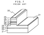
- This sort of a conventional blue type semiconductor light emitting device is made, as shown for example in FIG.
- MOCVD Metal Organic Chemical Vapor Deposition
- laminated semiconductor layers are, as shown in FIG. 7, partially etched by dry-etching or the like to expose the n-type contact layer 23, and an n-side electrode 31 and a p-side electrode 30 are provided on the surfaces of the n-type contact layer 23 and the p-type contact layer 29, respectively.
- a ZnO-based compound semiconductor has its exciton (pair of an electron and a hole bound by the Coulomb force) having a very large combination energy (binding energy) of 60 meV, which is larger than the heat energy at room temperature of 26 meV, so that the exciton can exist in a stable manner even at room temperature.
- This exciton once formed, generates a photon easily. That is, it emits light effectively. Accordingly, it is known that the exciton will emit light much more effectively than emission by direct recombination, by which a free electron and a free hole are directly recombined with each other. This has led to a research of a semiconductor light emitting device made of ZnO-based compound semiconductor.
- the ZnO compound however, has a band gap of 3.2 eV, so that when it is used as is to form an active layer, light can be emitted only in the vicinity of 370, nm in an ultraviolet region of wavelengths.
- the material As a light source for a high-definition DVD, for example, it must meet the two requirements of a transmission factor of an optical disk substrate and a recording density on the disk, so that the wavelength of that light source must be in a range of 400-430 nm.
- the band gap of ZnO must be narrowed and therefore it is discussed to mix a CdO crystal into a ZnO crystal in order to narrow the band gap in a prior art ZnO-based compound semiconductor, and to use a CdZnO-based compound ("CdZnO-based" means that the crystal mixture ratio of Cd and Zn is variable) as a material of an active layer.
- CdZnO-based means that the crystal mixture ratio of Cd and Zn is variable
- the group III nitride compound semiconductor (gallium nitride based compound semiconductor) used for such a blue type semiconductor light emitting device which has a short wavelength is very stable thermally and chemically and also highly reliable, being excellent in a long life.
- the semiconductor must be grown at a high temperature of 1000 °C or so in order to form a semiconductor layer excellent in crystallinity.
- a semiconductor layer such as an active layer containing In, on the other hand, is difficult to mix element In and GaN and also the element In has a high vapor pressure, so that to contain a sufficient quantity of In, the layer can be grown only at about 700 °C or lower. This property of In disables growing at a high temperature required for making a semiconductor layer excellent in crystallinity to thereby prevent it from forming the excellent layer in crystallinity, thus leading to problems of the deteriorated light emitting efficiency and the shortened life.
- a CdZnO-based compound may possibly be employed but Cd is highly toxic, so that any other materials with better safety are desired.
- Another object of the present invention is to provide a blue type emitting semiconductor laser which can be used as a high-definition DVD light source.
- the inventors greatly investigated to obtain a semiconductor light emitting device mainly made of ZnO-based compound by narrowing their band gap without using Cd and found as a result that by replacing O of ZnO partially with any other group VI element such as S or Se in growth, such a mixed crystal as ZnO 1-x S x (0 ⁇ x ⁇ 1) or ZnO 1-y Se y (0 ⁇ y ⁇ 1) can be formed and also that by utilizing a band gap bowing phenomenon at the time of crystal mixture, the band gap can be narrowed to a desired range.
- a ZnO-based compound refers to a compound containing at least Zn and O in which Zn is replaced partially with a group II element such as Mg or Cd and/or a compound in which O is replaced partially with any other group VI element such as s or Se.
- a mixed crystal with a finely controlled crystal mixture rate has such a property that its band gap changes in bowing (i.e., in a bow shape or parabola shape), so that by finely controlling the crystal mixture ratio at a portion where the band gap changes in bowing, a desired band gap can be obtained.
- the crystal mixture ratio x of S is preferably 0.02-0.1 and more preferably 0.03-0.06, while the crystal mixture ratio y of Se is preferably 0.005-0.1 and more preferably 0.008-0.04, thus being well suited for the above-mentioned application.
- the semiconductor light emitting device comprises an active layer for emitting light when a current injected thereto and n-type and p-type clad layers which are made of a material having a larger band gap than the active layer and which sandwich the active layer between both faces thereof, in which the active layer is formed of a compound semiconductor containing Zn, O, and at least one of other group VI elements than O.
- This construction makes it possible to narrow the band gap than in a case of using ZnO and control over the crystal mixture ratio of group VI element other than O makes it possible to obtain a semiconductor layer with good crystallinity of its active layer having a band gap for emitting light of a desired wavelength, thus obtaining a semiconductor light emitting device with a high light emitting efficiency. It is also possible to mix a group VI element other than O in a mixed crystal compound in which Zn of ZnO is partially replaced with Cd or Mg. In this case, Cd acts to narrow the band gap and Mg acts to widen it, so that the desirable crystal mixture rate is shifted from the above-mentioned x and y values.
- the above-mentioned clad layer may be formed of an oxide compound containing Zn, an oxide compound semiconductor containing Mg and Zn, or a group III nitride compound semiconductor, while the above-mentioned active layer may be formed of ZnO 1-x S x (0 ⁇ x ⁇ 1) or ZnO 1-y Se y (0 ⁇ y ⁇ 1). That is, even in the case of a semiconductor light emitting device made of a group III nitride compound semiconductor, although its active layer does not have good crystallinity as mentioned above but it is possible to use a compound semiconductor containing Zn, O, and a group VI element other than O according to the present invention only in that active layer.
- a group III nitride compound semiconductor also called a gallium nitride based compound semiconductor
- a group III nitride compound semiconductor also called a gallium nitride based compound semiconductor
- a group III nitride compound semiconductor refers to a semiconductor made of a compound of a group III element Ga and a group V element N, or a compound in which a part or the whole of a group III element Ga is replaced with another group III element such as Al or In, and/or a compound in which a part of a group V element N is replaced with another group V element such as P or As.
- the above-mentioned active layer may be a semiconductor layer containing ZnO, O, S, and Se.
- the above-mentioned active layer may be formed of a bulk layer made of ZnO 1-x S x or ZnO 1-y Se y , or a quantum well structure obtaining by modifying the composition of ZnO 1-x S x or ZnO 1- y Se y .
- the bulk layer here refers to a one that its active layer as a whole has a uniform composition.
- the above-mentioned active layer may have light guide layers on its both sides.
- the structure for defining a current injecting region in the active layer may be of an electrode stripe type in which an electrode provided on the surface of a semiconductor lamination is formed in a stripe, or a mesa stripe type in which a mesa type shape is formed from the surface of a semiconductor lamination to part of an upper side clad layer, or a SAS type in which a current restricting layer having a stripe groove is formed in either one of clad layers of a semiconductor lamination.
- the substrate on which a semiconductor lamination including the above-mentioned n-type clad layer, the active layer, and the p-type clad layer is formed is electrically conductive, one electrode of the two can be formed on the back side of the substrate, thus facilitating the manufacturing processes and also obtaining a vertical type device.
- conductive includes the semiconductor in which the series resistance matters little.
- a semiconductor light emitting device has such a configuration that an active layer 5 for emitting light when a current is injected thereto is sandwiched between an n-type clad layer 4 and a p-type clad layer 6 made of a material having a lager band gap than that of the active layer 5, in which the above-mentioned active layer 5 is made of a compound semiconductor containing Zn, O, and a group VI element other than O.
- the active layer 5 emits light when carriers are recombined and its band gap determines a wavelength of the light emitted, so that it is made of a material of the band gap corresponding to a desired value of the wavelength, and is formed in a thickness of 0.1 ⁇ m or so by e.g. a bulk layer.
- gallium nitride based compound semiconductor has been employed in a prior art blue type semiconductor light emitting device in which an active layer is sandwiched between clad layers having a larger band gap than that of the clad layer and the active layer has been made of an InGaN-based (which means that a crystal mixture ratio of In can be changed so as to provide a desired band gap) compound semiconductor.
- the InGaN-based compound semiconductor has poor crystallinity and cannot set the crystal mixture ratio of In at a constant level or higher and so is not able to emit light having a long wavelength of a certain value or larger.
- ZnO-based compound semiconductor it is necessary to mix a Cd crystal in order to narrow the band gap, thus giving rise to a problem of high toxicity.
- a group VI element other than O such as S or Se
- the band gap can be adjusted in the desired value by using the bowing phenomenon at the time of growing the mixed crystal to thereby narrow the band gap to a desired range.
- the electronegativity of As is 2.0 and that of P is 2.1, so that InGaAsP has a smaller value of c, in which case therefore the bowing phenomenon occurs scarcely even if the crystal mixture ratio between As and P is changed, whereas the electronegativity of O is 3.5 and those of S and Se are 2.5 and 2.4 respectively and so have a large difference with respect to that of O, so that ZnOS or ZnOSe gives the bowing phenomenon remarkably.
- This change in band gap in indicated in the graph of FIG. 6.
- a desired band gap can be obtained by forming a mixed crystal compound such as ZnOS or ZnOSe.
- this active layer 5 can be provided with a desired band gap as far as it contains Zn, O, and other group VI element as mentioned above, Zn may be replaced with any other group II type element, or it may contain two or more group VI type elements other than O such as S and Se. Also, it may of course contain such dopant elements as Al or N.
- the crystal mixture ratio x of S in the active layer 5 expressed as ZnO 1-x S x or ZnO 1-y Se y is preferably 0.02-0.1 and more preferably 0.03-0.06, while the crystal mixture ratio y of Se is preferably 0.005-0.1 and more preferably 0.008-0.04.
- the crystal mixture ratio x and y can be on the side of nearly 0 but also be on the side opposite of the parabola with respect to its minimal point (where x and y take on a larger value) in order to obtain a desired band gap.
- the clad layers 4 and 6 only have to have a larger band gap than the active layer 5 to thereby confine carriers in therein effectively and so may be made of any other group III nitride compound (gallium nitride based compound semiconductor) as far as it gives that confinement effect.
- Mg z Zn 1-z O can be used to enable wet etching unlike by a gallium nitride based compound semiconductor and so is preferably in manufacturing of an LD described later because it facilitates constructing a mesa shape or incorporating an internal current restricting layer.
- This n-type clad layer 4 is formed to a thickness of, e.g. 2 ⁇ m or so and the p-type clad layer 6, e.g. 0.5 ⁇ m or so.
- the substrate 1 is made of, e.g. sapphire, it is possible to use a GaN substrate, a silicon substrate on which SiC is formed, or mono-crystal SiC substrate also in a case where the clad layer is formed of a gallium nitride based compound semiconductor.
- a buffer layer 2 made of, e.g. ZnO, for relaxing lattice mismatching in the compound semiconductor.
- This buffer layer 2 may be of a non-doped type or of the other conductivity type as far as the substrate 1 is made of an insulating material such as sapphire.
- the buffer layer 2 is formed to have the same conductivity type as that of the substrate 1. Thereon is formed an n-type contact layer 3 made of ZnO to a thickness of 1-2 ⁇ m or so.
- the substrate 1 is set in, e.g. an MOCVD apparatus and heated to 300-600 °C or so to then act in a vapor phase with a necessary dopant gas introduced together with a carrier gas H 2 in order to grow a semiconductor layer, so that by changing the reactive gas sequentially or changing its flow rate, it is possible to laminate semiconductor layers at a desired crystal mixture ratio.
- TMA trimethyl-aluminium
- the clad layers and so on other than the active layer can be formed of group III nitride compound such as, GaN-based or AlGaN-based compound.
- group III nitride compound semiconductor layers can be grown at about 1000 °C and the active layer can be grown at the above-mentioned temperature of 600 °C to grow all the layers with good crystallinity.
- an MBE Molecular Beam Epitaxy
- the sapphire substrate 1 is set in, e.g. an MBE apparatus and heated to 300-600 °C or so to then grow the layers by opening the shutters of necessary material sources such as a Zn source (cell), an Mg source, a plasma oxygen source, S or Se source, an Al source as a dopant, a plasma nitrogen source, or the like.
- necessary material sources such as a Zn source (cell), an Mg source, a plasma oxygen source, S or Se source, an Al source as a dopant, a plasma nitrogen source, or the like.
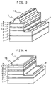
- FIG. 2 is a perspective view for explaining an electrode stripe-type LD chip of another embodiment of the semiconductor light emitting device according to the present invention.
- This LD chip also has the same construction as that of the LED chip of FIG. 1 except mainly that to provide an LD, light guide layers 14 and 16 are provided between the active layer 15 and each of the clad layers and also that the active layer 15 is formed in a quantum well structure.
- the buffer layer 2 made of ZnO to a thickness of 0.1 ⁇ m or so, on which is formed the n-type contact layer 3 made of ZnO to a thickness of 1 ⁇ m or so.
- the active layer 15 is formed in a multiple-quantum well structure which laminates therein barrier layers and well layers made of, e.g. non-doped ZnO 0.95 S 0.05 /ZnO 0.98-1.0 S 0.02-0 to thicknesses of 5 nm and 4 nm respectively two through 5 layers each.
- barrier layers and well layers made of, e.g. non-doped ZnO 0.95 S 0.05 /ZnO 0.98-1.0 S 0.02-0 to thicknesses of 5 nm and 4 nm respectively two through 5 layers each.
- ZnOSe ZnOSe is used to form the active layer
- the same combination of the barrier and well layers can be used which are made of ZnO 0.97 Se 0.03 /ZnO 0.9-1.0 Se 0.1-0 .
- the n-side electrode 9 made of Ti/Au
- the p-side electrode 10 made of, e.g., Ni/Al/Au.
- the p-side electrode 10 formed in a stripe with a width of, e.g. 10 ⁇ m or so is directly formed on the p-type contact layer 7.
- the semiconductor layers to be laminated one on another are made of a semiconductor oxide
- the active layer is improved in crystallinity and can be easily etched to enable wet etching, so that even when the substrate is made of sapphire and so cannot easily be cleaved, the light emitting face of the end face of the active layer can be easily formed in a flat face, thus making it possible to easily form a good resonator.
- FIG. 3 is a perspective view for explaining the LD chip of a further embodiment of the semiconductor light emitting device of the present invention.
- This embodiment employs a mesa stripe-type construction in which instead of a stripe only of the p-side electrode 10, a part of the p-type clad layer 6 is also etched off in a mesa shape, in which case this mesa-type etching is achieved only by re-forming the mask at the same time as performing etching to expose the n-type contact layer 3.
- the lamination structure of the other semiconductor layers is the same as that shown in FIG. 2, with the same manufacturing method employed also.
- FIG. 4 is a similar perspective view for explaining the LD chip of a still further embodiment of the semiconductor light emitting device of the present invention.
- This embodiment exemplifies an SAS-type construction in which an n-type current restricting layer (internal current blocking layer) 17 on the side of the p-type clad layer 6.
- an n-type current restricting layer internal current blocking layer 17 on the side of the p-type clad layer 6.
- the buffer layer 2 the n-type contact layer 3
- the n-type clad layer 4 the n-type light guide layer 14, the active layer 15, the p-type light guide layer 16, and the p-type clad layer 6 in this order, on which is then grown the current restricting layer 17 made of , e.g. n-type Mg 0.2 Zn 0.8 O, to a thickness of 0.4 ⁇ m or so.
- the relevant wafer is once taken out from the growing apparatus, to deposit a resist film on the surface and pattern it into a stripe shape, thus etching the current restricting layer 17 using an alkaline solution such as NaOH into a stripe shape to then form the stripe groove 18.
- the wafer is put back into the MOCVD apparatus to grow the p-type contact layer 7 made of p-type ZnO in the same way as the above-mentioned example.
- the n-side electrode 9 and the p-side electrode 10 are formed to provide a chip, thus giving an LD chip having such a construction as shown in FIG. 4.
- the p-type clad layer 6 may be made in two stages in construction, to form the current restricting layer 17 therebetween.
- the lamination structure employing a gallium nitride based compound semiconductor is, as mentioned above, resistant against chemicals, it has been impossible to etch off such semiconductor layers as laminated in this embodiment to form a stripe groove, thus disabling sufficiently concentrating current paths up to the vicinity of the active layer, to guard against which, however, ZnO-based compound can be used to thereby incorporate into semiconductor layers a current restricting layer (internal current blocking layer) 17 having such a stripe groove formed therein.
- FIG. 5 is a similar perspective view for explaining an still further embodiment of the LD chip of the semiconductor light emitting device according to the present invention.
- the substrate is made of a conductive material in place of sapphire and, as a result, has the n-side electrode 9 provided on a back side of the substrate 11.
- a silicon (Si) substrate 11 on the surface of which is formed a cubic-crystal SiC layer 12, on which surface are laminated the above-mentioned semiconductor layers directly or via a buffer layer not shown.
- This SiC layer 12 is specifically formed by, for example, holding the Si substrate 11, for carbonization, in an atmosphere containing acetylene (C 2 H 2 ) and hydrogen at about 1020 °C for 60 minutes or so to thereby form a SiC film, not shown, to a thickness of 10 nm or so and then by introducing dichloro-silane (SiH 2 Cl 2 ), which is a Si source gas, and C 2 H 2 , which is a carbon source gas, in the same furnace to thereby grow the SiC film to a thickness of, e.g. 2 ⁇ m or so by thermal CVD method. Afterward, the semiconductor layers are laminated almost the same way as above.
- the etching-free construction employed in this embodiment since the semiconductor layer lamination need not be grown at such a high temperature as required for a gallium nitride based compound semiconductor, then they can be grown at a low temperature of 600 °C or lower to thereby greatly mitigate the loads on the growing apparatus, thus facilitating its maintenance and the processes for growing the semiconductor layers. Further, that construction gives excellent crystallinity to the active layer, thus making it possible to obtain an LD and an LED having a good light emitting efficiency.
- any construction of the above-mentioned embodiments including a current-restricting layer incorporating construction may be employed to thereby use the above-mentioned conductive substrate so that both the p-side and n-side electrodes may be taken out from the upper and back sides of the chip, thus providing such a device that is very easy to handle in, e.g. die bonding.
- a conductive substrate may be made of, besides a SiC crystal, GaN so that oxide semiconductor layers may be laminated thereon likewise.
- the active layer of LD is used a multiple-quantum well structure as the active layer of LD, it may be formed in a single-quantum well structure or a bulk structure. Further, as far as the active layer can form light guide layer sufficiently, of course no separate light guide layer need to be provided thereon. Note here that in the figures showing the above-mentioned embodiments, the substrates 1 and 11 are a few tens of times as thick as the other layers but are shown much thinner. Also the thickness of the other semiconductor layers is not shown as it is.
- the band gap of ZnO can be narrowed without using a toxic element such as Cd, it is possible to provide a ZnO-based oxide semiconductor with a band gap ranging from ultraviolet to light having a wavelength of 400-430 nm required for a light source of a high-definition DVD, thus advantageously using a short-wavelength semiconductor light emitting device.
- the semiconductor light emitting device employs a structure in which the active layer is made of a ZnO-based compound semiconductor and sandwiched by the clad layers, its crystallinity is not deteriorated unlike an InGaN-based compound semiconductor when blue type light is emitted, thus making it possible to keep good crystallinity of the active layer also capable of emitting light of a wavelength in the vicinity of 400-430 nm. This results in an improved light emitting efficiency and a semiconductor light emitting device having a highly bright blue color type.
- the active layer is made of a ZnO-based compound semiconductor
- the clad layer of an oxide compound containing Zn or an oxide compound semiconductor containing Mg and Zn
- such a semiconductor lamination can be formed that has good crystallinity to thereby enable wet etching difficult to perform in the case of a gallium nitride based compound semiconductor, formation of a semiconductor layer at a low temperature of 600 °C or lower, and other very easy handling jobs, thus obtaining a blue type semiconductor light emitting device easily.
- the semiconductor laser needs to define a region into which a current is injected, the invention enables easy burying and mesa-type etching of a current restricting layer, thus giving large merits.
- such a vertical type chip can be configured that is cable of taking the two electrode from the upper and back sides thereof each. This results in a wire bonding process required only to one of the two electrode, thus greatly improving the ease-to-handle.
- the present invention it is possible to emit blue type light using a ZnO-based oxide semiconductor layer in place of the conventional gallium nitride based compound semiconductor even without using a toxic element such as Cd, thus obtaining a semiconductor light emitting device with a high light emitting efficiency due to practical semiconductor layers with excellent in crystallinity without producing pollution.
- the present invention enables to use a ZnO-based oxide semiconductor without taking a pollution problem into account to thereby laminate semiconductor layers at a very lower temperature than a gallium nitride based compound semiconductor. As a result, it is possible to mitigate loads on the growing apparatus and also carry out wet etching to provide an easy-to-handle and stable semiconductor lamination.
- the above-mentioned active layer (5) is made of a compound semiconductor containing Zn, o, and a group VI type element other than O.
- Such a semiconductor light emitting device as a blue type LED or LD, which is made of the harmless material and does not include Cd specifically, while using a ZnO-based compound semiconductor of narrow band gap with fewer crystal defects and excellent in crystallinity as a material of its active layer sandwiched between clad layers, and also improving its light emitting properties.
Landscapes
- Led Devices (AREA)
- Semiconductor Lasers (AREA)
Applications Claiming Priority (2)
| Application Number | Priority Date | Filing Date | Title |
|---|---|---|---|
| JP2000193525A JP2002016285A (ja) | 2000-06-27 | 2000-06-27 | 半導体発光素子 |
| JP2000193525 | 2000-06-27 |
Publications (1)
| Publication Number | Publication Date |
|---|---|
| EP1178543A1 true EP1178543A1 (fr) | 2002-02-06 |
Family
ID=18692503
Family Applications (1)
| Application Number | Title | Priority Date | Filing Date |
|---|---|---|---|
| EP01115378A Withdrawn EP1178543A1 (fr) | 2000-06-27 | 2001-06-26 | Dispositif semi-conducteur émetteur de lumière |
Country Status (3)
| Country | Link |
|---|---|
| US (1) | US20020014631A1 (fr) |
| EP (1) | EP1178543A1 (fr) |
| JP (1) | JP2002016285A (fr) |
Cited By (5)
| Publication number | Priority date | Publication date | Assignee | Title |
|---|---|---|---|---|
| WO2004036659A1 (fr) * | 2002-10-01 | 2004-04-29 | Murata Manufacturing Co., Ltd. | Dispositif a semi-conducteur optique |
| WO2005024612A3 (fr) * | 2003-09-08 | 2005-06-02 | Transmit Technologietransfer | Couches de fonction optiques, notamment couches oxyde-sulfure de zinc, a reponse dielectrique variable |
| EP1291930A3 (fr) * | 2001-09-05 | 2007-05-09 | National Institue of Advanced Industrial Science and Technology | Semiconducteur à base de ZnOSSe, circuit intégré et son procédé de fabrication |
| US7943927B2 (en) | 2007-01-15 | 2011-05-17 | Stanley Electric Co., Ltd. | ZnO based semiconductor light emitting device and its manufacture method |
| US8039867B2 (en) | 2007-02-27 | 2011-10-18 | Stanley Electric Co., Ltd. | ZnO-containing semiconductor layer, its manufacture method, and semiconductor light emitting device |
Families Citing this family (50)
| Publication number | Priority date | Publication date | Assignee | Title |
|---|---|---|---|---|
| JP4447755B2 (ja) * | 2000-08-28 | 2010-04-07 | 独立行政法人産業技術総合研究所 | ZnO系酸化物半導体層の成長方法およびそれを用いた半導体発光素子の製法 |
| JP2002141556A (ja) * | 2000-09-12 | 2002-05-17 | Lumileds Lighting Us Llc | 改良された光抽出効果を有する発光ダイオード |
| JP4540201B2 (ja) * | 2000-09-13 | 2010-09-08 | 独立行政法人産業技術総合研究所 | ZnO系酸化物半導体層を有する半導体装置の製法 |
| JP4431925B2 (ja) * | 2000-11-30 | 2010-03-17 | 信越半導体株式会社 | 発光素子の製造方法 |
| IL159165A0 (en) * | 2001-06-06 | 2004-06-01 | Ammono Sp Zoo | Process and apparatus for obtaining bulk monocrystalline gallium containing nitride |
| EP1453158A4 (fr) * | 2001-10-26 | 2007-09-19 | Ammono Sp Zoo | Laser a semi-conducteurs a base de nitrure et procede de production de ce laser |
| PL225235B1 (pl) * | 2001-10-26 | 2017-03-31 | Ammono Spółka Z Ograniczoną Odpowiedzialnością | Objętościowy monokryształ azotkowy oraz jego zastosowanie jako podłoże do epitaksji |
| JP2003289176A (ja) * | 2002-01-24 | 2003-10-10 | Sony Corp | 半導体発光素子およびその製造方法 |
| US20060138431A1 (en) * | 2002-05-17 | 2006-06-29 | Robert Dwilinski | Light emitting device structure having nitride bulk single crystal layer |
| WO2003097906A1 (fr) | 2002-05-17 | 2003-11-27 | Ammono Sp.Zo.O. | Installation de production de monocristal en vrac utilisant de l'ammoniaque supercritique |
| AU2002354467A1 (en) | 2002-05-17 | 2003-12-02 | Ammono Sp.Zo.O. | Light emitting element structure having nitride bulk single crystal layer |
| CN100339512C (zh) * | 2002-06-26 | 2007-09-26 | 波兰商艾蒙诺公司 | 获得大单晶含镓氮化物的方法的改进 |
| US7811380B2 (en) * | 2002-12-11 | 2010-10-12 | Ammono Sp. Z O.O. | Process for obtaining bulk mono-crystalline gallium-containing nitride |
| AU2003285769A1 (en) * | 2002-12-11 | 2004-06-30 | Ammono Sp. Z O.O. | A substrate for epitaxy and a method of preparing the same |
| JP2004214434A (ja) * | 2003-01-06 | 2004-07-29 | Sharp Corp | 酸化物半導体発光素子ならびに製造方法 |
| JP2004221112A (ja) * | 2003-01-09 | 2004-08-05 | Sharp Corp | 酸化物半導体発光素子 |
| JP4241057B2 (ja) * | 2003-01-20 | 2009-03-18 | シャープ株式会社 | 酸化物半導体発光素子およびその製造方法 |
| JP2004247681A (ja) * | 2003-02-17 | 2004-09-02 | Sharp Corp | 酸化物半導体発光素子 |
| JP4034208B2 (ja) * | 2003-02-25 | 2008-01-16 | ローム株式会社 | 透明電極 |
| US6990132B2 (en) * | 2003-03-20 | 2006-01-24 | Xerox Corporation | Laser diode with metal-oxide upper cladding layer |
| JP4185797B2 (ja) * | 2003-03-25 | 2008-11-26 | シャープ株式会社 | 酸化物半導体発光素子およびその製造方法 |
| JP2004296461A (ja) * | 2003-03-25 | 2004-10-21 | Sharp Corp | 酸化物半導体発光素子 |
| JP2004319920A (ja) * | 2003-04-18 | 2004-11-11 | Sharp Corp | 酸化物半導体の電極およびその製造方法、並びに、酸化物半導体発光素子 |
| JP2004349584A (ja) * | 2003-05-23 | 2004-12-09 | Sharp Corp | 酸化物半導体発光素子 |
| JP4287698B2 (ja) * | 2003-05-26 | 2009-07-01 | シャープ株式会社 | 酸化物半導体発光素子およびその製造方法 |
| JP2004363373A (ja) * | 2003-06-05 | 2004-12-24 | Sharp Corp | 酸化物半導体発光素子および酸化物半導体発光素子の製造方法 |
| JP2005039140A (ja) * | 2003-07-18 | 2005-02-10 | Sharp Corp | 酸化物半導体レーザ素子 |
| JP2005050993A (ja) * | 2003-07-28 | 2005-02-24 | Sharp Corp | 酸化物半導体レーザ素子 |
| PL1769105T3 (pl) * | 2004-06-11 | 2014-11-28 | Ammono S A | Objętościowy monokrystaliczny azotek galu oraz sposób jego wytwarzania |
| US7821019B2 (en) * | 2004-10-04 | 2010-10-26 | Svt Associates, Inc. | Triple heterostructure incorporating a strained zinc oxide layer for emitting light at high temperatures |
| PL371405A1 (pl) * | 2004-11-26 | 2006-05-29 | Ammono Sp.Z O.O. | Sposób wytwarzania objętościowych monokryształów metodą wzrostu na zarodku |
| KR20070116080A (ko) * | 2005-03-30 | 2007-12-06 | 목스트로닉스 인코포레이티드 | 금속 옥사이드 반도체 필름, 구조 및 방법 |
| US7399653B2 (en) * | 2006-04-28 | 2008-07-15 | Applied Materials, Inc. | Nitride optoelectronic devices with backside deposition |
| US8067303B1 (en) * | 2006-09-12 | 2011-11-29 | Partial Assignment University of Central Florida | Solid state energy conversion device |
| JP5155611B2 (ja) * | 2007-07-06 | 2013-03-06 | スタンレー電気株式会社 | ZnO系半導体発光素子 |
| JP5096844B2 (ja) * | 2007-08-30 | 2012-12-12 | スタンレー電気株式会社 | ZnO系化合物半導体層の製造方法 |
| US8403885B2 (en) | 2007-12-17 | 2013-03-26 | Abbott Cardiovascular Systems Inc. | Catheter having transitioning shaft segments |
| JP5399640B2 (ja) * | 2008-03-06 | 2014-01-29 | スタンレー電気株式会社 | ZnO系半導体装置の製造方法 |
| JP5346200B2 (ja) * | 2008-11-14 | 2013-11-20 | スタンレー電気株式会社 | ZnO系半導体層とその製造方法、ZnO系半導体発光素子、及びZnO系半導体素子 |
| TWI642204B (zh) * | 2014-04-02 | 2018-11-21 | 國立交通大學 | 發光二極體元件 |
| DE102015116712B4 (de) | 2015-10-01 | 2024-11-28 | OSRAM Opto Semiconductors Gesellschaft mit beschränkter Haftung | Optoelektronisches Bauelement |
| JP6836133B2 (ja) * | 2016-11-01 | 2021-02-24 | スタンレー電気株式会社 | 量子ドット |
| US11025031B2 (en) | 2016-11-29 | 2021-06-01 | Leonardo Electronics Us Inc. | Dual junction fiber-coupled laser diode and related methods |
| US10454250B2 (en) * | 2017-05-22 | 2019-10-22 | Lasertel Inc. | Thermal contact for semiconductors and related methods |
| US11406004B2 (en) | 2018-08-13 | 2022-08-02 | Leonardo Electronics Us Inc. | Use of metal-core printed circuit board (PCB) for generation of ultra-narrow, high-current pulse driver |
| US11056854B2 (en) | 2018-08-14 | 2021-07-06 | Leonardo Electronics Us Inc. | Laser assembly and related methods |
| US11296481B2 (en) | 2019-01-09 | 2022-04-05 | Leonardo Electronics Us Inc. | Divergence reshaping array |
| US11752571B1 (en) | 2019-06-07 | 2023-09-12 | Leonardo Electronics Us Inc. | Coherent beam coupler |
| US12253685B2 (en) | 2019-09-16 | 2025-03-18 | Leonardo Electronics Us Inc. | Asymmetric input intensity hexagonal homogenizer |
| CN117219712A (zh) * | 2021-07-29 | 2023-12-12 | 厦门三安光电有限公司 | 一种led芯片 |
Citations (4)
| Publication number | Priority date | Publication date | Assignee | Title |
|---|---|---|---|---|
| JPH09162500A (ja) * | 1995-12-12 | 1997-06-20 | Sony Corp | 半導体発光素子 |
| JPH11150337A (ja) * | 1997-11-14 | 1999-06-02 | Sony Corp | 半導体発光素子および光装置 |
| JPH11238914A (ja) * | 1997-12-16 | 1999-08-31 | Akihiko Yoshikawa | Ii−vi族化合物半導体素子 |
| WO2000016411A1 (fr) * | 1998-09-10 | 2000-03-23 | Rohm Co., Ltd. | Del a semi-conducteur et son procede de fabrication |
-
2000
- 2000-06-27 JP JP2000193525A patent/JP2002016285A/ja active Pending
-
2001
- 2001-06-26 EP EP01115378A patent/EP1178543A1/fr not_active Withdrawn
- 2001-06-27 US US09/891,500 patent/US20020014631A1/en not_active Abandoned
Patent Citations (5)
| Publication number | Priority date | Publication date | Assignee | Title |
|---|---|---|---|---|
| JPH09162500A (ja) * | 1995-12-12 | 1997-06-20 | Sony Corp | 半導体発光素子 |
| JPH11150337A (ja) * | 1997-11-14 | 1999-06-02 | Sony Corp | 半導体発光素子および光装置 |
| JPH11238914A (ja) * | 1997-12-16 | 1999-08-31 | Akihiko Yoshikawa | Ii−vi族化合物半導体素子 |
| WO2000016411A1 (fr) * | 1998-09-10 | 2000-03-23 | Rohm Co., Ltd. | Del a semi-conducteur et son procede de fabrication |
| EP1115163A1 (fr) * | 1998-09-10 | 2001-07-11 | Rohm Co., Ltd. | Del a semi-conducteur et son procede de fabrication |
Non-Patent Citations (3)
| Title |
|---|
| PATENT ABSTRACTS OF JAPAN vol. 1997, no. 10 31 October 1997 (1997-10-31) * |
| PATENT ABSTRACTS OF JAPAN vol. 1999, no. 11 30 September 1999 (1999-09-30) * |
| PATENT ABSTRACTS OF JAPAN vol. 1999, no. 13 30 November 1999 (1999-11-30) * |
Cited By (7)
| Publication number | Priority date | Publication date | Assignee | Title |
|---|---|---|---|---|
| EP1291930A3 (fr) * | 2001-09-05 | 2007-05-09 | National Institue of Advanced Industrial Science and Technology | Semiconducteur à base de ZnOSSe, circuit intégré et son procédé de fabrication |
| WO2004036659A1 (fr) * | 2002-10-01 | 2004-04-29 | Murata Manufacturing Co., Ltd. | Dispositif a semi-conducteur optique |
| WO2005024612A3 (fr) * | 2003-09-08 | 2005-06-02 | Transmit Technologietransfer | Couches de fonction optiques, notamment couches oxyde-sulfure de zinc, a reponse dielectrique variable |
| EP2175293A1 (fr) * | 2003-09-08 | 2010-04-14 | Justus-Liebig-Universität Giessen | Couches fonctionnelles optiques, notamment couches d'oxyde de zinc et de sulfure, ayant une réponse diélectrique variable |
| US8377343B2 (en) | 2003-09-08 | 2013-02-19 | Justus-Liebig-Universität Giessen | Optical function layers, in particular zinc-oxide sulfide layers, exhibiting variable dielectric responses |
| US7943927B2 (en) | 2007-01-15 | 2011-05-17 | Stanley Electric Co., Ltd. | ZnO based semiconductor light emitting device and its manufacture method |
| US8039867B2 (en) | 2007-02-27 | 2011-10-18 | Stanley Electric Co., Ltd. | ZnO-containing semiconductor layer, its manufacture method, and semiconductor light emitting device |
Also Published As
| Publication number | Publication date |
|---|---|
| US20020014631A1 (en) | 2002-02-07 |
| JP2002016285A (ja) | 2002-01-18 |
Similar Documents
| Publication | Publication Date | Title |
|---|---|---|
| EP1178543A1 (fr) | Dispositif semi-conducteur émetteur de lumière | |
| JP4865773B2 (ja) | 半導体発光素子 | |
| US6121634A (en) | Nitride semiconductor light emitting device and its manufacturing method | |
| US8017932B2 (en) | Light-emitting device | |
| EP1328050A2 (fr) | Structure laser à semiconducteur | |
| US20020094002A1 (en) | Nitride semiconductor layer structure and a nitride semiconductor laser incorporating a portion of same | |
| KR20100023960A (ko) | 질화물 반도체 발광 소자 및 질화물 반도체의 제조 방법 | |
| KR100705886B1 (ko) | 질화물 반도체층 구조물 및 질화물 반도체 레이저 | |
| JP2008198952A (ja) | Iii族窒化物半導体発光素子 | |
| JP2009094360A (ja) | 半導体レーザダイオード | |
| JP2001119102A (ja) | Iii族窒化物系化合物半導体レーザダイオード | |
| JP3233139B2 (ja) | 窒化物半導体発光素子及びその製造方法 | |
| JP5224312B2 (ja) | 半導体レーザダイオード | |
| JP2010040836A (ja) | 半導体レーザ素子 | |
| JP5158834B2 (ja) | 半導体発光素子および半導体発光素子の製造方法 | |
| JP3449751B2 (ja) | 半導体発光素子 | |
| JP2009212343A (ja) | 窒化物半導体素子および窒化物半導体素子の製造方法 | |
| JPH08116092A (ja) | 半導体発光素子およびその製法 | |
| JP2009088230A (ja) | 半導体発光素子およびその製造方法 | |
| JP5355855B2 (ja) | 半導体発光素子及びその製造方法 | |
| JPH08264903A (ja) | 半導体積層構造の製造方法および半導体発光素子の製造方法 | |
| JP2001119064A (ja) | 窒化物半導体発光素子 | |
| JP2002043691A (ja) | 窒化物半導体レーザ装置とその製造方法 | |
| JPH08116091A (ja) | 半導体発光素子およびその製法 | |
| JPH07142514A (ja) | Ii−vi族化合物半導体の成長方法 |
Legal Events
| Date | Code | Title | Description |
|---|---|---|---|
| PUAI | Public reference made under article 153(3) epc to a published international application that has entered the european phase |
Free format text: ORIGINAL CODE: 0009012 |
|
| AK | Designated contracting states |
Kind code of ref document: A1 Designated state(s): DE FR GB IT NL Kind code of ref document: A1 Designated state(s): AT BE CH CY DE DK ES FI FR GB GR IE IT LI LU MC NL PT SE TR |
|
| AX | Request for extension of the european patent |
Free format text: AL;LT;LV;MK;RO;SI |
|
| AKX | Designation fees paid |
Free format text: DE FR GB IT NL |
|
| 17P | Request for examination filed |
Effective date: 20020806 |
|
| 17Q | First examination report despatched |
Effective date: 20100217 |
|
| STAA | Information on the status of an ep patent application or granted ep patent |
Free format text: STATUS: THE APPLICATION IS DEEMED TO BE WITHDRAWN |
|
| 18D | Application deemed to be withdrawn |
Effective date: 20100629 |