EP1199571A2 - Inpektionsvorrichtung für Anzeigekarten oder Leiterplatten - Google Patents
Inpektionsvorrichtung für Anzeigekarten oder Leiterplatten Download PDFInfo
- Publication number
- EP1199571A2 EP1199571A2 EP01308142A EP01308142A EP1199571A2 EP 1199571 A2 EP1199571 A2 EP 1199571A2 EP 01308142 A EP01308142 A EP 01308142A EP 01308142 A EP01308142 A EP 01308142A EP 1199571 A2 EP1199571 A2 EP 1199571A2
- Authority
- EP
- European Patent Office
- Prior art keywords
- board
- frame member
- supporting frame
- circuit board
- probe
- Prior art date
- Legal status (The legal status is an assumption and is not a legal conclusion. Google has not performed a legal analysis and makes no representation as to the accuracy of the status listed.)
- Withdrawn
Links
Images




Classifications
-
- G—PHYSICS
- G09—EDUCATION; CRYPTOGRAPHY; DISPLAY; ADVERTISING; SEALS
- G09G—ARRANGEMENTS OR CIRCUITS FOR CONTROL OF INDICATING DEVICES USING STATIC MEANS TO PRESENT VARIABLE INFORMATION
- G09G3/00—Control arrangements or circuits, of interest only in connection with visual indicators other than cathode-ray tubes
- G09G3/006—Electronic inspection or testing of displays and display drivers, e.g. of LED or LCD displays
Definitions
- This invention relates to an apparatus for inspecting a display board or a circuit board, and more particularly to a mechanism for exchanging a display board or a circuit board in an inspection apparatus.
- a probe supporting frame member 2 for supporting an inspection probe block B thereon is arranged in a front part, and a board supporting frame member 1 for supporting a display board or a circuit board P thereon is arranged at a rear part.
- the board supporting frame member 1 arranged on a rear part arranged on a front part is relatively movably arranged for advancement and retraction with respect to the probe block supporting frame member 2.
- An inspection terminal 4 of the inspection probe block B supported on the board supporting frame member 1 is press contacted for inspection with an electrode pad 3 of the display board or the circuit board P supported on the board supporting frame member 1 by advancement of the board supporting frame member 1. After the completion of the inspection, the board supporting frame member 1 is retracted sideways and the board supporting frame member 1 is retreated sideways so that the display board or the circuit board P can be exchanged.
- the conventional inspection apparatus needs an occupation space for exchange besides an occupation space of the display board or the circuit board for inspection. For this reason, the conventional inspection apparatus is inevitably made large in size.
- an object of the present invention to provide an apparatus for inspecting a display board or a circuit board, in which no occupation space for exchanging a display board or a circuit board is needed, the apparatus for inspecting a display board or a circuit board can be miniaturized, and a display board or a circuit board can easily and safely be exchanged at a front surface of a probe block supporting frame member without allowing interference between an inspection terminal of a probe block and a display board or a circuit board.
- a n apparatus for inspecting a display board or a circuit board wherein the probe block supporting frame member is of an enlargable and reducible structure, the probe block supporting frame member is enlarged and the board supporting frame member is relatively advanced, and by the relative advancement of the board supporting frame member, the display board or the circuit board is caused to protrude forward of a distal end of the terminal of the probe block through an enlarged opening portion of the probe supporting frame member, so that the display board or the circuit board supported on the board supporting frame member can be exchanged.
- An apparatus for inspecting a display board or a circuit board comprises, as illustrated, a probe block supporting frame member 2 having an enlargable and reducible structure on which an inspection probe block B is supported, and a board supporting frame member 1 on which a display board or a circuit board P as an object to be inspected is supported.
- the probe block supporting frame member 2 on which the inspection probe block B is supported is arranged at a front part and the board supporting frame member 1 on which the display board or the circuit board P is supported is arranged at a rear part.
- the board supporting frame member 1 located at a rear part and the probe supporting frame member 2 located at a front part are relatively movably arranged for advancement and retraction.
- the probe block B is composed of a plate or sheet having a plurality of leads arranged in array thereon and adhered to a folder block. One end of each lead is protruded from the folder block to form a terminal 4.
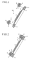
- the terminal 4 is press contacted with an electrode pad 3 of the display board or the circuit board P. Relation between each terminal 4 and each electrode pad 3 is shown in FIGS. 1 and 2.
- the probe supporting frame member 2 is provided with an attachment means such as attachment hole 5 for threadingly attaching the probe block B.
- the probe block B is threadingly attached to the probe supporting frame member 2 such that the terminals 4 are protruded towards an opening portion 16 of the frame member 2.
- FIGS. 7 to 10 One preferred example of the probe block supporting frame member 2 is shown in FIGS. 7 to 10 in which frame materials 12, 13, 14, 15 at four sides are cross assembled so that the probe block supporting frame member 2 may have an enlargable and reducible structure.
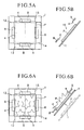
- FIGS. 4 to 6 Another preferred example of the probe block supporting frame member 2 is shown in FIGS. 4 to 6 in which the frame materials 12, 13, 14, 15 are separated and independent such that the probe block supporting frame member 2 may have an enlargable and reducible structure.
- a driving mechanism for enlarging and reducing the frame materials 12 to 15 comprises a motor 6, a ball screw 7 rotated by the motor 6 and a nut 8 threadingly engaged with the ball screw 7 and attached to the frame materials 12, 13, 14 15.
- the ball screw 7 is rotated by the motor 6, the nut 8 and the frame materials 12 to 15 are advanced or retracted depending on the direction of rotation.
- An amount of advancement or retraction is set by the number of rotation of the ball screw 7.
- an amount of enlargement and reduction of the opening portion 16 of the probe supporting frame member 2 is established.
- the board supporting frame member 1 shown in FIGS. 1 to 10 is supported by a driving mechanism which is advanced forward and retracted backward.
- the board supporting frame member 1 has a plurality of suction holes 11 which are open at a panel supporting surface and spacedly arranged in array in a longitudinal direction. Two to four sides of the display board or the circuit board P are suckingly retained by the suction holes 11 so that the board P is attachable and detachable.
- the frame materials 12 to 15 composing the probe supporting frame member 2 are retracted to enlarge the opening portion 16 defined by the frame materials 12 to 15. And the board supporting frame member 1 is relatively advanced. Due to advancement of the board supporting frame member 1, the display board or the circuit board P is protruded forward of a distal end of the terminal 4 of the probe block B through the enlarged opening portion 16, so that the display board or the circuit board P supported on the board supporting frame member 1 can be exchanged.
- the relative advancement of the board supporting frame member 1 is made by directly protruding the board supporting frame member 1 forward.
- the probe supporting frame member 2 is retracted backward to protrude the board supporting frame member 1 forward and in the remaining one of which both the probe supporting frame member 2 and the board supporting frame member 1 are moved to protrude the board supporting frame member 1 forward.
- the frame materials 12 to 15 at the four sides of the probe supporting frame member 2 are retracted on an open surface of the frame member from a reduction position (inspection position) by the driving mechanism, thereby enlarging the opening portion 16 so as to be larger than the board supporting frame member 1.
- the board supporting frame member 1 is advanced in a direction orthogonal to the open surface of the frame member from the rear standby position so that the display board or the circuit board P is protruded forward together with the board supporting frame member 1. That is to say, due to enlargement of the probe supporting frame member 2, the board supporting frame member 1 is retracted to a position where the terminal 4 does not interfere with the display board or the circuit board P. Otherwise, due to enlargement of the probe supporting frame member 2, the board supporting frame member 1 is retracted to a position where the terminal 4 does not interfere with the board P and the board supporting frame member 1. Then, the board supporting frame member 1 is advanced so that at least the board P is protruded to the front surface side of the terminal 4 through the enlarged opening portion 16.
- the sucking retaining of the board P is released to remove the board P from the board supporting frame member 1. Otherwise, the board P is removed from the board supporting frame member 1 without releasing the sucking retaining and then the sucking retaining is released.
- a new display board or a new circuit board P is placed on the board supporting frame member 1 and suckingly retained. Subsequently, the board supporting frame member 1 is retracted in a direction orthogonal to the open surface of the frame member 2 so as to form a rear standby position.
- the inspecting procedure will be described with reference to FIGS. 5 and 6.
- the frame materials 12 to 15 composing the probe supporting frame member 2 are, as shown in FIG. 5, advanced on the open surface of the frame member 2 to reduce the opening portion 16 of the probe supporting frame member 2 so that the terminal 4 of the probe block B is located above the corresponding electrode pad 3.
- the board supporting frame member 1 is moved forward in a direction orthogonal to the open surface of the frame member 2 from the rear standby position, so that the electrode pads 3 of the display board or the circuit board P are press contacted with the corresponding terminals 4 of the probe block B.
- the board supporting frame member 1 is moved forward in a direction orthogonal to the open surface of the frame member 2 from the rear standby position so that the electrode pads 3 of the display board or the circuit board P are press contacted with the corresponding terminals 4 of the probe block B. In that state, electric current is supplied to carry out an inspection. After the completion of inspection, the board supporting frame member 1 is retraced again to the rear standby position. Then, as described with reference to FIG. 4, the probe supporting frame member 2 is enlarged and the board supporting frame member 1 is advanced so that the board P can be exchanged.
- the exchange can be carried out within the occupation space at the time of inspection.
- the probe supporting frame member 2 comprises cross assembled four frame materials 12 to 15 composing the four sides.
- One pair of opposing frame materials 12, 14 are movably supported for advancement and retraction on the open surface of the frame member 2 in an X axis direction by the driving mechanism, and the other one pair of opposing frame materials 13, 15 are movably supported for advancement and retraction on the open surface of the frame member 2 in a Y axis direction by the driving mechanism.
- One end of the frame material 13 is cross assembled with an inner side of one end of the frame material 12, and one end of the frame material 14 is cross assembled with an inner side of the other end of the frame material 13.
- one end of the frame material 15 is cross assembled with an inner side of the other end of the frame material 14 and the other end of the frame material 12 is cross assembled with an inner side of the other end of the frame material 15.
- a rail 9 extending in a Y axis direction along inner sides of the frame material 12 and the frame material 14 is disposed between the mutually orthogonal frame materials 12 and 13 and between the mutually orthogonal frame materials 14 and 15.
- a slider 10 for slidingly engaged with the rail 9 is disposed on the frame material 13 and the frame material 15. Owing to this arrangement, when the slider 10 is slidingly moved along the rail 9, the frame material 13 and the frame material 15 are guided to move in the Y axis direction.
- a rail 9 extending in an X axis direction along inner sides of the frame material 13 and the frame material 15 is disposed between the frame materials 13 and 14 and between the frame materials 13 and 15.
- a slider 10 for slidingly engaged with the rail 9 is disposed on the frame material 14 and the frame material 12. Owing to this arrangement, when the slider 10 is slidingly moved along the rail 9, the frame material 14 and the frame material 12 are guided to move in the X axis direction.
- a driving mechanism for enlarging and reducing the frame materials 12 to 15 comprises a motor 6, a ball screw 7 rotated by the motor 6 and a nut 8 threadingly engaged with the ball screw 7 and attached to the frame materials 12 to 15.
- the ball screw 7 is rotated by the motor 6, the nut 8 and the frame materials 12 to 15 are advanced or retracted depending on the direction of rotation.
- An amount of advancement or retraction is set by the number of rotation of the ball screw 7.
- an amount of enlargement and reduction of the opening portion 16 of the probe supporting frame member 2 is established.
- the board supporting frame member 1 is supported by a driving mechanism which is advanced forward and retracted backward.
- the board supporting frame member 1 has a plurality of suction holes 11 which are open at a panel supporting surface and spacedly arranged in array in a longitudinal direction. Two to four sides of the display board or the circuit board P are suckingly retained by the suction holes 11 so that the board P is attachable and detachable.
- the frame materials 12 to 15 composing the probe supporting frame member 2 are retracted to enlarge the opening portion 16 defined by the frame materials 12 to 15. And the board supporting frame member 1 is relatively advanced. Due to advancement of the board supporting frame member 1, the display board or the circuit board P is protruded forward of a distal end of the terminal 4 of the probe block B through the enlarged opening portion 16, so that the display board or the circuit board P supported on the board supporting frame member 1 can be exchanged.
- the relative advancement of the board supporting frame member 1 is made by directly protruding the board supporting frame member 1 forward.
- the probe supporting frame member 2 is retracted backward to protrude the board supporting frame member 1 forward and in the remaining one of which both the probe supporting frame member 2 and the board supporting frame member 1 are moved to protrude the board supporting frame member 1 forward.
- the frame material 13 is also moved in the X axis direction through the cross assembly portion.
- the frame material 14 is also moved in the Y axis direction through the cross assembly portion.
- the frame material 15 is also moved in the X axis direction through the cross assembly portion.
- the frame material 12 is also moved in the Y axis direction through the cross assembly portion.
- the board supporting frame member 1 After the probe supporting frame member 2 is reduced to the board inspection position, as shown in FIGS. 2 and 6, the board supporting frame member 1 is advanced in a direction orthogonal to the open surface of the frame member 2 from the rear standby position, the electrode pads 3 of the board P are press contacted with the corresponding terminals 4 and inspection is carried out in that state.
- the frame material 15 When the frame material 15 is retracted on the open surface in the Y axis direction by the driving mechanism, the frame material 12 is also moved in the Y axis direction through the cross assembly portion. Thus, due to the movement mentioned above, the opening portion 16 of the probe supporting frame member 2 is enlarged to form a board exchange position.
- the board supporting frame member 1 is advanced in a direction orthogonal to the opening surface of the frame member 2 from the board standby position, so that at least the board P is protruded through the enlarged opening portion 16 to a position where it does not interfere with the distal end of the terminal 4. And the board is exchanged to new one in that state.
- the display board or the circuit board can be exchanged generally in an occupation space at the time of inspection, and no side space for exchange, which is required in the prior art, is needed, and an apparatus for inspecting a display board or a circuit board can greatly be miniaturized.
Landscapes
- Engineering & Computer Science (AREA)
- Physics & Mathematics (AREA)
- Computer Hardware Design (AREA)
- General Physics & Mathematics (AREA)
- Theoretical Computer Science (AREA)
- Measuring Leads Or Probes (AREA)
- Tests Of Electronic Circuits (AREA)
- Devices For Indicating Variable Information By Combining Individual Elements (AREA)
- Liquid Crystal (AREA)
- Testing Of Short-Circuits, Discontinuities, Leakage, Or Incorrect Line Connections (AREA)
Applications Claiming Priority (2)
| Application Number | Priority Date | Filing Date | Title |
|---|---|---|---|
| JP2000315081 | 2000-10-16 | ||
| JP2000315081A JP3457938B2 (ja) | 2000-10-16 | 2000-10-16 | 表示基板又は回路基板の検査装置における表示基板又は回路基板の交換方法 |
Publications (2)
| Publication Number | Publication Date |
|---|---|
| EP1199571A2 true EP1199571A2 (de) | 2002-04-24 |
| EP1199571A3 EP1199571A3 (de) | 2003-08-13 |
Family
ID=18794236
Family Applications (1)
| Application Number | Title | Priority Date | Filing Date |
|---|---|---|---|
| EP01308142A Withdrawn EP1199571A3 (de) | 2000-10-16 | 2001-09-25 | Inspektionsvorrichtung für Anzeigekarten oder Leiterplatten |
Country Status (6)
| Country | Link |
|---|---|
| US (1) | US6590406B2 (de) |
| EP (1) | EP1199571A3 (de) |
| JP (1) | JP3457938B2 (de) |
| KR (1) | KR100767298B1 (de) |
| CN (1) | CN1349100A (de) |
| TW (1) | TW522241B (de) |
Families Citing this family (8)
| Publication number | Priority date | Publication date | Assignee | Title |
|---|---|---|---|---|
| CN100504417C (zh) * | 2003-08-05 | 2009-06-24 | 奇美电子股份有限公司 | 液晶显示面板的多功能检测机台及其检测方法 |
| JP2006138634A (ja) * | 2004-10-15 | 2006-06-01 | Micronics Japan Co Ltd | 表示用パネルの検査装置に用いられる電気的接続装置 |
| TWI281026B (en) * | 2004-12-30 | 2007-05-11 | De & T Co Ltd | Needle assembly of probe unit for testing flat display panel |
| JP5424015B2 (ja) * | 2008-11-18 | 2014-02-26 | 日本電産リード株式会社 | 基板保持装置及び基板検査装置 |
| JP6084426B2 (ja) * | 2012-10-15 | 2017-02-22 | 株式会社日本マイクロニクス | 検査装置 |
| JP6422376B2 (ja) * | 2015-03-06 | 2018-11-14 | 三菱電機株式会社 | 半導体装置検査用治具 |
| CN105430923B (zh) * | 2015-12-24 | 2018-05-18 | 竞陆电子(昆山)有限公司 | 基板外观/色泽检查设备的上板区域改进结构 |
| CN214025309U (zh) * | 2020-10-30 | 2021-08-24 | 京东方科技集团股份有限公司 | 测试夹具 |
Family Cites Families (11)
| Publication number | Priority date | Publication date | Assignee | Title |
|---|---|---|---|---|
| JPS5391376A (en) * | 1977-01-24 | 1978-08-11 | Hirohide Yano | Device for inspecting printed board |
| US4841231A (en) * | 1987-10-30 | 1989-06-20 | Unisys Corporation | Test probe accessibility method and tool |
| JPH0799379B2 (ja) * | 1987-11-30 | 1995-10-25 | 東京エレクトロン九州株式会社 | プローブ装置 |
| JPH04330753A (ja) * | 1991-01-16 | 1992-11-18 | Tokyo Electron Ltd | 半導体検査装置及び半導体検査方法 |
| DE69109869T2 (de) * | 1991-12-06 | 1995-09-21 | Sigmatech Co Ltd | Apparat zur Inspektion der inneren Schaltung eines Halbleiters. |
| JPH0878122A (ja) * | 1994-09-02 | 1996-03-22 | Hitachi Ltd | 接続装置 |
| JPH08254677A (ja) * | 1994-10-14 | 1996-10-01 | Hitachi Electron Eng Co Ltd | 液晶パネルの点灯試験用コンタクト装置 |
| JPH10132706A (ja) * | 1996-11-01 | 1998-05-22 | Micronics Japan Co Ltd | 液晶表示パネルの検査装置 |
| JPH1140302A (ja) * | 1997-07-25 | 1999-02-12 | Nec Corp | フリーサイズlsiピン変換治具 |
| US6420884B1 (en) * | 1999-01-29 | 2002-07-16 | Advantest Corp. | Contact structure formed by photolithography process |
| JP3350899B2 (ja) * | 1999-08-31 | 2002-11-25 | 株式会社双晶テック | プローブブロックの支持枠体 |
-
2000
- 2000-10-16 JP JP2000315081A patent/JP3457938B2/ja not_active Expired - Lifetime
-
2001
- 2001-09-25 EP EP01308142A patent/EP1199571A3/de not_active Withdrawn
- 2001-09-25 KR KR1020010059204A patent/KR100767298B1/ko not_active Expired - Lifetime
- 2001-10-12 US US09/974,895 patent/US6590406B2/en not_active Expired - Fee Related
- 2001-10-16 TW TW090125571A patent/TW522241B/zh not_active IP Right Cessation
- 2001-10-16 CN CN01135783A patent/CN1349100A/zh active Pending
Also Published As
| Publication number | Publication date |
|---|---|
| TW522241B (en) | 2003-03-01 |
| JP3457938B2 (ja) | 2003-10-20 |
| KR100767298B1 (ko) | 2007-10-16 |
| US20020043982A1 (en) | 2002-04-18 |
| KR20020030253A (ko) | 2002-04-24 |
| CN1349100A (zh) | 2002-05-15 |
| JP2002123189A (ja) | 2002-04-26 |
| EP1199571A3 (de) | 2003-08-13 |
| US6590406B2 (en) | 2003-07-08 |
Similar Documents
| Publication | Publication Date | Title |
|---|---|---|
| US6450469B1 (en) | Flat panel display or probe block support framework | |
| KR102004441B1 (ko) | 핀 보드 조립체 | |
| KR100786631B1 (ko) | 디스플레이 패널 또는 프로브 블록의 지지틀 | |
| KR100940505B1 (ko) | 디스플레이 패널 검사를 위한 프로브 유닛 | |
| EP1199571A2 (de) | Inpektionsvorrichtung für Anzeigekarten oder Leiterplatten | |
| US7355418B2 (en) | Configurable prober for TFT LCD array test | |
| US7471095B2 (en) | Electrical connecting apparatus and method for use thereof | |
| JPH0738231A (ja) | クリーム半田用メタルマスクおよび枠への取付方法 | |
| JPH1154574A (ja) | クリーニング方法及びプローブ装置 | |
| JP3538696B2 (ja) | プローブ装置の組立方法 | |
| JP4196065B2 (ja) | ディスプレイパネルの点灯検査装置 | |
| JP3960585B2 (ja) | フラックス転写機構 | |
| CN113541790B (zh) | 光通信器件的测试系统及其操作方法 | |
| CN216386817U (zh) | 电路板自动测试设备 | |
| KR102694889B1 (ko) | 디스플레이 패널 검사용 컨택유닛 | |
| CN219498462U (zh) | 一种用于连接器扣合的辅助工装 | |
| CN218217349U (zh) | Sim卡安装装置及终端 | |
| JP4196082B2 (ja) | ディスプレイパネルの点灯検査装置 | |
| JP2003028927A (ja) | ソフト書込・検査装置 | |
| JPH0354676A (ja) | マーキング装置における版監視方法及び装置 | |
| JP2000065861A (ja) | プローブ装置の微調整機構 | |
| JP2003139654A (ja) | フラットパネルディスプレイの支持枠体 | |
| JP3324400B2 (ja) | 基板移送装置 | |
| JPH1065370A (ja) | 基板収納装置 | |
| JP2002036494A (ja) | スクリーン版クリーニングユニット |
Legal Events
| Date | Code | Title | Description |
|---|---|---|---|
| PUAI | Public reference made under article 153(3) epc to a published international application that has entered the european phase |
Free format text: ORIGINAL CODE: 0009012 |
|
| AK | Designated contracting states |
Kind code of ref document: A2 Designated state(s): AT BE CH CY DE DK ES FI FR GB GR IE IT LI LU MC NL PT SE TR |
|
| AX | Request for extension of the european patent |
Free format text: AL;LT;LV;MK;RO;SI |
|
| PUAL | Search report despatched |
Free format text: ORIGINAL CODE: 0009013 |
|
| AK | Designated contracting states |
Designated state(s): AT BE CH CY DE DK ES FI FR GB GR IE IT LI LU MC NL PT SE TR |
|
| AX | Request for extension of the european patent |
Extension state: AL LT LV MK RO SI |
|
| AKX | Designation fees paid | ||
| REG | Reference to a national code |
Ref country code: DE Ref legal event code: 8566 |
|
| STAA | Information on the status of an ep patent application or granted ep patent |
Free format text: STATUS: THE APPLICATION IS DEEMED TO BE WITHDRAWN |
|
| 18D | Application deemed to be withdrawn |
Effective date: 20040401 |