EP1206036A2 - Akustisches Oberflächenwellenfilter und akustische Oberflächenwellenvorrichtung - Google Patents
Akustisches Oberflächenwellenfilter und akustische Oberflächenwellenvorrichtung Download PDFInfo
- Publication number
- EP1206036A2 EP1206036A2 EP01126680A EP01126680A EP1206036A2 EP 1206036 A2 EP1206036 A2 EP 1206036A2 EP 01126680 A EP01126680 A EP 01126680A EP 01126680 A EP01126680 A EP 01126680A EP 1206036 A2 EP1206036 A2 EP 1206036A2
- Authority
- EP
- European Patent Office
- Prior art keywords
- comb electrode
- package
- electrode patterns
- chip substrate
- saw filter
- Prior art date
- Legal status (The legal status is an assumption and is not a legal conclusion. Google has not performed a legal analysis and makes no representation as to the accuracy of the status listed.)
- Withdrawn
Links
Images



Classifications
-
- H—ELECTRICITY
- H03—ELECTRONIC CIRCUITRY
- H03H—IMPEDANCE NETWORKS, e.g. RESONANT CIRCUITS; RESONATORS
- H03H9/00—Networks comprising electromechanical or electro-acoustic elements; Electromechanical resonators
- H03H9/02—Details
- H03H9/02535—Details of surface acoustic wave devices
- H03H9/02818—Means for compensation or elimination of undesirable effects
- H03H9/02921—Measures for preventing electric discharge due to pyroelectricity
-
- H—ELECTRICITY
- H03—ELECTRONIC CIRCUITRY
- H03H—IMPEDANCE NETWORKS, e.g. RESONANT CIRCUITS; RESONATORS
- H03H9/00—Networks comprising electromechanical or electro-acoustic elements; Electromechanical resonators
- H03H9/02—Details
- H03H9/05—Holders or supports
- H03H9/10—Mounting in enclosures
- H03H9/1064—Mounting in enclosures for surface acoustic wave [SAW] devices
- H03H9/1071—Mounting in enclosures for surface acoustic wave [SAW] devices the enclosure being defined by a frame built on a substrate and a cap, the frame having no mechanical contact with the SAW device
Definitions
- the present invention relates to a surface acoustic wave filter and surface acoustic wave filter apparatus used in an optical communication device and mobile radio communication device.
- a surface acoustic wave filter (to be referred to as SAW (Surface Acoustic Wave) filter hereinafter) has features such as compactness, high stability, high precision, high reliability, and no need for adjustment, and is widely used as a functional element for controlling an RF signal in an optical communication device and mobile communication device.
- SAW Surface Acoustic Wave
- the SAW filter is used as a functional element such as a frequency selection element, filter element, resonator, and delay element.
- the SAW filter controls an electrical RF signal through a surface acoustic wave propagating on the surface of the base material.
- a piezoelectric material such as rock crystal, LBO, lithium tantalate (LiTaO 3 ), or lithium niobate (LiNbO 3 ) is generally used.
- a base material made of a piezoelectric material is called a chip substrate.
- a plurality of come electrode patterns are formed on the chip substrate by using, e.g., the thin film formation technique and photolithography technique.
- the SAW filter In the SAW filter, a pair of comb electrode patterns, or several pairs of comb electrode patterns arranged in the propagating direction of the surface acoustic wave are formed.
- the SAW filter can select a frequency which depends on the line width of the comb electrode patterns by converting an electrical RF signal into a surface acoustic wave and vice versa on a surface wave propagation path serving as a range where the comb electrode patterns are formed.
- the SAW filter is generally used as it is accommodated in a package.
- a SAW filter accommodated in a package is called a SAW filter apparatus.
- the comb electrode patterns are connected, through bonding wires or the like, to an input signal electrode terminal, output signal electrode terminal, and ground terminals formed on a package which is to accommodate the SAW filter.
- the piezoelectric material has pyroelectric properties.
- polarization may occur in the piezoelectric material to generate charges on the surface of the chip substrate.
- charges When charges are generated on the surface of the chip substrate, they produce an electric field on the comb electrode patterns.
- discharge occurs between the comb electrode patterns. In the worst case, pattern destruction is caused by discharge.
- a package made of a ceramic material is used as the package for accommodating the SAW filter, and a metal film is formed on the bottom surface of the interior of the package by plating or vapor deposition. More specifically, a ceramic package, in which a metal film comes into contact with the lower surface of the chip substrate of the SAW filter when the SAW filter is accommodated in it, is used. Then, the ground electrode of the SAW filter and the metal film are connected to each other. When this package is used, even if polarization occurs to generate charges, the generated charges are released to the metal film, and destruction of the comb electrode patterns is prevented.
- a plastic package is sometimes used in order to reduce the manufacturing cost of the SAW filter. It is, however, difficult to form a metal film on the plastic package by plating or vapor deposition. In other words, it is difficult to provide a package with a means for releasing charges which are generated when polarization occurs. Accordingly, a SAW filter cannot but be packaged with no metal film being present between the plastic package and SAW filter. As a result, to be able to use a plastic package, it is important that the chip substrate itself of the SAW filter have a structure with which polarization does not occur or which releases charges generated when polarization occurs.
- the present invention has been made in consideration of the above situation in the prior art, and has as its object to provide a SAW filter with a structure that can prevent the comb electrode patterns from being destroyed by charges generated when polarization occurs, and a SAW filter apparatus with a structure that can prevent the comb electrode patterns from being destroyed by charges even if no countermeasure is taken on the package side.
- a surface acoustic wave filter in which a plurality of pairs of comb electrode patterns are formed on an upper surface of a chip substrate made of a piezoelectric material, comprising a high-resistance pattern formed to surround a peripheral portion of the chip substrate on an upper surface side, and a plurality of patterns formed to connect the high-resistance pattern to the respective comb electrode patterns.
- a surface acoustic wave filter in which a plurality of pairs of comb electrode patterns are formed on an upper surface of a chip substrate made of a piezoelectric material, comprising a first pattern formed on the upper surface of the chip substrate so as to extend from part of at least one member of each of the pairs of comb electrode patterns, a second pattern formed on the upper surface of the chip substrate so as to oppose the first pattern at a predetermined gap, and a dummy electrode pattern formed on the upper surface of the chip substrate so as to be adjacent to the second pattern and connected thereto.
- a surface acoustic wave filter in which a plurality of pairs of comb electrode patterns are formed on an upper surface of a chip substrate made of a piezoelectric material, wherein opposing portions of two comb electrode patterns that form a pair are not sharp.
- a surface acoustic wave filter apparatus is obtained by accommodating either one of the surface acoustic wave filters according to the first to third aspects in a plastic package.
- a metal plate-like-portion is formed at a center of the package that accommodates the surface acoustic wave filter, and a lower surface of the chip substrate which constitutes the surface acoustic wave filter is fixed to the package with a conductive adhesive.
- the SAW filter has the high-resistance pattern to surround the peripheral portion of the chip substrate on the upper surface side, and the patterns to connect the respective comb electrode patterns to the high-resistance pattern.
- the comb electrode patterns are set at the same potential, and accordingly discharge between the comb electrode patterns can be prevented, so destruction of the comb electrode patterns can be prevented.
- the first pattern formed by extending part of the comb electrode pattern, the second pattern formed to oppose the first pattern at the predetermined gap, and the dummy electrode pattern to be connected to the second pattern are formed on the upper surface of the chip substrate, even if polarization occurs in the chip substrate to generate charges, thus causing discharge, this discharge occurs in the gap, so discharge between the comb electrode patterns can be prevented.
- Fig. 1A is a plan view of a SAW filter according to the first embodiment of the present invention
- Fig. 1B is a sectional view taken along the line IB - IB of Fig. 1A.
- comb electrode patterns 11, 12, 13, and 14 are formed of Al (aluminum) thin films, Al alloy thin films, or the like on a chip substrate 1 made of a piezoelectric material such as lithium tantalate (LiTaO 3 ) or lithium niobate (LiNbO 3 ).
- the comb electrode patterns 11, 12, 13, and 14 are connected through bonding wires (not shown) to an input signal electrode terminal, output signal electrode terminal, and ground electrode terminals formed on a package which accommodates the SAW filter.
- the comb electrode pattern 13 serves as an input signal electrode and is connected to the input signal electrode terminal
- the comb electrode pattern 12 serves as an output signal electrode and is connected to the output signal electrode terminal.
- the comb electrode patterns 11 and 14 serve as ground electrodes and are connected to the ground electrode terminal.
- a coating film made of a conductive material 3 such as Al covers the entire area of the lower surface of the chip substrate 1, and the comb electrode patterns serving as the ground electrodes and the metal film on the lower surface of the chip substrate 1 are connected to each other through the conductive material 3.
- Fig. 1B shows a case wherein the comb electrode pattern 14 and the metal film are connected to each other through the conductive material 3.
- the structure shown in Figs. 1A and 1B is particularly effective when a plastic package is used as the package for accommodating the SAW filter. If the SAW filter with the structure shown in Figs. 1A and 1B is accommodated in a ceramic package, destruction of the comb electrode patterns 11, 12, 13, and 14 can be prevented without taking a countermeasure such as forming a metal film on the bottom surface of the ceramic package.
- Fig. 2A is a plan view showing a SAW filter according to the second embodiment of the present invention
- Fig. 2B is a sectional view taken along the line IIB - IIB of Fig. 2A.
- comb electrode patterns 11, 12, 13, and 14 are formed on a chip substrate 1 made of a piezoelectric material, and the peripheral portion of the chip substrate 1 on the upper surface side is covered with a film made of a conductive material 3 such as a metal.
- the film made of the conductive material 3 does not cover a surface wave propagation path of the SAW filter.
- the peripheral portion of the chip substrate 1 on the upper surface side is formed with a film made of the conductive material 3, even if charges are generated by polarization, they are released to the film made of the conductive material 3, and are not concentrated at the portions of the comb electrode patterns 11, 12, 13, and 14. In other words, undesirable charge concentration at the specific portions of the comb electrode patterns 11, 12, 13, and 14 can be avoided, and discharge between the comb electrode patterns 11, 12, 13, and 14 is prevented. Since charge concentration at specific portions can be avoided, the film made of the conductive material 3 practically serves to neutralize the charges in the chip substrate 1.
- the structure shown in Figs. 2A and 2B is also particularly effective when a plastic package is used as the package for accommodating the SAW filter. If the SAW filter with the structure shown in Figs. 2A and 2B is accommodated in a ceramic package, destruction of the comb electrode patterns 11, 12, 13, and 14 can be prevented without taking a countermeasure such as forming a metal film on the bottom surface of the ceramic package.
- Fig. 3A is a plan view showing a SAW filter according to the third embodiment of the present invention
- Fig. 3B is a sectional view taken along the line B - B of Fig. 3A.
- comb electrode patterns 11, 12, 13, and 14 are formed on a chip substrate 1 made of a piezoelectric material, and are connected to each other through patterns 41 exhibiting a high resistance and made of Ti or the like.
- a pattern 4 exhibiting a high resistance is formed on the peripheral portion of the chip substrate 1 on the upper surface side.
- a material such as Ti (titanium) or Si (silicon) with a high resistivity on the order of M ⁇ or more is used as the material of the high-resistance pattern 4.
- SiO 2 may be used as the material of the high-resistance pattern 4.
- the material of the high-resistance pattern 4 is the same as that of the patterns 41.
- the high-resistance pattern 4 does not cover the surface wave propagation path portion of the SAW filter.
- Each of the patterns 41 has such a thickness that does not adversely affect the surface acoustic wave.
- the high-resistance patterns 4 and 41 connect the comb electrode patterns 11, 12, 13, and 14 to each other, they do not adversely influence the performance of the comb electrode patterns 11, 12, 13, and 14.
- the structure shown in Figs. 3A and 3B is also particularly effective when a plastic package is used as the package for accommodating the SAW filter. If the SAW filter with the structure shown in Figs. 3A and 3B is accommodated in a ceramic package, destruction of the comb electrode patterns 11, 12, 13, and 14 can be prevented without taking a countermeasure such as forming a metal film on the bottom surface of the ceramic package.
- Fig. 4 is a plan view showing part of a SAW filter according to the fourth embodiment of the present invention.
- comb electrode patterns 11, 12, 13, and 14 are formed on a chip substrate 1 made of a piezoelectric material.
- the comb electrode patterns 12 and 14 partly extend on the upper surface of the chip substrate 1, thus forming patterns 51 serving as the first pattern.
- Fig. 4 shows one pair.
- a pattern 52 with the same line width as that of each pattern 51 and serving as the second pattern is formed to oppose the pattern 51 at a gap 53.
- the width of the gap 53 (the length between the patterns 51 and 52) is smaller than that of the gap between the comb electrode pattern 11 or 13 and the comb electrode pattern 12 or 14.
- the line width of each of the patterns 51 and 52 is smaller than the pattern width of each of the comb electrode patterns 11, 12, 13, and 14.
- the structure shown in Fig. 4 is also particularly effective when a plastic package is used as the package for accommodating the SAW filter. If the SAW filter with the structure shown in Fig. 4 is accommodated in a ceramic package, destruction of the comb electrode patterns 11, 12, 13, and 14 can be prevented without taking a countermeasure such as forming a metal film on the bottom surface of the ceramic package.
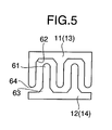
- Fig. 5 is a plan view showing part of a SAW filter according to the fifth embodiment of the present invention.
- comb electrode patterns 11, 12, 13, and 14 are formed on a chip substrate 1 made of a piezoelectric material. As shown in Fig. 5, the distal ends and corners of the respective comb electrode patterns 11, 12, 13, and 14 are rounded. More specifically, of the respective comb electrode patterns 11, 12, 13, and 14, portions 61, 62, 63, and 64 each opposing a comb electrode pattern with which it makes a pair are rounded.
- the structure shown in Fig. 5 is also particularly effective when a plastic package is used as the package for accommodating the SAW filter. If the SAW filter with the structure shown in Fig. 5 is accommodated in a ceramic package, destruction of the comb electrode patterns 11, 12, 13, and 14 can be prevented without taking a countermeasure such as forming a metal film on the bottom surface of the ceramic package.
- any one of the structures employed in the first to fifth embodiments described above can prevent destruction of the comb electrode patterns 11, 12, 13, and 14 caused by the pyroelectric effect of the chip substrate 1 without taking any countermeasure on the package side.
- two, three, or more structures may be combined. When a plurality of structures are combined, destruction of the comb electrode patterns 11, 12, 13, and 14 caused by the pyroelectric effect can be prevented more reliably.
- a charge neutralizing means practically serving to neutralize or diffuse charges is realized.
- a means for rendering the potential common is realized as well as the charge neutralizing means, and in the fourth and fifth embodiments, a charge escape means is realized as well as the charge neutralizing means.
- a means for rendering the potential common is realized.
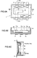
- Fig. 6A is a plan view showing an arrangement of a package suitable for accommodating a SAW filter
- Fig. 6B is a sectional view taken along the line VIB - VIB of Fig. 6A
- Fig. 6C is a sectional view taken along the line VIC - VIC of Fig. 6A.
- a package 7 has a rectangular planar shape, and a wall-like peripheral portion.
- a rectangular groove 78 where a SAW filter is to be set is formed at the center of the package 7.
- a plurality of pads 71a, 72a, 73a, 75a, and 76a are formed on a shelf-like portion 79 between a wall-like portion (wall) 77 formed at the peripheral portion and the groove 78 at the center.
- Metal terminals 71, 72, 73, 74, 75, and 76 extend from the inside of the package 7 to the outside.
- the terminal 74 is used as a ground terminal (GND terminal).
- the respective pads 71a, 72a, 73a, 75a, and 76a are integrally formed with the corresponding terminals 71, 72, 73, 75, and 76.
- the GND terminal 74 extends to the inside of the package 7, and has a portion extending horizontally (horizontal extending portion) from the extending portion (vertical extending portion).
- the vertical and horizontal extending portions of the GND terminal 74 form a metal plate-like portion 80 exposed to the groove 78 in the package 7.
- a plurality of GND terminals may be formed. For example, when two GND terminals are formed, they are integrated with the plate-like portion 80 exposed to the groove 78. In this case, since the plate-like portion 80 exposed in the groove 78 is supported at two portions, its posture is stabilized.
- Figs. 7A and 7B are plan and sectional views, respectively, showing a state wherein a SAW filter 100 is accommodated in the package 7 shown in Figs. 6A to 6C.
- the SAW filter 100 is set in the groove 78 of the package 7 such that the lower surface of the chip substrate comes into contact with the plate-like portion 80.
- the comb electrode patterns 11, 12, 13, and 14 and the predetermined pads 71a, 72a, 75a, and 76a are connected to each other through bonding wires 71b, 72b, 75b, and 76b.
- the upper surface of the package 7 is closed with a plastic member of the like.
- the package 7 shown in Figs. 6A to 6C has the metal plate-like portion 80.
- the plate-like portion 80 is integrated with the GND terminal 74.
- the metal plate comes into contact with the lower surface of the chip substrate. It is thus expected that charges generated by polarization will be neutralized without concentrating at the upper surface of the chip substrate of the SAW filter 100.
- undesirable charge concentration at the specific portions of the comb electrode patterns 11, 12, 13, and 14 can be avoided.
- discharge between the comb electrode patterns 11, 12, 13, and 14 is prevented.
- the GND terminal 74 is electrically connected to the outside through a portion outside the package 7 (e.g., on the printed wiring board), the GND terminal 74 and a comb electrode pattern serving as a ground electrode can be connected to each other.
- a state wherein the GND terminal 74 and the comb electrode pattern are connected to each other is similar to the state of the first embodiment shown in Figs. 1A and 1B. In this state, charges generated by polarization based on the pyroelectric effect can be expected to neutralize, and can be released to the metal plate located on the lower surface of the chip substrate through the comb electrode pattern. Therefore, undesirable charge concentration at the specific portions of the comb electrode patterns 11, 12, 13, and 14 can be avoided more effectively.
- the package 7 of this embodiment even if no countermeasure against the charges generated by polarization is taken on the side of the SAW filter itself, destruction of the comb electrode patterns 11, 12, 13, and 14 can be prevented.
- a SAW filter that has undergone a countermeasure as shown in the above first to fifth embodiments is accommodated in the package 7 shown in Figs. 6A to 6C, destruction of the comb electrode patterns 11, 12, 13, and 14 can be prevented more reliably.
- the SAW filter apparatus in which a SAW filter according to the first to fifth embodiments is accommodated in the package 7 shown in Figs. 6A to 6C is more resistant against destruction of the comb electrode patterns 11, 12, 13, and 14.
- the metal plate-like portion 80 is integrated with the GND terminal 74.
- the metal plate-like portion 80 is formed by only forming an L-shaped metal plate as the GND terminal 74.
- the process for forming the package 7 does not become complicated.
- the structure shown in Figs. 6A to 6C can thus be employed for the ceramic package. In this case, the manufacturing process can be simplified when compared to a case wherein a metal film is formed on the bottom surface in the package by plating or vapor deposition.
- the SAW filter 100 when the SAW filter 100 is to be accommodated in the package 7 shown in Figs. 6A to 6C, it may be fixed to the package 7 with a conductive adhesive 81, as shown in Fig. 7B. As shown in Fig. 7B, the metal plate-like portion 80 is located between the SAW filter 100 and package 7. When fixing the SAW filter 100 to the package 7 with the conductive adhesive 81, connection between the SAW filter 100 and plate-like portion 80 becomes firm. Therefore, electrical connection between the SAW filter 100 and the metal plate-like portion 80 can become more reliable.
- the structure of the chip substrate 1 itself of the SAW filter can neutralize or release charges generated by polarization.
- this SAW filter is accommodated in a plastic package, even if a sharp temperature change occurs in the surrounding environment, destruction of the comb electrode patterns 11, 12, 13, and 14 can be prevented.
- a SAW filter apparatus in which a SAW filter with a structure according to the first to fifth embodiments is accommodated in a plastic package, even if a sharp temperature change occurs in the surrounding environment, destruction of the comb electrode patterns 11, 12, 13, and 14 can be prevented.
- the chip substrate 1 with the structure shown in the first to fifth embodiments can be accommodated in a ceramic package.
- a metal plate with which the lower surface of the chip substrate comes into contact when a SAW filter is to be accommodated can be formed without using plating or vapor deposition.
Landscapes
- Physics & Mathematics (AREA)
- Acoustics & Sound (AREA)
- Surface Acoustic Wave Elements And Circuit Networks Thereof (AREA)
Applications Claiming Priority (2)
| Application Number | Priority Date | Filing Date | Title |
|---|---|---|---|
| JP2000342687A JP2002152001A (ja) | 2000-11-09 | 2000-11-09 | 弾性表面波フィルタおよび弾性表面波フィルタ装置 |
| JP2000342687 | 2000-11-09 |
Publications (2)
| Publication Number | Publication Date |
|---|---|
| EP1206036A2 true EP1206036A2 (de) | 2002-05-15 |
| EP1206036A3 EP1206036A3 (de) | 2008-10-22 |
Family
ID=18817187
Family Applications (1)
| Application Number | Title | Priority Date | Filing Date |
|---|---|---|---|
| EP01126680A Withdrawn EP1206036A3 (de) | 2000-11-09 | 2001-11-08 | Akustisches Oberflächenwellenfilter und akustische Oberflächenwellenvorrichtung |
Country Status (3)
| Country | Link |
|---|---|
| US (1) | US6750592B2 (de) |
| EP (1) | EP1206036A3 (de) |
| JP (1) | JP2002152001A (de) |
Families Citing this family (13)
| Publication number | Priority date | Publication date | Assignee | Title |
|---|---|---|---|---|
| EP1381156A4 (de) * | 2001-04-19 | 2004-09-08 | Matsushita Electric Industrial Co Ltd | Oberflächenwellenbauelement und verfahren zu seiner herstellung und elektronisches bauelement damit |
| JP2004297619A (ja) | 2003-03-27 | 2004-10-21 | Kyocera Corp | 弾性表面波装置 |
| JP2004364041A (ja) * | 2003-06-05 | 2004-12-24 | Fujitsu Media Device Kk | 弾性表面波デバイス及びその製造方法 |
| JP4419732B2 (ja) * | 2003-09-02 | 2010-02-24 | 株式会社村田製作所 | 弾性表面波装置およびその製造方法 |
| JP4610244B2 (ja) * | 2004-06-28 | 2011-01-12 | 京セラ株式会社 | 弾性表面波装置の製造方法 |
| JP4514572B2 (ja) * | 2004-09-15 | 2010-07-28 | 京セラ株式会社 | 弾性表面波装置および通信装置 |
| US7389570B2 (en) * | 2004-06-28 | 2008-06-24 | Kyocera Corporation | Surface acoustic wave device manufacturing method, surface acoustic wave device, and communications equipment |
| JP4514571B2 (ja) * | 2004-09-15 | 2010-07-28 | 京セラ株式会社 | 弾性表面波装置およびその製造方法ならびに通信装置 |
| WO2007125724A1 (ja) * | 2006-04-28 | 2007-11-08 | Murata Manufacturing Co., Ltd. | 電子部品及びその製造方法 |
| US9225311B2 (en) | 2012-02-21 | 2015-12-29 | International Business Machines Corporation | Method of manufacturing switchable filters |
| DE102013105999A1 (de) * | 2013-06-10 | 2014-12-24 | Epcos Ag | Mobilfunkgerät mit gemeinsam genutztem Filter, Verfahren zum Betrieb des Mobilfunkgeräts und Verwendung eines Filters |
| JP6115408B2 (ja) * | 2013-08-29 | 2017-04-19 | 三菱電機株式会社 | 半導体装置 |
| DE102016118124B4 (de) * | 2016-09-26 | 2023-11-30 | Snaptrack, Inc. | Elektroakustischer Wandler mit verbesserter ESD Festigkeit |
Family Cites Families (22)
| Publication number | Priority date | Publication date | Assignee | Title |
|---|---|---|---|---|
| JPS56149110A (en) * | 1980-04-22 | 1981-11-18 | Fujitsu Ltd | Elastic surface wave device |
| JPS60124109A (ja) | 1983-12-09 | 1985-07-03 | Clarion Co Ltd | 表面弾性波素子 |
| JPH0278314A (ja) * | 1988-09-14 | 1990-03-19 | Hitachi Ltd | 弾性表面波装置 |
| JPH02177609A (ja) * | 1988-12-27 | 1990-07-10 | Nec Corp | 表面弾性波デバイス |
| US5837332A (en) * | 1989-11-19 | 1998-11-17 | Nihon Victor Kabushiki-Kaisha | Method and apparatus for preparing crystal thin films by using a surface acoustic wave |
| JPH03284006A (ja) * | 1990-03-30 | 1991-12-13 | Fujitsu Ltd | 弾性表面波デバイス |
| JP2673993B2 (ja) * | 1990-07-02 | 1997-11-05 | 日本無線株式会社 | 表面弾性波装置 |
| JP3301168B2 (ja) | 1993-07-27 | 2002-07-15 | 富士通株式会社 | 表面弾性波フィルタとその製造方法 |
| JP3106387B2 (ja) * | 1995-04-04 | 2000-11-06 | 株式会社村田製作所 | 弾性表面波装置 |
| JPH0983288A (ja) * | 1995-09-19 | 1997-03-28 | Japan Radio Co Ltd | 表面弾性波素子 |
| JPH09172349A (ja) | 1995-12-20 | 1997-06-30 | Matsushita Electric Ind Co Ltd | 表面弾性波素子およびその製造方法 |
| JPH09186550A (ja) * | 1995-12-27 | 1997-07-15 | Sanyo Electric Co Ltd | チップ設置台及びこれを用いたパッケージ及び弾性波フィルタ装置 |
| KR20000067918A (ko) * | 1996-07-19 | 2000-11-25 | 야마모토 카즈모토 | 탄성 표면파 기능 소자 |
| JPH10190394A (ja) * | 1996-12-25 | 1998-07-21 | Murata Mfg Co Ltd | 弾性表面波共振子フィルタ |
| JPH1188107A (ja) | 1997-09-02 | 1999-03-30 | Nec Corp | 弾性表面波デバイス |
| JPH11225038A (ja) * | 1998-02-06 | 1999-08-17 | Murata Mfg Co Ltd | 弾性表面波装置 |
| JP3280617B2 (ja) * | 1998-02-27 | 2002-05-13 | 東洋通信機株式会社 | 広帯域表面波フィルタ |
| JP2000068778A (ja) * | 1998-08-21 | 2000-03-03 | Murata Mfg Co Ltd | 表面波共振子、表面波フィルタ、共用器、通信機装置及び表面波デバイス、ならびに表面波共振子の製造方法 |
| JP3353742B2 (ja) * | 1999-05-07 | 2002-12-03 | 株式会社村田製作所 | 表面波共振子、表面波装置、通信機装置 |
| US6426583B1 (en) * | 1999-06-14 | 2002-07-30 | Matsushita Electric Industrial Co., Ltd. | Surface acoustic wave element, method for producing the same and surface acoustic wave device using the same |
| JP2001136048A (ja) * | 1999-11-09 | 2001-05-18 | Nec Corp | 弾性表面波フィルタ |
| JP3412611B2 (ja) * | 2000-09-25 | 2003-06-03 | 株式会社村田製作所 | 弾性表面波装置 |
-
2000
- 2000-11-09 JP JP2000342687A patent/JP2002152001A/ja active Pending
-
2001
- 2001-11-06 US US09/985,898 patent/US6750592B2/en not_active Expired - Fee Related
- 2001-11-08 EP EP01126680A patent/EP1206036A3/de not_active Withdrawn
Also Published As
| Publication number | Publication date |
|---|---|
| US6750592B2 (en) | 2004-06-15 |
| US20020043891A1 (en) | 2002-04-18 |
| JP2002152001A (ja) | 2002-05-24 |
| EP1206036A3 (de) | 2008-10-22 |
Similar Documents
| Publication | Publication Date | Title |
|---|---|---|
| US6750592B2 (en) | Surface acoustic wave filter and surface acoustic wave filter apparatus | |
| CN100511988C (zh) | 声表面波器件 | |
| US10911019B2 (en) | Multiplexer | |
| JP2001358550A (ja) | 弾性表面波装置の製造方法及び弾性表面波装置 | |
| US6034578A (en) | Surface acoustic wave device with closely spaced discharge electrodes electrically independent of the interdigital transducers | |
| US4365219A (en) | In-line surface acoustic wave filter assembly module and method of making same | |
| US5889446A (en) | Surface acoustic wave device with a resistor thin film to remove pyroelectric effect charges | |
| US6720845B2 (en) | Saw filter device and package for accommodating the same | |
| JP2007325013A (ja) | 表面弾性波装置の製造方法及び表面弾性波装置 | |
| CN1742430B (zh) | 弹性表面波装置 | |
| JP4084188B2 (ja) | 弾性表面波装置 | |
| JP3389530B2 (ja) | 半導体装置 | |
| KR100371573B1 (ko) | 전극 패턴을 피복하는 수지막을 갖는 표면탄성파 장치 | |
| JP3412621B2 (ja) | 弾性表面波装置 | |
| JPH10178330A (ja) | 弾性表面波素子 | |
| JP2000236230A (ja) | 弾性表面波フィルタ | |
| JP2005020547A (ja) | 弾性表面波装置 | |
| JPH10209800A (ja) | 弾性表面波装置及び弾性表面波装置パッケージ | |
| JPH10215143A (ja) | 弾性表面波装置 | |
| JPH11251863A (ja) | 圧電振動子 | |
| JPS63105509A (ja) | 電子部品装置 | |
| JPH06132778A (ja) | 厚み滑り振動モードを利用したセラミックフィルタ | |
| JPH08213873A (ja) | 弾性表面波素子デバイス | |
| KR20000000589A (ko) | 표면 탄성파 필터 | |
| JP2003008389A (ja) | 弾性表面波装置およびその製造方法とこれを用いた電子部品 |
Legal Events
| Date | Code | Title | Description |
|---|---|---|---|
| PUAI | Public reference made under article 153(3) epc to a published international application that has entered the european phase |
Free format text: ORIGINAL CODE: 0009012 |
|
| AK | Designated contracting states |
Kind code of ref document: A2 Designated state(s): AT BE CH CY DE DK ES FI FR GB GR IE IT LI LU MC NL PT SE TR |
|
| AX | Request for extension of the european patent |
Free format text: AL;LT;LV;MK;RO;SI |
|
| RAP1 | Party data changed (applicant data changed or rights of an application transferred) |
Owner name: NRS TECHNOLOGIES INC. |
|
| RAP1 | Party data changed (applicant data changed or rights of an application transferred) |
Owner name: NIHON DEMPA KOGYO CO., LTD. |
|
| RIC1 | Information provided on ipc code assigned before grant |
Ipc: H03H 9/10 20060101ALI20080630BHEP Ipc: H03H 9/02 20060101ALI20080630BHEP Ipc: H03H 9/64 20060101AFI20020211BHEP |
|
| PUAL | Search report despatched |
Free format text: ORIGINAL CODE: 0009013 |
|
| AK | Designated contracting states |
Kind code of ref document: A3 Designated state(s): AT BE CH CY DE DK ES FI FR GB GR IE IT LI LU MC NL PT SE TR |
|
| AX | Request for extension of the european patent |
Extension state: AL LT LV MK RO SI |
|
| 17P | Request for examination filed |
Effective date: 20081110 |
|
| 17Q | First examination report despatched |
Effective date: 20081216 |
|
| STAA | Information on the status of an ep patent application or granted ep patent |
Free format text: STATUS: THE APPLICATION HAS BEEN WITHDRAWN |
|
| 18W | Application withdrawn |
Effective date: 20090303 |