EP1228401B1 - Prägeform-lithographie - Google Patents
Prägeform-lithographie Download PDFInfo
- Publication number
- EP1228401B1 EP1228401B1 EP00913745A EP00913745A EP1228401B1 EP 1228401 B1 EP1228401 B1 EP 1228401B1 EP 00913745 A EP00913745 A EP 00913745A EP 00913745 A EP00913745 A EP 00913745A EP 1228401 B1 EP1228401 B1 EP 1228401B1
- Authority
- EP
- European Patent Office
- Prior art keywords
- fluid composition
- transfer layer
- polymeric material
- mold
- polymerizable fluid
- Prior art date
- Legal status (The legal status is an assumption and is not a legal conclusion. Google has not performed a legal analysis and makes no representation as to the accuracy of the status listed.)
- Expired - Lifetime
Links
Images

Classifications
-
- B—PERFORMING OPERATIONS; TRANSPORTING
- B82—NANOTECHNOLOGY
- B82Y—SPECIFIC USES OR APPLICATIONS OF NANOSTRUCTURES; MEASUREMENT OR ANALYSIS OF NANOSTRUCTURES; MANUFACTURE OR TREATMENT OF NANOSTRUCTURES
- B82Y10/00—Nanotechnology for information processing, storage or transmission, e.g. quantum computing or single electron logic
-
- B—PERFORMING OPERATIONS; TRANSPORTING
- B29—WORKING OF PLASTICS; WORKING OF SUBSTANCES IN A PLASTIC STATE IN GENERAL
- B29C—SHAPING OR JOINING OF PLASTICS; SHAPING OF MATERIAL IN A PLASTIC STATE, NOT OTHERWISE PROVIDED FOR; AFTER-TREATMENT OF THE SHAPED PRODUCTS, e.g. REPAIRING
- B29C43/00—Compression moulding, i.e. applying external pressure to flow the moulding material; Apparatus therefor
- B29C43/003—Compression moulding, i.e. applying external pressure to flow the moulding material; Apparatus therefor characterised by the choice of material
-
- B—PERFORMING OPERATIONS; TRANSPORTING
- B29—WORKING OF PLASTICS; WORKING OF SUBSTANCES IN A PLASTIC STATE IN GENERAL
- B29C—SHAPING OR JOINING OF PLASTICS; SHAPING OF MATERIAL IN A PLASTIC STATE, NOT OTHERWISE PROVIDED FOR; AFTER-TREATMENT OF THE SHAPED PRODUCTS, e.g. REPAIRING
- B29C43/00—Compression moulding, i.e. applying external pressure to flow the moulding material; Apparatus therefor
- B29C43/02—Compression moulding, i.e. applying external pressure to flow the moulding material; Apparatus therefor of articles of definite length, i.e. discrete articles
- B29C43/021—Compression moulding, i.e. applying external pressure to flow the moulding material; Apparatus therefor of articles of definite length, i.e. discrete articles characterised by the shape of the surface
-
- B—PERFORMING OPERATIONS; TRANSPORTING
- B82—NANOTECHNOLOGY
- B82Y—SPECIFIC USES OR APPLICATIONS OF NANOSTRUCTURES; MEASUREMENT OR ANALYSIS OF NANOSTRUCTURES; MANUFACTURE OR TREATMENT OF NANOSTRUCTURES
- B82Y40/00—Manufacture or treatment of nanostructures
-
- G—PHYSICS
- G03—PHOTOGRAPHY; CINEMATOGRAPHY; ANALOGOUS TECHNIQUES USING WAVES OTHER THAN OPTICAL WAVES; ELECTROGRAPHY; HOLOGRAPHY
- G03F—PHOTOMECHANICAL PRODUCTION OF TEXTURED OR PATTERNED SURFACES, e.g. FOR PRINTING, FOR PROCESSING OF SEMICONDUCTOR DEVICES; MATERIALS THEREFOR; ORIGINALS THEREFOR; APPARATUS SPECIALLY ADAPTED THEREFOR
- G03F7/00—Photomechanical, e.g. photolithographic, production of textured or patterned surfaces, e.g. printing surfaces; Materials therefor, e.g. comprising photoresists; Apparatus specially adapted therefor
- G03F7/0002—Lithographic processes using patterning methods other than those involving the exposure to radiation, e.g. by stamping
-
- B—PERFORMING OPERATIONS; TRANSPORTING
- B29—WORKING OF PLASTICS; WORKING OF SUBSTANCES IN A PLASTIC STATE IN GENERAL
- B29C—SHAPING OR JOINING OF PLASTICS; SHAPING OF MATERIAL IN A PLASTIC STATE, NOT OTHERWISE PROVIDED FOR; AFTER-TREATMENT OF THE SHAPED PRODUCTS, e.g. REPAIRING
- B29C43/00—Compression moulding, i.e. applying external pressure to flow the moulding material; Apparatus therefor
- B29C43/02—Compression moulding, i.e. applying external pressure to flow the moulding material; Apparatus therefor of articles of definite length, i.e. discrete articles
- B29C43/021—Compression moulding, i.e. applying external pressure to flow the moulding material; Apparatus therefor of articles of definite length, i.e. discrete articles characterised by the shape of the surface
- B29C2043/023—Compression moulding, i.e. applying external pressure to flow the moulding material; Apparatus therefor of articles of definite length, i.e. discrete articles characterised by the shape of the surface having a plurality of grooves
- B29C2043/025—Compression moulding, i.e. applying external pressure to flow the moulding material; Apparatus therefor of articles of definite length, i.e. discrete articles characterised by the shape of the surface having a plurality of grooves forming a microstructure, i.e. fine patterning
-
- H—ELECTRICITY
- H05—ELECTRIC TECHNIQUES NOT OTHERWISE PROVIDED FOR
- H05K—PRINTED CIRCUITS; CASINGS OR CONSTRUCTIONAL DETAILS OF ELECTRIC APPARATUS; MANUFACTURE OF ASSEMBLAGES OF ELECTRICAL COMPONENTS
- H05K3/00—Apparatus or processes for manufacturing printed circuits
- H05K3/02—Apparatus or processes for manufacturing printed circuits in which the conductive material is applied to the surface of the insulating support and is thereafter removed from such areas of the surface which are not intended for current conducting or shielding
- H05K3/06—Apparatus or processes for manufacturing printed circuits in which the conductive material is applied to the surface of the insulating support and is thereafter removed from such areas of the surface which are not intended for current conducting or shielding the conductive material being removed chemically or electrolytically, e.g. by photo-etch process
- H05K3/061—Etching masks
-
- Y—GENERAL TAGGING OF NEW TECHNOLOGICAL DEVELOPMENTS; GENERAL TAGGING OF CROSS-SECTIONAL TECHNOLOGIES SPANNING OVER SEVERAL SECTIONS OF THE IPC; TECHNICAL SUBJECTS COVERED BY FORMER USPC CROSS-REFERENCE ART COLLECTIONS [XRACs] AND DIGESTS
- Y10—TECHNICAL SUBJECTS COVERED BY FORMER USPC
- Y10S—TECHNICAL SUBJECTS COVERED BY FORMER USPC CROSS-REFERENCE ART COLLECTIONS [XRACs] AND DIGESTS
- Y10S977/00—Nanotechnology
- Y10S977/84—Manufacture, treatment, or detection of nanostructure
- Y10S977/887—Nanoimprint lithography, i.e. nanostamp
-
- Y—GENERAL TAGGING OF NEW TECHNOLOGICAL DEVELOPMENTS; GENERAL TAGGING OF CROSS-SECTIONAL TECHNOLOGIES SPANNING OVER SEVERAL SECTIONS OF THE IPC; TECHNICAL SUBJECTS COVERED BY FORMER USPC CROSS-REFERENCE ART COLLECTIONS [XRACs] AND DIGESTS
- Y10—TECHNICAL SUBJECTS COVERED BY FORMER USPC
- Y10S—TECHNICAL SUBJECTS COVERED BY FORMER USPC CROSS-REFERENCE ART COLLECTIONS [XRACs] AND DIGESTS
- Y10S977/00—Nanotechnology
- Y10S977/84—Manufacture, treatment, or detection of nanostructure
- Y10S977/895—Manufacture, treatment, or detection of nanostructure having step or means utilizing chemical property
- Y10S977/896—Chemical synthesis, e.g. chemical bonding or breaking
- Y10S977/897—Polymerization
Definitions
- the invention generally relates to using lithography techniques in fabricating various microstructures.
- Lithographic techniques are often employed in device microfabrication. See S. Wolf et al., Silicon Processing for the VLSI Era, Volume 1-Process Technology , (1986), pp. 407-413.
- photoresist materials are applied to a substrate.
- the resist layer is selectively exposed to a form of radiation.
- An exposure tool and mask are often used to effect the desired selective exposure. Patterns in the resist are formed when the substrate undergoes a subsequent "developing" step.
- the areas of resist remaining after development protect the substrate regions which they cover. Locations from which resist has been removed can be subjected to a variety of additive (e.g., lift-off) or substractive (e.g., etching) processes that transfer the pattern onto the substrate surface.
- SAMs Self-assembled monolayers
- SAMs typically form spontaneously by chemisorption and self-organization of functionalized, long-chain organic molecules onto the surfaces of appropriate substrates.
- SAMs are usually prepared by immersing a substrate in a solution containing a ligand that is reactive toward the surface, or by exposing the substrate to a vapor of the reactive species.
- the self-assembly of monolayers is potentially advantageous in that ordered structures may form rapidly.
- Chou et al. An imprint lithography process that teaches producing nanostructures with 10 nm feature sizes is proposed by Chou et al., Microelectronic Engineering , 35 , (1997), pp. 237-240.
- Chou et al. teaches pressing a mold having nanostructures formed therein into a thin resist cast that is present on the surface of a substrate.
- the resist cast is designed to conform to the mold shape.
- the mold is then removed from the resist cast and the substrate having the resist cast present thereon is etched such that the mold pattern is transferred to the substrate.
- the present invention addresses the potential problems of the prior art, and in one aspect provides a method of forming a relief image in a structure that comprises a substrate and a transfer layer formed thereon.
- the method applies to forming structures with nanoscale patterns.
- the method comprises covering the transfer layer with a polymerizable fluid composition; contacting the polymerizable fluid composition with a mold having a relief structure formed therein such that the polymerizable fluid composition fills the relief structure in the mold; subjecting the polymerizable fluid composition to conditions to polymerize the polymerizable fluid composition and form a solidified polymeric material therefrom on the transfer layer; separating the mold from the solidified polymeric material such that a replica of the relief structure in the mold is formed in the solidified polymeric material; and finally subjecting the transfer layer and the solidified polymeric material to an environment that allows for the selectively etching of the transfer layer relative to the solidified polymeric material such that a relief image is formed in the transfer layer.
- the invention relates to at least one method of forming a relief image in a structure comprising a substrate and a transfer layer formed thereon.
- the method comprises covering the transfer layer with a polymerizable fluid composition.
- the polymerizable fluid composition is then contacted by a mold having a relief structure formed therein such that the polymerizable fluid composition fills the relief structures in the mold.
- the polymerizable fluid composition is then subjected to conditions so as to polymerize the polymerizable fluid composition and form a solidified polymeric material therefrom on the transfer layer. Stated differently, the polymerizable fluid composition becomes chemically crosslinked or cured so as to form a thermoset material (i.e., solidified polymeric material).
- the mold is then separated from the solidified polymeric material such that a replica of the relief structure in the mold is formed in the solidified polymeric material.
- the transfer layer and the solidified polymeric material are then subjected to an environment such that the transfer layer is selectively etched relative to the solidified polymeric material. As a result, a relief image is formed in the transfer layer.
- the method of the invention is advantageous in that a number of devices may be fabricated therefrom utilizing processes known to one skilled in the art such as, but not limited to, microelectronic devices, information storage devices, printed wiring boards, flat panel displays, micromachines, and charge couple devices.
- the substrate used in the above invention may comprise a number of different materials such as, but not limited to, silicon, plastics, gallium arsenide, mercury telluride, and composites thereof.
- the transfer layers are formed from materials known in the art such as, for example, thermoset polymers, thermoplastic polymers, polyepoxies, polyamides, polyurethanes, polycarbonates, polyesters, and combinations thereof.
- the transfer layer is fabricated in such a manner so as to possess a continuous, smooth, relatively defect-free surface that may exhibit excellent adhesion to the polymerizable fluid.
- the term "transfer layer” refers to a layer containing material that may be etched so as to transfer an image to the underlying substrate from the polymerizable fluid composition as described in detail herein.
- the polymerizable fluid composition that is polymerized and solidified in accordance with the methods of the invention typically comprises a polmerizable material, a diluent, and other materials employed in polymerizable fluids such as, but not limited, to initiators, and other materials.
- Polymerizable (or crosslinkable) materials which may be used in the methods of the invention preferably encompass various silicon-containing materials that are often present themselves in the form of polymers.
- the silicon-containing materials include, but not limited to, silanes, silyl ethers, silyl esters, functionalized siloxanes, silsesquioxanes, and mixtures thereof. Silicon-containing materials which are employed preferably are organosilicons.
- the silicon-containing materials preferably contain the element silicon in an amount greater than about 8 percent based on the weight of the polymerizable fluid composition, and more preferably greater than about 10 weight percent.
- the polymers which may be present in the polymerizable fluid composition preferably include various reactive pendant groups.
- pendant groups include, but are not limited to, epoxy groups, ketene acetyl groups, acrylate groups, methacrylate groups, and combinations of the above.
- the polymerizable-fluid composition may react according to a variety of reaction mechanisms such as, but not limited to, acid catalysis, free radical catalysis, or 2+2 photocycloaddition.
- the mold used in the methods of the invention may be formed from various conventional materials.
- the materials are selected such that the mold is transparent which allows the polymerizable fluid composition covered by the mold to be exposed to an external radiation source.
- the mold may comprise materials such as, but not limited to, quartz, silicon, organic polymers, siloxane polymers, borosilicate glass, fluorocarbon polymers, metal, and combinations of the above.
- the mold comprises quartz.
- the mold may be treated with a surface modifying agent.
- Surface modifying agents which may be employed include those which are known in the art.
- An example of a surface modifying agent is a fluorocarbon silylating agent.
- FIG. 1a illustrates a step-by-step sequence for carrying out the method of the invention.
- a structure 30 is present which includes substrate 10 having transfer layer 20 positioned thereon.
- mold 40 is aligned over the transfer layer 20 such that gap 50 is formed between the mold 40 and transfer layer 20 .
- Mold 40 has a nanoscale relief structure formed therein having an aspect ratio preferably ranging from about 0.1 to about 10, and more preferably from about 0.5 to about 2.
- the relief structures in the mold preferably have a width w 1 ranging from about 10 nm to about 5000 ⁇ m.
- the relief structures are separated from each other by a distance d 1 preferably ranging from about 10 nm to about 5000 ⁇ m.
- a polymerizable fluid composition 60 then contacts the transfer layer 20 and mold 40 so as to fill the gap 50 therebetween, as shown in FIG. 1b .
- the polymerizable fluid composition may have a low viscosity such that it may fill the gap in an efficient manner.
- the viscosity of the polymerizable fluid composition ranges from about 0.01 cps to about 100 cps measured at 25°C, and more preferably from about 0.01 cps to about 1 cps measured at this temperature.
- the mold is then moved closer to the transfer layer 20 to expel excess polymerizable fluid composition 60 such that the edges 41 a through 41f of the mold 40 come into contact with the transfer layer 20 .
- the polymerizable fluid composition 60 is then exposed to conditions sufficient to polymerize the fluid.
- the polymerizable fluid composition 60 is exposed to radiation sufficient to polymerize the fluid composition and form a solidified polymeric material represented by 70 in FIG. 1c .
- the polymerizable fluid composition is exposed in to ultraviolet light, although other means for polymerizing the fluid may be employed such as, for example, heat or other forms of radiation.
- the selection of a method of initiating the polymerization of the fluid composition is known to one skilled in the art, and typically depends on the specific application which is desired.
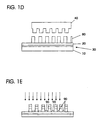
- the mold 40 then leaves the solidified polymeric material 70 on the transfer layer 20 , as shown in FIG. 1d .
- the transfer layer 20 is then selectively etched relative to the solid polymeric material 70 such that a relief image 80 corresponding to the image in mold 40 is formed in the transfer layer 20 .
- the etching step is depicted by FIG. 1c .
- the etching selectivity of the transfer layer 20 relative to the solid polymeric material 70 preferably ranges from about 1.5 to about 100.
- the selective etching or ion milling may be carried out may be carried out by subjecting the transfer layer 20 and the solid polymeric material 70 to an environment such as, but not limited to, an argon ion stream, an oxygen-containing plasma, a reactive ion etching gas, a halogen-containing gas, a sulfur dioxide-containing gas, and combinations of the above.
- an environment such as, but not limited to, an argon ion stream, an oxygen-containing plasma, a reactive ion etching gas, a halogen-containing gas, a sulfur dioxide-containing gas, and combinations of the above.
Landscapes
- Engineering & Computer Science (AREA)
- Nanotechnology (AREA)
- Chemical & Material Sciences (AREA)
- Physics & Mathematics (AREA)
- Mechanical Engineering (AREA)
- General Physics & Mathematics (AREA)
- Crystallography & Structural Chemistry (AREA)
- Theoretical Computer Science (AREA)
- Mathematical Physics (AREA)
- Condensed Matter Physics & Semiconductors (AREA)
- Manufacturing & Machinery (AREA)
- Shaping Of Tube Ends By Bending Or Straightening (AREA)
- Exposure Of Semiconductors, Excluding Electron Or Ion Beam Exposure (AREA)
- Moulds For Moulding Plastics Or The Like (AREA)
- Transition And Organic Metals Composition Catalysts For Addition Polymerization (AREA)
- Organic Low-Molecular-Weight Compounds And Preparation Thereof (AREA)
- Micromachines (AREA)
- Drying Of Semiconductors (AREA)
Claims (16)
- Verfahren zur Bildung eines Reliefbildes in einer Struktur, die ein Substrat und eine darauf gebildete Transferschicht umfasst, wobei dieses Verfahren umfasst:Bedeckung der Transferschicht mit einer polymerisierbaren flüssigen Zusammensetzung; in Kontakt bringen der polymerisierbaren flüssigen Zusammensetzung mit einer Form, die eine darin ausgebildete Reliefstruktur besitzt, so dass die polymerisierbare flüssige Zusammensetzung im Wesentlichen die Reliefstruktur in der Form ausfüllt;Unterwerfen der polymerisierbaren flüssigen Zusammensetzungen Bedingungen, um die polymerisierbare flüssige Zusammensetzung zu polymerisieren und daraus ein verfestigtes Polymermaterial auf der Transferschicht auszubilden;Abtrennung der Form vom festen Polymermaterial, so dass ein Abdruck der Reliefstruktur aus der Form in dem verfestigten Polymermaterial gebildet wird; undAussetzen der Transferschicht und des verfestigten Polymermaterials einer Umgebung, um selektiv die Transferschicht relativ zu dem verfestigten Polymermaterial derart zu ätzen, dass ein Reliefbild in der Transferschicht gebildet wird.
- Verfahren gemäß Anspruch 1, das weiterhin den Schritt der Fertigung einer Vorrichtung aus der Struktur umfasst, wobei die Vorrichtung ausgewählt ist aus einer mikroelektronischen Vorrichtung, einer Informationsspeicher-Vorrichtung, einer Leiterplatte, einem Flachbildschirm, einer Mikromaschine und einem Ladungskopplungsspeicher.
- Verfahren gemäß Anspruch 1 oder 2, worin die polymerisierbare flüssige Zusammensetzung ein Silizium enthaltendes Material oder ein Organosilan umfasst.
- Verfahren gemäß Anspruch 3, worin das Organosilan elementares Silizium in einer Menge enthält, die größer ist als ungefähr 8 Gewichtsprozent, bezogen auf das Gewicht der polymerisierbaren flüssigen Zusammensetzung.
- Verfahren gemäß irgendeinem der vorangehenden Ansprüche, worin die polymerisierbare flüssige Zusammensetzung eine reaktive Seitengruppe einschließt, ausgewählt aus einer Epoxygruppe, einer Ketenacetylgruppe, einer Acrylatgruppe, einer Methacrylatgruppe und deren Kombinationen.
- Verfahren gemäß irgendeinem der vorangehenden Ansprüche, worin die Transferschicht ein Material umfasst, ausgewählt aus einem organischen duroplastischen Polymer, einem thermoplastischen Polymer, einem Polyepoxy, einem Polyamid, einem Polyurethan, einem Polycarbonat, einem Polyester und deren Kombinationen.
- Verfahren gemäß irgendeinem der vorangehenden Ansprüche, worin die Form ein Material umfasst, ausgewählt aus Metall, Silizium, einem organischen Polymer, einem Siloxan-Polymer, Borosilicatglas, einem Fluorcarbon-Polymer und deren Kombinationen.
- Verfahren gemäß irgendeinem der vorangehenden Ansprüche, worin die Form Quarz umfasst.
- Verfahren gemäß irgendeinem der vorangehenden Ansprüche, das weiterhin den Schritt der Behandlung der Form mit einem oberflächenmodifizierenden Agens umfasst.
- Verfahren gemäß Anspruch 9, worin das oberflächenmodifizierende Agens ein Fluorkohlenwasserstoff-Silylierungsmittel ist.
- Verfahren gemäß Anspruch 9 oder Anspruch 10, worin der genannte Schritt der Behandlung der Form durchgeführt wird, indem eine Technik angewandt wird, ausgewählt aus einer Plasma-Technik, einer chemischen Aufdampfungs-Technik, einer Lösungsglühungs-Technik und deren Mischungen.
- Verfahren gemäß irgendeinem der vorangehenden Ansprüche, worin die Form transparent ist und worin der genannte Schritt des Unterwerfens der polymerisierbaren flüssigen Zusammensetzung umfasst, dass man die polymerisierbare flüssige Zusammensetzung Strahlung unterwirft, die ausreichend ist, um die flüssige Zusammensetzung zu polymerisieren und ein festes Polymermaterial zu bilden.
- Verfahren gemäß irgendeinem der vorangehenden Ansprüche, worin der genannte Schritt der Aussetzung der Transferschicht und des festen Polymermaterials einer Umgebung umfasst, dass man die Transferschicht und das feste Polymermaterial einer Umgebung aussetzt, die einen Argonionenstrom, ein Sauerstoff-enthaltendes Plasma, ein reaktives Ionenätzgas, ein Halogen enthaltendes Gas, ein Schwefeldioxid enthaltendes Gas und deren Kombinationen umfasst.
- Verfahren gemäß irgendeinem der vorangehenden Ansprüche, worin das Restmaterial, ausgewählt aus einem Anteil der polymerisierbaren flüssigen Zusammensetzung, einem Anteil des festen Polymermaterials und deren Kombinationen im Anschluss an den genannten Schritt vorliegt, bei dem man die polymerisierbare flüssige Zusammensetzung Bedingungen unterwirft, um ein festes Polymermaterial zu bilden, und das genannte Verfahren weiterhin den Schritt umfasst, bei dem das Restmaterial Bedingungen unterworfen wird, so dass das Restmaterial entfernt wird.
- Verfahren gemäß Anspruch 14, worin der genannte Schritt des Unterwerfens des Restmaterials vor dem genannten Schritt erfolgt, bei dem man die Transferschicht und das feste Polymermaterial einer Umwelt aussetzt, um selektiv die Transferschicht relativ zu dem festen Polymermaterial zu ätzen.
- Verfahren gemäß Anspruch 14 oder Anspruch 15, worin der genannte Schritt, bei dem man das Restmaterial Bedingungen aussetzt, so dass das Restmaterial entfernt wird, umfasst, dass man das Restmaterial einer Umgebung aussetzt, die ausgewählt ist aus einem Argonionenstrom, einem Fluorid enthaltenden Plasma, einem reaktiven Ionenätzgas und deren Mischungen.
Applications Claiming Priority (3)
| Application Number | Priority Date | Filing Date | Title |
|---|---|---|---|
| US09/266,663 US6334960B1 (en) | 1999-03-11 | 1999-03-11 | Step and flash imprint lithography |
| US266663 | 1999-03-11 | ||
| PCT/US2000/005751 WO2000054107A1 (en) | 1999-03-11 | 2000-03-03 | Step and flash imprint lithography |
Publications (2)
| Publication Number | Publication Date |
|---|---|
| EP1228401A1 EP1228401A1 (de) | 2002-08-07 |
| EP1228401B1 true EP1228401B1 (de) | 2005-08-10 |
Family
ID=23015492
Family Applications (1)
| Application Number | Title | Priority Date | Filing Date |
|---|---|---|---|
| EP00913745A Expired - Lifetime EP1228401B1 (de) | 1999-03-11 | 2000-03-03 | Prägeform-lithographie |
Country Status (6)
| Country | Link |
|---|---|
| US (4) | US6334960B1 (de) |
| EP (1) | EP1228401B1 (de) |
| JP (1) | JP2002539604A (de) |
| AT (1) | ATE301846T1 (de) |
| DE (1) | DE60021909T2 (de) |
| WO (1) | WO2000054107A1 (de) |
Cited By (1)
| Publication number | Priority date | Publication date | Assignee | Title |
|---|---|---|---|---|
| CN111448485A (zh) * | 2017-10-30 | 2020-07-24 | 脸谱科技有限责任公司 | 高折射率材料的h2辅助的倾斜蚀刻 |
Families Citing this family (426)
| Publication number | Priority date | Publication date | Assignee | Title |
|---|---|---|---|---|
| US8128856B2 (en) * | 1995-11-15 | 2012-03-06 | Regents Of The University Of Minnesota | Release surfaces, particularly for use in nanoimprint lithography |
| US20040137734A1 (en) * | 1995-11-15 | 2004-07-15 | Princeton University | Compositions and processes for nanoimprinting |
| US6334960B1 (en) * | 1999-03-11 | 2002-01-01 | Board Of Regents, The University Of Texas System | Step and flash imprint lithography |
| US6780001B2 (en) * | 1999-07-30 | 2004-08-24 | Formfactor, Inc. | Forming tool for forming a contoured microelectronic spring mold |
| US6939474B2 (en) * | 1999-07-30 | 2005-09-06 | Formfactor, Inc. | Method for forming microelectronic spring structures on a substrate |
| US6873087B1 (en) | 1999-10-29 | 2005-03-29 | Board Of Regents, The University Of Texas System | High precision orientation alignment and gap control stages for imprint lithography processes |
| US7432634B2 (en) | 2000-10-27 | 2008-10-07 | Board Of Regents, University Of Texas System | Remote center compliant flexure device |
| SE516194C2 (sv) * | 2000-04-18 | 2001-12-03 | Obducat Ab | Substrat för samt process vid tillverkning av strukturer |
| KR100862301B1 (ko) | 2000-07-16 | 2008-10-13 | 보드 오브 리전츠, 더 유니버시티 오브 텍사스 시스템 | 임프린트 리소그래피를 위한 고분해능 오버레이 정렬 방법 및 시스템 |
| EP2270592B1 (de) * | 2000-07-17 | 2015-09-02 | Board of Regents, The University of Texas System | Verfahren zur Bildung einer Struktur auf einem Substrat |
| US20050160011A1 (en) * | 2004-01-20 | 2005-07-21 | Molecular Imprints, Inc. | Method for concurrently employing differing materials to form a layer on a substrate |
| CN1696826A (zh) | 2000-08-01 | 2005-11-16 | 得克萨斯州大学系统董事会 | 用对激活光透明的模板在衬底上形成图案的方法及半导体器件 |
| US8016277B2 (en) * | 2000-08-21 | 2011-09-13 | Board Of Regents, The University Of Texas System | Flexure based macro motion translation stage |
| EP1352295B1 (de) * | 2000-10-12 | 2015-12-23 | Board of Regents, The University of Texas System | Schablone für die mikro- und nanodrucklithographie für zimmertemperatur und niedrigen druck |
| US20050274219A1 (en) * | 2004-06-01 | 2005-12-15 | Molecular Imprints, Inc. | Method and system to control movement of a body for nano-scale manufacturing |
| US20060005657A1 (en) * | 2004-06-01 | 2006-01-12 | Molecular Imprints, Inc. | Method and system to control movement of a body for nano-scale manufacturing |
| US6964793B2 (en) * | 2002-05-16 | 2005-11-15 | Board Of Regents, The University Of Texas System | Method for fabricating nanoscale patterns in light curable compositions using an electric field |
| SE519573C2 (sv) | 2001-07-05 | 2003-03-11 | Obducat Ab | Stamp med antividhäftningsskikt samt sätt att framställa och sätt att reparera en sådan stamp |
| WO2003010289A2 (en) * | 2001-07-25 | 2003-02-06 | The Trustees Of Princeton University | Nanochannel arrays and their preparation and use for high throughput macromolecular analysis |
| US9678038B2 (en) | 2001-07-25 | 2017-06-13 | The Trustees Of Princeton University | Nanochannel arrays and their preparation and use for high throughput macromolecular analysis |
| JP2003109915A (ja) * | 2001-09-28 | 2003-04-11 | National Institute Of Advanced Industrial & Technology | 剥離性雰囲気でのインプリントリソグラフィー方法及び装置 |
| EP1441868A4 (de) * | 2001-10-11 | 2006-08-30 | Brewer Science Inc | Reproduktion von gemusterter struktur unter verwendung von nichthaftender form |
| US20030071016A1 (en) | 2001-10-11 | 2003-04-17 | Wu-Sheng Shih | Patterned structure reproduction using nonsticking mold |
| KR20030057067A (ko) * | 2001-12-28 | 2003-07-04 | 엘지.필립스 엘시디 주식회사 | 인쇄방식을 이용한 패턴형성방법 |
| JP2003218658A (ja) * | 2002-01-17 | 2003-07-31 | Nec Corp | 弾性表面波素子及び半導体装置の製造方法 |
| US20030186405A1 (en) * | 2002-04-01 | 2003-10-02 | The Ohio State University Research Foundation | Micro/nano-embossing process and useful applications thereof |
| US7652574B2 (en) * | 2002-04-08 | 2010-01-26 | Sayegh Adel O | Article surveillance tag having a vial |
| AU2003269813A1 (en) | 2002-04-16 | 2003-12-31 | Princeton University | Gradient structures interfacing microfluidics and nanofluidics, methods for fabrication and uses thereof |
| US6730617B2 (en) | 2002-04-24 | 2004-05-04 | Ibm | Method of fabricating one or more tiers of an integrated circuit |
| US7037639B2 (en) * | 2002-05-01 | 2006-05-02 | Molecular Imprints, Inc. | Methods of manufacturing a lithography template |
| US20030235787A1 (en) * | 2002-06-24 | 2003-12-25 | Watts Michael P.C. | Low viscosity high resolution patterning material |
| US7179079B2 (en) * | 2002-07-08 | 2007-02-20 | Molecular Imprints, Inc. | Conforming template for patterning liquids disposed on substrates |
| US20080160129A1 (en) * | 2006-05-11 | 2008-07-03 | Molecular Imprints, Inc. | Template Having a Varying Thickness to Facilitate Expelling a Gas Positioned Between a Substrate and the Template |
| US6926929B2 (en) * | 2002-07-09 | 2005-08-09 | Molecular Imprints, Inc. | System and method for dispensing liquids |
| US6900881B2 (en) * | 2002-07-11 | 2005-05-31 | Molecular Imprints, Inc. | Step and repeat imprint lithography systems |
| US6908861B2 (en) * | 2002-07-11 | 2005-06-21 | Molecular Imprints, Inc. | Method for imprint lithography using an electric field |
| US7442336B2 (en) * | 2003-08-21 | 2008-10-28 | Molecular Imprints, Inc. | Capillary imprinting technique |
| US7077992B2 (en) | 2002-07-11 | 2006-07-18 | Molecular Imprints, Inc. | Step and repeat imprint lithography processes |
| US7019819B2 (en) * | 2002-11-13 | 2006-03-28 | Molecular Imprints, Inc. | Chucking system for modulating shapes of substrates |
| US6932934B2 (en) | 2002-07-11 | 2005-08-23 | Molecular Imprints, Inc. | Formation of discontinuous films during an imprint lithography process |
| MY164487A (en) * | 2002-07-11 | 2017-12-29 | Molecular Imprints Inc | Step and repeat imprint lithography processes |
| US7027156B2 (en) * | 2002-08-01 | 2006-04-11 | Molecular Imprints, Inc. | Scatterometry alignment for imprint lithography |
| US6916584B2 (en) | 2002-08-01 | 2005-07-12 | Molecular Imprints, Inc. | Alignment methods for imprint lithography |
| US7070405B2 (en) * | 2002-08-01 | 2006-07-04 | Molecular Imprints, Inc. | Alignment systems for imprint lithography |
| US7071088B2 (en) * | 2002-08-23 | 2006-07-04 | Molecular Imprints, Inc. | Method for fabricating bulbous-shaped vias |
| US6936194B2 (en) * | 2002-09-05 | 2005-08-30 | Molecular Imprints, Inc. | Functional patterning material for imprint lithography processes |
| US8349241B2 (en) * | 2002-10-04 | 2013-01-08 | Molecular Imprints, Inc. | Method to arrange features on a substrate to replicate features having minimal dimensional variability |
| US20040065252A1 (en) * | 2002-10-04 | 2004-04-08 | Sreenivasan Sidlgata V. | Method of forming a layer on a substrate to facilitate fabrication of metrology standards |
| DE60333715D1 (de) * | 2002-10-30 | 2010-09-23 | Hitachi Ltd | Verfahren zur Herstellung funktioneller Substrate, die kolumnare Mikrosäulen aufweisen |
| AU2003291443A1 (en) * | 2002-11-12 | 2004-06-03 | Princeton University | Compositions and processes for nanoimprinting |
| ATE438197T1 (de) | 2002-11-13 | 2009-08-15 | Molecular Imprints Inc | Ein halterungssystem und ein verfahren zum modulieren von substratformen |
| US6929762B2 (en) * | 2002-11-13 | 2005-08-16 | Molecular Imprints, Inc. | Method of reducing pattern distortions during imprint lithography processes |
| US6980282B2 (en) * | 2002-12-11 | 2005-12-27 | Molecular Imprints, Inc. | Method for modulating shapes of substrates |
| US7641840B2 (en) * | 2002-11-13 | 2010-01-05 | Molecular Imprints, Inc. | Method for expelling gas positioned between a substrate and a mold |
| US6900126B2 (en) | 2002-11-20 | 2005-05-31 | International Business Machines Corporation | Method of forming metallized pattern |
| US7365103B2 (en) * | 2002-12-12 | 2008-04-29 | Board Of Regents, The University Of Texas System | Compositions for dark-field polymerization and method of using the same for imprint lithography processes |
| US20040112862A1 (en) * | 2002-12-12 | 2004-06-17 | Molecular Imprints, Inc. | Planarization composition and method of patterning a substrate using the same |
| US6871558B2 (en) * | 2002-12-12 | 2005-03-29 | Molecular Imprints, Inc. | Method for determining characteristics of substrate employing fluid geometries |
| TW200500811A (en) * | 2002-12-13 | 2005-01-01 | Molecular Imprints Inc | Magnification correction employing out-of-plane distortion of a substrate |
| JP2004241397A (ja) * | 2003-01-23 | 2004-08-26 | Dainippon Printing Co Ltd | 薄膜トランジスタおよびその製造方法 |
| US7452574B2 (en) | 2003-02-27 | 2008-11-18 | Molecular Imprints, Inc. | Method to reduce adhesion between a polymerizable layer and a substrate employing a fluorine-containing layer |
| US20040168613A1 (en) * | 2003-02-27 | 2004-09-02 | Molecular Imprints, Inc. | Composition and method to form a release layer |
| JP4317375B2 (ja) * | 2003-03-20 | 2009-08-19 | 株式会社日立製作所 | ナノプリント装置、及び微細構造転写方法 |
| US7323417B2 (en) * | 2004-09-21 | 2008-01-29 | Molecular Imprints, Inc. | Method of forming a recessed structure employing a reverse tone process |
| US7179396B2 (en) * | 2003-03-25 | 2007-02-20 | Molecular Imprints, Inc. | Positive tone bi-layer imprint lithography method |
| US7122079B2 (en) * | 2004-02-27 | 2006-10-17 | Molecular Imprints, Inc. | Composition for an etching mask comprising a silicon-containing material |
| US7186656B2 (en) * | 2004-05-21 | 2007-03-06 | Molecular Imprints, Inc. | Method of forming a recessed structure employing a reverse tone process |
| US20040202865A1 (en) * | 2003-04-08 | 2004-10-14 | Andrew Homola | Release coating for stamper |
| US7410904B2 (en) * | 2003-04-24 | 2008-08-12 | Hewlett-Packard Development Company, L.P. | Sensor produced using imprint lithography |
| US7396475B2 (en) * | 2003-04-25 | 2008-07-08 | Molecular Imprints, Inc. | Method of forming stepped structures employing imprint lithography |
| US6951173B1 (en) * | 2003-05-14 | 2005-10-04 | Molecular Imprints, Inc. | Assembly and method for transferring imprint lithography templates |
| US6805054B1 (en) * | 2003-05-14 | 2004-10-19 | Molecular Imprints, Inc. | Method, system and holder for transferring templates during imprint lithography processes |
| ATE487579T1 (de) * | 2003-05-14 | 2010-11-15 | Molecular Imprints Inc | Verfahren, system, halter und anordnung zur übertragung von templates bei imprint- lithographieverfahren |
| US20050160934A1 (en) * | 2004-01-23 | 2005-07-28 | Molecular Imprints, Inc. | Materials and methods for imprint lithography |
| US20060108710A1 (en) * | 2004-11-24 | 2006-05-25 | Molecular Imprints, Inc. | Method to reduce adhesion between a conformable region and a mold |
| US7307118B2 (en) * | 2004-11-24 | 2007-12-11 | Molecular Imprints, Inc. | Composition to reduce adhesion between a conformable region and a mold |
| US7157036B2 (en) * | 2003-06-17 | 2007-01-02 | Molecular Imprints, Inc | Method to reduce adhesion between a conformable region and a pattern of a mold |
| US7150622B2 (en) * | 2003-07-09 | 2006-12-19 | Molecular Imprints, Inc. | Systems for magnification and distortion correction for imprint lithography processes |
| KR100606532B1 (ko) * | 2003-08-02 | 2006-07-31 | 동부일렉트로닉스 주식회사 | 반도체 소자의 제조 방법 |
| DE10340608A1 (de) | 2003-08-29 | 2005-03-24 | Infineon Technologies Ag | Polymerformulierung und Verfahren zur Herstellung einer Dielektrikumsschicht |
| WO2005030822A2 (en) * | 2003-09-23 | 2005-04-07 | University Of North Carolina At Chapel Hill | Photocurable perfluoropolyethers for use as novel materials in microfluidic devices |
| US7136150B2 (en) * | 2003-09-25 | 2006-11-14 | Molecular Imprints, Inc. | Imprint lithography template having opaque alignment marks |
| US7090716B2 (en) * | 2003-10-02 | 2006-08-15 | Molecular Imprints, Inc. | Single phase fluid imprint lithography method |
| US8211214B2 (en) * | 2003-10-02 | 2012-07-03 | Molecular Imprints, Inc. | Single phase fluid imprint lithography method |
| US7261830B2 (en) * | 2003-10-16 | 2007-08-28 | Molecular Imprints, Inc. | Applying imprinting material to substrates employing electromagnetic fields |
| US20050084804A1 (en) * | 2003-10-16 | 2005-04-21 | Molecular Imprints, Inc. | Low surface energy templates |
| US7122482B2 (en) * | 2003-10-27 | 2006-10-17 | Molecular Imprints, Inc. | Methods for fabricating patterned features utilizing imprint lithography |
| US20050106321A1 (en) * | 2003-11-14 | 2005-05-19 | Molecular Imprints, Inc. | Dispense geometery to achieve high-speed filling and throughput |
| US20050098534A1 (en) * | 2003-11-12 | 2005-05-12 | Molecular Imprints, Inc. | Formation of conductive templates employing indium tin oxide |
| EP1538482B1 (de) * | 2003-12-05 | 2016-02-17 | Obducat AB | Gerät und Methode für grossflÀ¤chige Lithographie |
| US9040090B2 (en) * | 2003-12-19 | 2015-05-26 | The University Of North Carolina At Chapel Hill | Isolated and fixed micro and nano structures and methods thereof |
| US8263129B2 (en) | 2003-12-19 | 2012-09-11 | The University Of North Carolina At Chapel Hill | Methods for fabricating isolated micro-and nano-structures using soft or imprint lithography |
| KR101010431B1 (ko) * | 2003-12-27 | 2011-01-21 | 엘지디스플레이 주식회사 | 평판표시소자의 제조방법 및 장치 |
| US20050156353A1 (en) * | 2004-01-15 | 2005-07-21 | Watts Michael P. | Method to improve the flow rate of imprinting material |
| US20050158419A1 (en) * | 2004-01-15 | 2005-07-21 | Watts Michael P. | Thermal processing system for imprint lithography |
| US7462292B2 (en) * | 2004-01-27 | 2008-12-09 | Hewlett-Packard Development Company, L.P. | Silicon carbide imprint stamp |
| US7060625B2 (en) * | 2004-01-27 | 2006-06-13 | Hewlett-Packard Development Company, L.P. | Imprint stamp |
| WO2005084191A2 (en) * | 2004-02-13 | 2005-09-15 | The University Of North Carolina At Chapel Hill | Functional materials and novel methods for the fabrication of microfluidic devices |
| US7019835B2 (en) * | 2004-02-19 | 2006-03-28 | Molecular Imprints, Inc. | Method and system to measure characteristics of a film disposed on a substrate |
| US8076386B2 (en) * | 2004-02-23 | 2011-12-13 | Molecular Imprints, Inc. | Materials for imprint lithography |
| US20050189676A1 (en) * | 2004-02-27 | 2005-09-01 | Molecular Imprints, Inc. | Full-wafer or large area imprinting with multiple separated sub-fields for high throughput lithography |
| US7906180B2 (en) * | 2004-02-27 | 2011-03-15 | Molecular Imprints, Inc. | Composition for an etching mask comprising a silicon-containing material |
| US7730834B2 (en) * | 2004-03-04 | 2010-06-08 | Asml Netherlands B.V. | Printing apparatus and device manufacturing method |
| JP4481698B2 (ja) | 2004-03-29 | 2010-06-16 | キヤノン株式会社 | 加工装置 |
| JP4393244B2 (ja) * | 2004-03-29 | 2010-01-06 | キヤノン株式会社 | インプリント装置 |
| DE102004028851B4 (de) * | 2004-03-31 | 2006-04-13 | Infineon Technologies Ag | Verfahren und Vorrichtung zum Vermessen eines Oberflächenprofils einer Probe |
| US20050230882A1 (en) * | 2004-04-19 | 2005-10-20 | Molecular Imprints, Inc. | Method of forming a deep-featured template employed in imprint lithography |
| US8235302B2 (en) * | 2004-04-20 | 2012-08-07 | Nanolnk, Inc. | Identification features |
| US7140861B2 (en) * | 2004-04-27 | 2006-11-28 | Molecular Imprints, Inc. | Compliant hard template for UV imprinting |
| US20080055581A1 (en) * | 2004-04-27 | 2008-03-06 | Rogers John A | Devices and methods for pattern generation by ink lithography |
| JP2008507114A (ja) * | 2004-04-27 | 2008-03-06 | ザ ボード オブ トラスティーズ オブ ザ ユニヴァーシティー オブ イリノイ | ソフトリソグラフィ用複合パターニングデバイス |
| EP1594001B1 (de) * | 2004-05-07 | 2015-12-30 | Obducat AB | Gerät und Verfahren für die Imprint-Lithographie |
| US20050253307A1 (en) * | 2004-05-11 | 2005-11-17 | Molecualr Imprints, Inc. | Method of patterning a conductive layer on a substrate |
| US7307697B2 (en) * | 2004-05-28 | 2007-12-11 | Board Of Regents, The University Of Texas System | Adaptive shape substrate support system |
| US20050275311A1 (en) * | 2004-06-01 | 2005-12-15 | Molecular Imprints, Inc. | Compliant device for nano-scale manufacturing |
| US20050276919A1 (en) * | 2004-06-01 | 2005-12-15 | Molecular Imprints, Inc. | Method for dispensing a fluid on a substrate |
| US20050270516A1 (en) * | 2004-06-03 | 2005-12-08 | Molecular Imprints, Inc. | System for magnification and distortion correction during nano-scale manufacturing |
| ATE477515T1 (de) * | 2004-06-03 | 2010-08-15 | Molecular Imprints Inc | Fluidausgabe und tropfenausgabe nach bedarf für die herstellung im nanobereich |
| EP2650907B1 (de) | 2004-06-04 | 2024-10-23 | The Board Of Trustees Of The University Of Illinois | Verfahren und Einrichtungen zum Herstellen und Zusammenbauen von druckbaren Halbleiterelementen |
| US7799699B2 (en) | 2004-06-04 | 2010-09-21 | The Board Of Trustees Of The University Of Illinois | Printable semiconductor structures and related methods of making and assembling |
| US7943491B2 (en) * | 2004-06-04 | 2011-05-17 | The Board Of Trustees Of The University Of Illinois | Pattern transfer printing by kinetic control of adhesion to an elastomeric stamp |
| US7521292B2 (en) | 2004-06-04 | 2009-04-21 | The Board Of Trustees Of The University Of Illinois | Stretchable form of single crystal silicon for high performance electronics on rubber substrates |
| US20050272599A1 (en) * | 2004-06-04 | 2005-12-08 | Kenneth Kramer | Mold release layer |
| US20050277066A1 (en) * | 2004-06-10 | 2005-12-15 | Le Ngoc V | Selective etch process for step and flash imprint lithography |
| US20070228593A1 (en) * | 2006-04-03 | 2007-10-04 | Molecular Imprints, Inc. | Residual Layer Thickness Measurement and Correction |
| JP2006013400A (ja) * | 2004-06-29 | 2006-01-12 | Canon Inc | 2つの対象物間の相対的位置ずれ検出方法及び装置 |
| US7785526B2 (en) * | 2004-07-20 | 2010-08-31 | Molecular Imprints, Inc. | Imprint alignment method, system, and template |
| US20060017876A1 (en) * | 2004-07-23 | 2006-01-26 | Molecular Imprints, Inc. | Displays and method for fabricating displays |
| US8088293B2 (en) | 2004-07-29 | 2012-01-03 | Micron Technology, Inc. | Methods of forming reticles configured for imprint lithography |
| US7105452B2 (en) * | 2004-08-13 | 2006-09-12 | Molecular Imprints, Inc. | Method of planarizing a semiconductor substrate with an etching chemistry |
| US7309225B2 (en) * | 2004-08-13 | 2007-12-18 | Molecular Imprints, Inc. | Moat system for an imprint lithography template |
| US7282550B2 (en) * | 2004-08-16 | 2007-10-16 | Molecular Imprints, Inc. | Composition to provide a layer with uniform etch characteristics |
| US7939131B2 (en) * | 2004-08-16 | 2011-05-10 | Molecular Imprints, Inc. | Method to provide a layer with uniform etch characteristics |
| US20070164476A1 (en) * | 2004-09-01 | 2007-07-19 | Wei Wu | Contact lithography apparatus and method employing substrate deformation |
| US7641468B2 (en) * | 2004-09-01 | 2010-01-05 | Hewlett-Packard Development Company, L.P. | Imprint lithography apparatus and method employing an effective pressure |
| US7252777B2 (en) * | 2004-09-21 | 2007-08-07 | Molecular Imprints, Inc. | Method of forming an in-situ recessed structure |
| SG147417A1 (en) * | 2004-09-21 | 2008-11-28 | Molecular Imprints Inc | Method of forming an in-situ recessed structure |
| US7041604B2 (en) * | 2004-09-21 | 2006-05-09 | Molecular Imprints, Inc. | Method of patterning surfaces while providing greater control of recess anisotropy |
| US7205244B2 (en) * | 2004-09-21 | 2007-04-17 | Molecular Imprints | Patterning substrates employing multi-film layers defining etch-differential interfaces |
| US7241395B2 (en) * | 2004-09-21 | 2007-07-10 | Molecular Imprints, Inc. | Reverse tone patterning on surfaces having planarity perturbations |
| US7547504B2 (en) * | 2004-09-21 | 2009-06-16 | Molecular Imprints, Inc. | Pattern reversal employing thick residual layers |
| US20060062922A1 (en) * | 2004-09-23 | 2006-03-23 | Molecular Imprints, Inc. | Polymerization technique to attenuate oxygen inhibition of solidification of liquids and composition therefor |
| US7244386B2 (en) * | 2004-09-27 | 2007-07-17 | Molecular Imprints, Inc. | Method of compensating for a volumetric shrinkage of a material disposed upon a substrate to form a substantially planar structure therefrom |
| US8147742B2 (en) * | 2004-10-08 | 2012-04-03 | Dow Corning Corporation | Lithography processes using phase change compositions |
| US20060081557A1 (en) | 2004-10-18 | 2006-04-20 | Molecular Imprints, Inc. | Low-k dielectric functional imprinting materials |
| US7163888B2 (en) * | 2004-11-22 | 2007-01-16 | Motorola, Inc. | Direct imprinting of etch barriers using step and flash imprint lithography |
| US7630067B2 (en) | 2004-11-30 | 2009-12-08 | Molecular Imprints, Inc. | Interferometric analysis method for the manufacture of nano-scale devices |
| US20070231421A1 (en) * | 2006-04-03 | 2007-10-04 | Molecular Imprints, Inc. | Enhanced Multi Channel Alignment |
| WO2006059580A1 (ja) | 2004-11-30 | 2006-06-08 | Asahi Glass Company, Limited | モールド、および転写微細パターンを有する基材の製造方法 |
| US7292326B2 (en) * | 2004-11-30 | 2007-11-06 | Molecular Imprints, Inc. | Interferometric analysis for the manufacture of nano-scale devices |
| WO2006060757A2 (en) * | 2004-12-01 | 2006-06-08 | Molecular Imprints, Inc. | Eliminating printability of sub-resolution defects in imprint lithography |
| JP5198071B2 (ja) * | 2004-12-01 | 2013-05-15 | モレキュラー・インプリンツ・インコーポレーテッド | インプリントリソグラフィ・プロセスにおける熱管理のための露光方法 |
| US7811505B2 (en) | 2004-12-07 | 2010-10-12 | Molecular Imprints, Inc. | Method for fast filling of templates for imprint lithography using on template dispense |
| CN100468814C (zh) * | 2004-12-15 | 2009-03-11 | 鸿富锦精密工业(深圳)有限公司 | 有机发光显示器 |
| US7125495B2 (en) * | 2004-12-20 | 2006-10-24 | Palo Alto Research Center, Inc. | Large area electronic device with high and low resolution patterned film features |
| US7676088B2 (en) * | 2004-12-23 | 2010-03-09 | Asml Netherlands B.V. | Imprint lithography |
| US20060144274A1 (en) * | 2004-12-30 | 2006-07-06 | Asml Netherlands B.V. | Imprint lithography |
| US20060145398A1 (en) * | 2004-12-30 | 2006-07-06 | Board Of Regents, The University Of Texas System | Release layer comprising diamond-like carbon (DLC) or doped DLC with tunable composition for imprint lithography templates and contact masks |
| US7490547B2 (en) * | 2004-12-30 | 2009-02-17 | Asml Netherlands B.V. | Imprint lithography |
| US7686970B2 (en) * | 2004-12-30 | 2010-03-30 | Asml Netherlands B.V. | Imprint lithography |
| US20060144814A1 (en) * | 2004-12-30 | 2006-07-06 | Asml Netherlands B.V. | Imprint lithography |
| US7354698B2 (en) * | 2005-01-07 | 2008-04-08 | Asml Netherlands B.V. | Imprint lithography |
| US20070299176A1 (en) * | 2005-01-28 | 2007-12-27 | Markley Thomas J | Photodefinable low dielectric constant material and method for making and using same |
| US7635263B2 (en) * | 2005-01-31 | 2009-12-22 | Molecular Imprints, Inc. | Chucking system comprising an array of fluid chambers |
| US20060177535A1 (en) * | 2005-02-04 | 2006-08-10 | Molecular Imprints, Inc. | Imprint lithography template to facilitate control of liquid movement |
| US7636999B2 (en) * | 2005-01-31 | 2009-12-29 | Molecular Imprints, Inc. | Method of retaining a substrate to a wafer chuck |
| CN101156107B (zh) * | 2005-02-03 | 2010-11-24 | 北卡罗来纳大学查珀尔希尔分校 | 用于液晶显示器的低表面能聚合物材料 |
| US7922474B2 (en) * | 2005-02-17 | 2011-04-12 | Asml Netherlands B.V. | Imprint lithography |
| US8097400B2 (en) * | 2005-02-22 | 2012-01-17 | Hewlett-Packard Development Company, L.P. | Method for forming an electronic device |
| JP2006245072A (ja) * | 2005-02-28 | 2006-09-14 | Canon Inc | パターン転写用モールドおよび転写装置 |
| US7277619B2 (en) * | 2005-03-04 | 2007-10-02 | Hewlett-Packard Development Company, L.P. | Nano-imprinted photonic crystal waveguide |
| US7523701B2 (en) * | 2005-03-07 | 2009-04-28 | Asml Netherlands B.V. | Imprint lithography method and apparatus |
| EP1700680A1 (de) * | 2005-03-09 | 2006-09-13 | EPFL Ecole Polytechnique Fédérale de Lausanne | Die Entformung erleichternde Formwerkzeuge aus Fluorpolymer zur Reproduktion von Nano- und Mikromustern |
| US7762186B2 (en) * | 2005-04-19 | 2010-07-27 | Asml Netherlands B.V. | Imprint lithography |
| US7611348B2 (en) * | 2005-04-19 | 2009-11-03 | Asml Netherlands B.V. | Imprint lithography |
| WO2006114958A1 (ja) * | 2005-04-21 | 2006-11-02 | Asahi Glass Company, Limited | 光硬化性組成物、微細パターン形成体およびその製造方法 |
| US8092959B2 (en) * | 2005-04-27 | 2012-01-10 | Obducat Ab | Means for transferring a pattern to an object |
| JP4736522B2 (ja) * | 2005-04-28 | 2011-07-27 | 旭硝子株式会社 | エッチング処理された処理基板の製造方法 |
| JP4742665B2 (ja) * | 2005-04-28 | 2011-08-10 | 旭硝子株式会社 | エッチング処理された処理基板の製造方法 |
| US20070228608A1 (en) * | 2006-04-03 | 2007-10-04 | Molecular Imprints, Inc. | Preserving Filled Features when Vacuum Wiping |
| US7767129B2 (en) * | 2005-05-11 | 2010-08-03 | Micron Technology, Inc. | Imprint templates for imprint lithography, and methods of patterning a plurality of substrates |
| US7442029B2 (en) * | 2005-05-16 | 2008-10-28 | Asml Netherlands B.V. | Imprint lithography |
| US20060266916A1 (en) * | 2005-05-25 | 2006-11-30 | Molecular Imprints, Inc. | Imprint lithography template having a coating to reflect and/or absorb actinic energy |
| US20060267231A1 (en) * | 2005-05-27 | 2006-11-30 | Asml Netherlands B.V. | Imprint lithography |
| US7692771B2 (en) * | 2005-05-27 | 2010-04-06 | Asml Netherlands B.V. | Imprint lithography |
| US7708924B2 (en) * | 2005-07-21 | 2010-05-04 | Asml Netherlands B.V. | Imprint lithography |
| US7418902B2 (en) * | 2005-05-31 | 2008-09-02 | Asml Netherlands B.V. | Imprint lithography including alignment |
| KR101117987B1 (ko) * | 2005-06-07 | 2012-03-06 | 엘지디스플레이 주식회사 | 평판표시소자의 제조장치 및 방법 |
| JP3958344B2 (ja) * | 2005-06-07 | 2007-08-15 | キヤノン株式会社 | インプリント装置、インプリント方法及びチップの製造方法 |
| US7927089B2 (en) * | 2005-06-08 | 2011-04-19 | Canon Kabushiki Kaisha | Mold, apparatus including mold, pattern transfer apparatus, and pattern forming method |
| US7854873B2 (en) * | 2005-06-10 | 2010-12-21 | Obducat Ab | Imprint stamp comprising cyclic olefin copolymer |
| DE602005012068D1 (de) | 2005-06-10 | 2009-02-12 | Obducat Ab | Kopieren eines Musters mit Hilfe eines Zwischenstempels |
| US7377764B2 (en) * | 2005-06-13 | 2008-05-27 | Asml Netherlands B.V. | Imprint lithography |
| DE102005045331A1 (de) * | 2005-06-16 | 2006-12-28 | Süss MicroTec AG | Entfernen von dünnen strukturierten Polymerschichten durch atmosphärisches Plasma |
| US20060284156A1 (en) * | 2005-06-16 | 2006-12-21 | Thomas Happ | Phase change memory cell defined by imprint lithography |
| US7256131B2 (en) * | 2005-07-19 | 2007-08-14 | Molecular Imprints, Inc. | Method of controlling the critical dimension of structures formed on a substrate |
| US8557351B2 (en) * | 2005-07-22 | 2013-10-15 | Molecular Imprints, Inc. | Method for adhering materials together |
| US8808808B2 (en) | 2005-07-22 | 2014-08-19 | Molecular Imprints, Inc. | Method for imprint lithography utilizing an adhesion primer layer |
| US7759407B2 (en) * | 2005-07-22 | 2010-07-20 | Molecular Imprints, Inc. | Composition for adhering materials together |
| US8846195B2 (en) * | 2005-07-22 | 2014-09-30 | Canon Nanotechnologies, Inc. | Ultra-thin polymeric adhesion layer |
| US20070023976A1 (en) * | 2005-07-26 | 2007-02-01 | Asml Netherlands B.V. | Imprint lithography |
| WO2007133235A2 (en) * | 2005-08-08 | 2007-11-22 | Liquidia Technologies, Inc. | Micro and nano-structure metrology |
| EP1922364A4 (de) | 2005-08-09 | 2010-04-21 | Univ North Carolina | Verfahren und materialien zur herstellung mikrofluidischer vorrichtungen |
| US7766640B2 (en) * | 2005-08-12 | 2010-08-03 | Hewlett-Packard Development Company, L.P. | Contact lithography apparatus, system and method |
| US20070064384A1 (en) * | 2005-08-25 | 2007-03-22 | Molecular Imprints, Inc. | Method to transfer a template transfer body between a motion stage and a docking plate |
| US7665981B2 (en) * | 2005-08-25 | 2010-02-23 | Molecular Imprints, Inc. | System to transfer a template transfer body between a motion stage and a docking plate |
| US20070074635A1 (en) * | 2005-08-25 | 2007-04-05 | Molecular Imprints, Inc. | System to couple a body and a docking plate |
| KR100758699B1 (ko) * | 2005-08-29 | 2007-09-14 | 재단법인서울대학교산학협력재단 | 고종횡비 나노구조물 형성방법 및 이를 이용한 미세패턴형성방법 |
| US7488771B2 (en) * | 2005-09-02 | 2009-02-10 | International Business Machines Corporation | Stabilization of vinyl ether materials |
| US7419611B2 (en) * | 2005-09-02 | 2008-09-02 | International Business Machines Corporation | Processes and materials for step and flash imprint lithography |
| JP4330168B2 (ja) | 2005-09-06 | 2009-09-16 | キヤノン株式会社 | モールド、インプリント方法、及びチップの製造方法 |
| US7316554B2 (en) | 2005-09-21 | 2008-01-08 | Molecular Imprints, Inc. | System to control an atmosphere between a body and a substrate |
| US20070077763A1 (en) * | 2005-09-30 | 2007-04-05 | Molecular Imprints, Inc. | Deposition technique to planarize a multi-layer structure |
| WO2008060266A2 (en) * | 2005-10-03 | 2008-05-22 | Massachusetts Institute Of Technology | Nanotemplate arbitrary-imprint lithography |
| US8142703B2 (en) * | 2005-10-05 | 2012-03-27 | Molecular Imprints, Inc. | Imprint lithography method |
| JP4533358B2 (ja) * | 2005-10-18 | 2010-09-01 | キヤノン株式会社 | インプリント方法、インプリント装置およびチップの製造方法 |
| US8011915B2 (en) * | 2005-11-04 | 2011-09-06 | Asml Netherlands B.V. | Imprint lithography |
| US7878791B2 (en) * | 2005-11-04 | 2011-02-01 | Asml Netherlands B.V. | Imprint lithography |
| US7677877B2 (en) * | 2005-11-04 | 2010-03-16 | Asml Netherlands B.V. | Imprint lithography |
| US7906058B2 (en) * | 2005-12-01 | 2011-03-15 | Molecular Imprints, Inc. | Bifurcated contact printing technique |
| US7803308B2 (en) * | 2005-12-01 | 2010-09-28 | Molecular Imprints, Inc. | Technique for separating a mold from solidified imprinting material |
| US7422981B2 (en) * | 2005-12-07 | 2008-09-09 | Canon Kabushiki Kaisha | Method for manufacturing semiconductor device by using dual damascene process and method for manufacturing article having communicating hole |
| US7670530B2 (en) * | 2006-01-20 | 2010-03-02 | Molecular Imprints, Inc. | Patterning substrates employing multiple chucks |
| KR101324549B1 (ko) * | 2005-12-08 | 2013-11-01 | 몰레큘러 임프린츠 인코퍼레이티드 | 기판의 양면 패턴화를 위한 방법 및 시스템 |
| JP4827513B2 (ja) * | 2005-12-09 | 2011-11-30 | キヤノン株式会社 | 加工方法 |
| EP1795497B1 (de) * | 2005-12-09 | 2012-03-14 | Obducat AB | Vorrichtung und Verfahren zum Transfer von Mustern mit Zwischenstempel |
| US7517211B2 (en) * | 2005-12-21 | 2009-04-14 | Asml Netherlands B.V. | Imprint lithography |
| US20070138699A1 (en) * | 2005-12-21 | 2007-06-21 | Asml Netherlands B.V. | Imprint lithography |
| TWI432904B (zh) * | 2006-01-25 | 2014-04-01 | Dow Corning | 用於微影技術之環氧樹脂調配物 |
| EP1991723A2 (de) | 2006-03-03 | 2008-11-19 | The Board Of Trustees Of The University Of Illinois | Verfahren zur herstellung räumlich ausgerichteter nanoröhrchen und nanoröhrchenanordnungen |
| US8001924B2 (en) | 2006-03-31 | 2011-08-23 | Asml Netherlands B.V. | Imprint lithography |
| US8850980B2 (en) | 2006-04-03 | 2014-10-07 | Canon Nanotechnologies, Inc. | Tessellated patterns in imprint lithography |
| US7802978B2 (en) | 2006-04-03 | 2010-09-28 | Molecular Imprints, Inc. | Imprinting of partial fields at the edge of the wafer |
| US8142850B2 (en) | 2006-04-03 | 2012-03-27 | Molecular Imprints, Inc. | Patterning a plurality of fields on a substrate to compensate for differing evaporation times |
| JP5306989B2 (ja) * | 2006-04-03 | 2013-10-02 | モレキュラー・インプリンツ・インコーポレーテッド | 複数のフィールド及びアライメント・マークを有する基板を同時にパターニングする方法 |
| US8012395B2 (en) * | 2006-04-18 | 2011-09-06 | Molecular Imprints, Inc. | Template having alignment marks formed of contrast material |
| US7547398B2 (en) * | 2006-04-18 | 2009-06-16 | Molecular Imprints, Inc. | Self-aligned process for fabricating imprint templates containing variously etched features |
| WO2007124007A2 (en) * | 2006-04-21 | 2007-11-01 | Molecular Imprints, Inc. | Method for detecting a particle in a nanoimprint lithography system |
| KR20070105040A (ko) * | 2006-04-25 | 2007-10-30 | 엘지.필립스 엘시디 주식회사 | 레지스트 조성물, 이를 이용한 레지스트 패턴 형성방법 및이를 이용하여 제조된 어레이 기판 |
| US20080113283A1 (en) * | 2006-04-28 | 2008-05-15 | Polyset Company, Inc. | Siloxane epoxy polymers for redistribution layer applications |
| US8215946B2 (en) | 2006-05-18 | 2012-07-10 | Molecular Imprints, Inc. | Imprint lithography system and method |
| JP2007329276A (ja) | 2006-06-07 | 2007-12-20 | Tokyo Ohka Kogyo Co Ltd | ナノインプリントリソグラフィによるレジストパターンの形成方法 |
| US20080181958A1 (en) * | 2006-06-19 | 2008-07-31 | Rothrock Ginger D | Nanoparticle fabrication methods, systems, and materials |
| US20070298176A1 (en) | 2006-06-26 | 2007-12-27 | Dipietro Richard Anthony | Aromatic vinyl ether based reverse-tone step and flash imprint lithography |
| US8318253B2 (en) * | 2006-06-30 | 2012-11-27 | Asml Netherlands B.V. | Imprint lithography |
| US8015939B2 (en) | 2006-06-30 | 2011-09-13 | Asml Netherlands B.V. | Imprintable medium dispenser |
| CN100400555C (zh) * | 2006-08-25 | 2008-07-09 | 南京大学 | 紫外光固化复合物材料及应用 |
| US7946837B2 (en) * | 2006-10-06 | 2011-05-24 | Asml Netherlands B.V. | Imprint lithography |
| US7830498B2 (en) * | 2006-10-10 | 2010-11-09 | Hewlett-Packard Development Company, L.P. | Hydraulic-facilitated contact lithography apparatus, system and method |
| US7768628B2 (en) * | 2006-10-12 | 2010-08-03 | Hewlett-Packard Development Company, L.P. | Contact lithography apparatus and method |
| US7618752B2 (en) * | 2006-10-12 | 2009-11-17 | Hewlett-Packard Development Company, L.P. | Deformation-based contact lithography systems, apparatus and methods |
| US20080102380A1 (en) * | 2006-10-30 | 2008-05-01 | Mangat Pawitter S | High density lithographic process |
| US20080110557A1 (en) * | 2006-11-15 | 2008-05-15 | Molecular Imprints, Inc. | Methods and Compositions for Providing Preferential Adhesion and Release of Adjacent Surfaces |
| KR101308441B1 (ko) * | 2006-11-29 | 2013-09-16 | 엘지디스플레이 주식회사 | 박막 패턴의 제조장치 및 이를 이용한 박막 패턴의제조방법 |
| KR101370969B1 (ko) * | 2006-11-30 | 2014-03-10 | 엘지디스플레이 주식회사 | 광경화성의 유기 물질 |
| US20080131705A1 (en) * | 2006-12-01 | 2008-06-05 | International Business Machines Corporation | Method and system for nanostructure placement using imprint lithography |
| EP2095187A2 (de) * | 2006-12-05 | 2009-09-02 | Nano Terra Inc. | Verfahren zur strukturierung einer oberfläche |
| EP2104954B1 (de) * | 2007-01-17 | 2022-03-16 | The Board of Trustees of the University of Illinois | Durch montage auf druckbasis hergestellte optische systeme |
| US20100151031A1 (en) * | 2007-03-23 | 2010-06-17 | Desimone Joseph M | Discrete size and shape specific organic nanoparticles designed to elicit an immune response |
| CA2964611C (en) * | 2007-03-28 | 2021-06-01 | Bionano Genomics, Inc. | Methods of macromolecular analysis using nanochannel arrays |
| US20080264672A1 (en) * | 2007-04-26 | 2008-10-30 | Air Products And Chemicals, Inc. | Photoimprintable Low Dielectric Constant Material and Method for Making and Using Same |
| US7641467B2 (en) * | 2007-05-02 | 2010-01-05 | Asml Netherlands B.V. | Imprint lithography |
| JP2009001002A (ja) | 2007-05-24 | 2009-01-08 | Univ Waseda | モールド、その製造方法および転写微細パターンを有する基材の製造方法 |
| US8142702B2 (en) * | 2007-06-18 | 2012-03-27 | Molecular Imprints, Inc. | Solvent-assisted layer formation for imprint lithography |
| US20090014917A1 (en) * | 2007-07-10 | 2009-01-15 | Molecular Imprints, Inc. | Drop Pattern Generation for Imprint Lithography |
| JP2009034926A (ja) * | 2007-08-02 | 2009-02-19 | Sumitomo Electric Ind Ltd | 樹脂パターン形成方法 |
| JP5473266B2 (ja) * | 2007-08-03 | 2014-04-16 | キヤノン株式会社 | インプリント方法および基板の加工方法、基板の加工方法による半導体デバイスの製造方法 |
| US20090038636A1 (en) * | 2007-08-09 | 2009-02-12 | Asml Netherlands B.V. | Cleaning method |
| US7854877B2 (en) | 2007-08-14 | 2010-12-21 | Asml Netherlands B.V. | Lithography meandering order |
| US8144309B2 (en) | 2007-09-05 | 2012-03-27 | Asml Netherlands B.V. | Imprint lithography |
| NL1036034A1 (nl) | 2007-10-11 | 2009-04-15 | Asml Netherlands Bv | Imprint lithography. |
| US8119052B2 (en) * | 2007-11-02 | 2012-02-21 | Molecular Imprints, Inc. | Drop pattern generation for imprint lithography |
| SG185929A1 (en) * | 2007-11-21 | 2012-12-28 | Molecular Imprints Inc | Porous template and imprinting stack for nano-imprint lithography |
| US7906274B2 (en) * | 2007-11-21 | 2011-03-15 | Molecular Imprints, Inc. | Method of creating a template employing a lift-off process |
| US7986493B2 (en) * | 2007-11-28 | 2011-07-26 | Seagate Technology Llc | Discrete track magnetic media with domain wall pinning sites |
| US8945444B2 (en) * | 2007-12-04 | 2015-02-03 | Canon Nanotechnologies, Inc. | High throughput imprint based on contact line motion tracking control |
| JP2011507131A (ja) | 2007-12-06 | 2011-03-03 | インテバック・インコーポレイテッド | パターン化媒体を商業的に製造するシステム及び方法 |
| JP4909913B2 (ja) | 2008-01-10 | 2012-04-04 | 株式会社東芝 | インプリントマスクの製造方法および半導体装置の製造方法 |
| JP5433152B2 (ja) * | 2008-01-18 | 2014-03-05 | 東京応化工業株式会社 | 室温インプリント用膜形成組成物、並びに構造体の製造方法及び構造体 |
| US9323143B2 (en) * | 2008-02-05 | 2016-04-26 | Canon Nanotechnologies, Inc. | Controlling template surface composition in nano-imprint lithography |
| US8361371B2 (en) * | 2008-02-08 | 2013-01-29 | Molecular Imprints, Inc. | Extrusion reduction in imprint lithography |
| US20090212012A1 (en) * | 2008-02-27 | 2009-08-27 | Molecular Imprints, Inc. | Critical dimension control during template formation |
| TWI723953B (zh) | 2008-03-05 | 2021-04-11 | 美國伊利諾大學理事會 | 可延展且可折疊的電子裝置 |
| US8187515B2 (en) * | 2008-04-01 | 2012-05-29 | Molecular Imprints, Inc. | Large area roll-to-roll imprint lithography |
| US8470701B2 (en) * | 2008-04-03 | 2013-06-25 | Advanced Diamond Technologies, Inc. | Printable, flexible and stretchable diamond for thermal management |
| JP5693445B2 (ja) * | 2008-04-18 | 2015-04-01 | マサチューセッツ インスティテュート オブ テクノロジー | 不規則表面のウェッジインプリントパターニング |
| US8946683B2 (en) * | 2008-06-16 | 2015-02-03 | The Board Of Trustees Of The University Of Illinois | Medium scale carbon nanotube thin film integrated circuits on flexible plastic substrates |
| US8043085B2 (en) | 2008-08-19 | 2011-10-25 | Asml Netherlands B.V. | Imprint lithography |
| NL2003347A (en) * | 2008-09-11 | 2010-03-16 | Asml Netherlands Bv | Imprint lithography. |
| US20100072671A1 (en) * | 2008-09-25 | 2010-03-25 | Molecular Imprints, Inc. | Nano-imprint lithography template fabrication and treatment |
| US8470188B2 (en) * | 2008-10-02 | 2013-06-25 | Molecular Imprints, Inc. | Nano-imprint lithography templates |
| US8097926B2 (en) | 2008-10-07 | 2012-01-17 | Mc10, Inc. | Systems, methods, and devices having stretchable integrated circuitry for sensing and delivering therapy |
| US9289132B2 (en) * | 2008-10-07 | 2016-03-22 | Mc10, Inc. | Catheter balloon having stretchable integrated circuitry and sensor array |
| US8372726B2 (en) * | 2008-10-07 | 2013-02-12 | Mc10, Inc. | Methods and applications of non-planar imaging arrays |
| US8389862B2 (en) | 2008-10-07 | 2013-03-05 | Mc10, Inc. | Extremely stretchable electronics |
| US8886334B2 (en) * | 2008-10-07 | 2014-11-11 | Mc10, Inc. | Systems, methods, and devices using stretchable or flexible electronics for medical applications |
| NL2003380A (en) * | 2008-10-17 | 2010-04-20 | Asml Netherlands Bv | Imprint lithography apparatus and method. |
| US8415010B2 (en) * | 2008-10-20 | 2013-04-09 | Molecular Imprints, Inc. | Nano-imprint lithography stack with enhanced adhesion between silicon-containing and non-silicon containing layers |
| US8586126B2 (en) | 2008-10-21 | 2013-11-19 | Molecular Imprints, Inc. | Robust optimization to generate drop patterns in imprint lithography which are tolerant of variations in drop volume and drop placement |
| US8512797B2 (en) * | 2008-10-21 | 2013-08-20 | Molecular Imprints, Inc. | Drop pattern generation with edge weighting |
| US20100104852A1 (en) * | 2008-10-23 | 2010-04-29 | Molecular Imprints, Inc. | Fabrication of High-Throughput Nano-Imprint Lithography Templates |
| US8877073B2 (en) * | 2008-10-27 | 2014-11-04 | Canon Nanotechnologies, Inc. | Imprint lithography template |
| US8361546B2 (en) * | 2008-10-30 | 2013-01-29 | Molecular Imprints, Inc. | Facilitating adhesion between substrate and patterned layer |
| US20100112220A1 (en) * | 2008-11-03 | 2010-05-06 | Molecular Imprints, Inc. | Dispense system set-up and characterization |
| CN101477304B (zh) | 2008-11-04 | 2011-08-17 | 南京大学 | 在复杂形状表面复制高分辨率纳米结构的压印方法 |
| US20100109195A1 (en) * | 2008-11-05 | 2010-05-06 | Molecular Imprints, Inc. | Release agent partition control in imprint lithography |
| CN103454855B (zh) * | 2008-12-04 | 2015-08-19 | Asml荷兰有限公司 | 压印光刻的压印模具、设备和图案化方法 |
| EP2199855B1 (de) * | 2008-12-19 | 2016-07-20 | Obducat | Verfahren und Prozesse zur Modifizierung von Polymermaterialoberflächeninteraktionen |
| EP2199854B1 (de) * | 2008-12-19 | 2015-12-16 | Obducat AB | Hybridpolymerform für nanoimprintverfahren und verfahren zu seiner herstellung |
| JP5692992B2 (ja) * | 2008-12-19 | 2015-04-01 | キヤノン株式会社 | 構造体の製造方法及びインクジェットヘッドの製造方法 |
| NL2003875A (en) | 2009-02-04 | 2010-08-05 | Asml Netherlands Bv | Imprint lithography method and apparatus. |
| NL2003871A (en) * | 2009-02-04 | 2010-08-05 | Asml Netherlands Bv | Imprint lithography. |
| KR101336532B1 (ko) | 2009-02-27 | 2013-12-03 | 미쓰이 가가쿠 가부시키가이샤 | 전사체 및 그의 제조방법 |
| NL2004265A (en) | 2009-04-01 | 2010-10-04 | Asml Netherlands Bv | Imprint lithography apparatus and method. |
| NL2004266A (en) | 2009-04-27 | 2010-10-28 | Asml Netherlands Bv | An actuator. |
| KR101706915B1 (ko) | 2009-05-12 | 2017-02-15 | 더 보드 오브 트러스티즈 오브 더 유니버시티 오브 일리노이 | 변형가능 및 반투과 디스플레이를 위한 초박형, 미세구조 무기발광다이오드의 인쇄 어셈블리 |
| NL2004409A (en) * | 2009-05-19 | 2010-11-22 | Asml Netherlands Bv | Imprint lithography apparatus. |
| JP5574802B2 (ja) * | 2009-06-03 | 2014-08-20 | キヤノン株式会社 | 構造体の製造方法 |
| JP5060517B2 (ja) * | 2009-06-24 | 2012-10-31 | 東京エレクトロン株式会社 | インプリントシステム |
| NL2004680A (en) * | 2009-07-06 | 2011-01-10 | Asml Netherlands Bv | Imprint lithography apparatus. |
| NL2004681A (en) * | 2009-07-06 | 2011-01-10 | Asml Netherlands Bv | Imprint lithography apparatus. |
| NL2004735A (en) | 2009-07-06 | 2011-01-10 | Asml Netherlands Bv | Imprint lithography apparatus and method. |
| NL2004932A (en) * | 2009-07-27 | 2011-01-31 | Asml Netherlands Bv | Imprint lithography template. |
| NL2004685A (en) * | 2009-07-27 | 2011-01-31 | Asml Netherlands Bv | Imprint lithography apparatus and method. |
| NL2004945A (en) * | 2009-08-14 | 2011-02-15 | Asml Netherlands Bv | Imprint lithography apparatus and method. |
| NL2004949A (en) * | 2009-08-21 | 2011-02-22 | Asml Netherlands Bv | Inspection method and apparatus. |
| KR101470710B1 (ko) | 2009-08-26 | 2014-12-08 | 미쓰이 가가쿠 가부시키가이샤 | 불소 함유 환상 올레핀 폴리머 조성물, 이 조성물로부터 수득된 전사체 및 그의 제조방법 |
| JP5515516B2 (ja) * | 2009-08-27 | 2014-06-11 | 大日本印刷株式会社 | ナノインプリント方法、パターン形成体、及びナノインプリント装置 |
| US8499810B2 (en) * | 2009-08-27 | 2013-08-06 | Transfer Devices Inc. | Molecular transfer lithography apparatus and method for transferring patterned materials to a substrate |
| NL2005007A (en) | 2009-08-28 | 2011-03-01 | Asml Netherlands Bv | Imprint lithography method and apparatus. |
| JP5443103B2 (ja) * | 2009-09-10 | 2014-03-19 | 株式会社東芝 | パターン形成方法 |
| NL2005254A (en) * | 2009-09-22 | 2011-03-23 | Asml Netherlands Bv | Imprint lithography method and apparatus. |
| NL2005259A (en) * | 2009-09-29 | 2011-03-30 | Asml Netherlands Bv | Imprint lithography. |
| NL2005263A (en) * | 2009-09-29 | 2011-03-30 | Asml Netherlands Bv | Imprint lithography. |
| US20110218756A1 (en) * | 2009-10-01 | 2011-09-08 | Mc10, Inc. | Methods and apparatus for conformal sensing of force and/or acceleration at a person's head |
| WO2011041727A1 (en) | 2009-10-01 | 2011-04-07 | Mc10, Inc. | Protective cases with integrated electronics |
| NL2005265A (en) * | 2009-10-07 | 2011-04-11 | Asml Netherlands Bv | Imprint lithography apparatus and method. |
| US20110084417A1 (en) * | 2009-10-08 | 2011-04-14 | Molecular Imprints, Inc. | Large area linear array nanoimprinting |
| NL2005266A (en) * | 2009-10-28 | 2011-05-02 | Asml Netherlands Bv | Imprint lithography. |
| US8691124B2 (en) | 2009-11-24 | 2014-04-08 | Asml Netherlands B.V. | Alignment and imprint lithography |
| US20110165412A1 (en) * | 2009-11-24 | 2011-07-07 | Molecular Imprints, Inc. | Adhesion layers in nanoimprint lithograhy |
| US9726973B2 (en) | 2009-11-30 | 2017-08-08 | Asml Netherlands B.V. | Imprint lithography apparatus and method |
| NL2005436A (en) * | 2009-11-30 | 2011-05-31 | Asml Netherlands Bv | Inspection method and apparatus. |
| TWI458126B (zh) * | 2009-12-10 | 2014-10-21 | Nat Inst Chung Shan Science & Technology | 以奈米壓印形成發光元件之薄膜結構的製造方法 |
| US10441185B2 (en) | 2009-12-16 | 2019-10-15 | The Board Of Trustees Of The University Of Illinois | Flexible and stretchable electronic systems for epidermal electronics |
| EP2513953B1 (de) | 2009-12-16 | 2017-10-18 | The Board of Trustees of the University of Illionis | Elektrophysiologie unter verwendung konformer elektronischer vorrichtungen |
| US9936574B2 (en) | 2009-12-16 | 2018-04-03 | The Board Of Trustees Of The University Of Illinois | Waterproof stretchable optoelectronics |
| NL2005434A (en) | 2009-12-18 | 2011-06-21 | Asml Netherlands Bv | Imprint lithography. |
| NL2005735A (en) * | 2009-12-23 | 2011-06-27 | Asml Netherlands Bv | Imprint lithographic apparatus and imprint lithographic method. |
| JP5033867B2 (ja) * | 2009-12-28 | 2012-09-26 | 株式会社日立ハイテクノロジーズ | 微細構造体、微細構造体の製造方法、及び微細構造体製造用の重合性樹脂組成物 |
| JP5532939B2 (ja) * | 2010-01-14 | 2014-06-25 | 大日本印刷株式会社 | 光インプリント用のモールドおよびこれを用いた光インプリント方法 |
| US8616873B2 (en) * | 2010-01-26 | 2013-12-31 | Molecular Imprints, Inc. | Micro-conformal templates for nanoimprint lithography |
| WO2011094696A2 (en) * | 2010-01-29 | 2011-08-04 | Molecular Imprints, Inc. | Ultra-compliant nanoimprint lithography template |
| JP2011165950A (ja) * | 2010-02-10 | 2011-08-25 | Toshiba Corp | パターン検証方法、パターン生成方法、デバイス製造方法、パターン検証プログラム及びパターン検証装置 |
| NL2005865A (en) * | 2010-02-16 | 2011-08-17 | Asml Netherlands Bv | Imprint lithography. |
| NL2005975A (en) | 2010-03-03 | 2011-09-06 | Asml Netherlands Bv | Imprint lithography. |
| CN104224171B (zh) * | 2010-03-17 | 2017-06-09 | 伊利诺伊大学评议会 | 基于生物可吸收基质的可植入生物医学装置 |
| NL2005992A (en) * | 2010-03-22 | 2011-09-23 | Asml Netherlands Bv | Imprint lithography. |
| NL2006004A (en) * | 2010-03-25 | 2011-09-27 | Asml Netherlands Bv | Imprint lithography. |
| JP5408014B2 (ja) * | 2010-04-14 | 2014-02-05 | 大日本印刷株式会社 | 接触角の測定方法およびこれを用いたナノインプリント方法 |
| NL2006454A (en) | 2010-05-03 | 2011-11-07 | Asml Netherlands Bv | Imprint lithography method and apparatus. |
| KR101675843B1 (ko) | 2010-05-04 | 2016-11-30 | 엘지디스플레이 주식회사 | 평판 표시 소자 및 그 제조 방법 |
| NL2006747A (en) | 2010-07-26 | 2012-01-30 | Asml Netherlands Bv | Imprint lithography alignment method and apparatus. |
| NL2006929A (en) | 2010-08-05 | 2012-02-13 | Asml Netherlands Bv | Imprint lithography. |
| JP5731648B2 (ja) | 2010-08-13 | 2015-06-10 | エーエスエムエル ネザーランズ ビー.ブイ. | インプリントリソグラフィ方法 |
| NL2007128A (en) | 2010-08-16 | 2012-02-20 | Asml Netherlands Bv | Imprint lithography inspection method and apparatus. |
| JP5481000B2 (ja) | 2010-08-26 | 2014-04-23 | エーエスエムエル ネザーランズ ビー.ブイ. | インプリントリソグラフィ方法 |
| JP5760412B2 (ja) * | 2010-12-08 | 2015-08-12 | 大日本印刷株式会社 | インプリント方法およびインプリント装置 |
| US8450131B2 (en) | 2011-01-11 | 2013-05-28 | Nanohmics, Inc. | Imprinted semiconductor multiplex detection array |
| US9442285B2 (en) | 2011-01-14 | 2016-09-13 | The Board Of Trustees Of The University Of Illinois | Optical component array having adjustable curvature |
| WO2012158709A1 (en) | 2011-05-16 | 2012-11-22 | The Board Of Trustees Of The University Of Illinois | Thermally managed led arrays assembled by printing |
| WO2012166686A2 (en) | 2011-05-27 | 2012-12-06 | Mc10, Inc. | Electronic, optical and/or mechanical apparatus and systems and methods for fabricating same |
| US8934965B2 (en) | 2011-06-03 | 2015-01-13 | The Board Of Trustees Of The University Of Illinois | Conformable actively multiplexed high-density surface electrode array for brain interfacing |
| CN102508408B (zh) * | 2011-10-27 | 2014-09-10 | 无锡英普林纳米科技有限公司 | 一种双固化型纳米压印传递层材料 |
| US9691873B2 (en) | 2011-12-01 | 2017-06-27 | The Board Of Trustees Of The University Of Illinois | Transient devices designed to undergo programmable transformations |
| JP2015521303A (ja) | 2012-03-30 | 2015-07-27 | ザ ボード オブ トラスティーズ オブ ザ ユニヴァーシ | 表面への形状適合可能な付属物装着可能電子デバイス |
| TW201411692A (zh) * | 2012-04-23 | 2014-03-16 | 奈米晶光電股份有限公司 | 以壓印方式製造選擇性成長遮罩之方法 |
| US9171794B2 (en) | 2012-10-09 | 2015-10-27 | Mc10, Inc. | Embedding thin chips in polymer |
| US10189983B2 (en) | 2012-12-28 | 2019-01-29 | Toyo Gosei Co., Ltd. | Curable resin composition, resin mold for imprinting, method for photo imprinting, method for manufacturing semiconductor integrated circuit, and method for manufacturing fine optical element |
| US10472446B2 (en) | 2013-03-04 | 2019-11-12 | Toyo Gosei Co., Ltd. | Composition, resin mold, photo imprinting method, method for manufacturing optical element, and method for manufacturing electronic element |
| JP5744260B2 (ja) * | 2014-02-21 | 2015-07-08 | 東洋合成工業株式会社 | 光硬化性組成物、モールド、樹脂、光学素子の製造方法及び半導体集積回路の製造方法 |
| CA2962899C (en) | 2014-09-29 | 2022-10-04 | Robert Dale Tekolste | Architectures and methods for outputting different wavelength light out of waveguides |
| CN107113965B (zh) | 2014-12-30 | 2019-09-13 | 3M创新有限公司 | 电导体 |
| CN107530034A (zh) | 2015-03-16 | 2018-01-02 | 奇跃公司 | 增强现实脉冲血氧定量法 |
| JP6011671B2 (ja) * | 2015-04-02 | 2016-10-19 | 大日本印刷株式会社 | インプリント用基板およびインプリント方法 |
| WO2016176129A1 (en) | 2015-04-29 | 2016-11-03 | 3M Innovative Properties Company | Swellable film forming compositions and methods of nanoimprint lithography employing same |
| US10677647B2 (en) | 2015-06-01 | 2020-06-09 | The Board Of Trustees Of The University Of Illinois | Miniaturized electronic systems with wireless power and near-field communication capabilities |
| EP3304130B1 (de) | 2015-06-01 | 2021-10-06 | The Board of Trustees of the University of Illinois | Alternativer ansatz zur uv-erfassung |
| EP4431998A3 (de) | 2015-06-15 | 2024-12-18 | Magic Leap, Inc. | Systeme und verfahren für virtuelle und erweiterte realität |
| US20170066208A1 (en) | 2015-09-08 | 2017-03-09 | Canon Kabushiki Kaisha | Substrate pretreatment for reducing fill time in nanoimprint lithography |
| US10488753B2 (en) | 2015-09-08 | 2019-11-26 | Canon Kabushiki Kaisha | Substrate pretreatment and etch uniformity in nanoimprint lithography |
| US10925543B2 (en) | 2015-11-11 | 2021-02-23 | The Board Of Trustees Of The University Of Illinois | Bioresorbable silicon electronics for transient implants |
| US10134588B2 (en) | 2016-03-31 | 2018-11-20 | Canon Kabushiki Kaisha | Imprint resist and substrate pretreatment for reducing fill time in nanoimprint lithography |
| US10095106B2 (en) * | 2016-03-31 | 2018-10-09 | Canon Kabushiki Kaisha | Removing substrate pretreatment compositions in nanoimprint lithography |
| US10620539B2 (en) | 2016-03-31 | 2020-04-14 | Canon Kabushiki Kaisha | Curing substrate pretreatment compositions in nanoimprint lithography |
| EP4273615B1 (de) | 2016-04-08 | 2025-11-12 | Magic Leap, Inc. | Systeme der erweiterten realität und verfahren mit linsenelementen mit veränderlicher brennweite |
| US9904058B2 (en) | 2016-05-12 | 2018-02-27 | Magic Leap, Inc. | Distributed light manipulation over imaging waveguide |
| US10509313B2 (en) | 2016-06-28 | 2019-12-17 | Canon Kabushiki Kaisha | Imprint resist with fluorinated photoinitiator and substrate pretreatment for reducing fill time in nanoimprint lithography |
| HUE046952T2 (hu) | 2016-07-14 | 2020-04-28 | Morphotonics Holding Bv | Berendezés különálló hordozórétegek rugalmas bélyegzõvel történõ nyomásához |
| CN106542494B (zh) * | 2016-09-26 | 2017-12-26 | 西北工业大学 | 一种用于制备多层不等高微纳结构的方法 |
| CN115639642A (zh) | 2016-11-18 | 2023-01-24 | 奇跃公司 | 使用交叉光栅的波导光复用器 |
| EP3542216B1 (de) | 2016-11-18 | 2026-04-22 | Magic Leap, Inc. | Mehrschichtige flüssigkristalline diffraktive gitter zur umleitung von licht in weiten einfallswinkelbereichen |
| IL303676B2 (en) | 2016-11-18 | 2024-06-01 | Magic Leap Inc | Spatially variable liquid crystal diffraction gratings |
| US11067860B2 (en) | 2016-11-18 | 2021-07-20 | Magic Leap, Inc. | Liquid crystal diffractive devices with nano-scale pattern and methods of manufacturing the same |
| KR102585679B1 (ko) | 2016-12-08 | 2023-10-05 | 매직 립, 인코포레이티드 | 콜레스테릭 액정에 기초한 회절 디바이스들 |
| WO2018112101A1 (en) | 2016-12-14 | 2018-06-21 | Magic Leap, Inc. | Patterning of liquid crystals using soft-imprint replication of surface alignment patterns |
| US10371896B2 (en) | 2016-12-22 | 2019-08-06 | Magic Leap, Inc. | Color separation in planar waveguides using dichroic filters |
| KR102523007B1 (ko) | 2017-01-23 | 2023-04-17 | 매직 립, 인코포레이티드 | 가상, 증강, 또는 혼합 현실 시스템들을 위한 접안렌즈 |
| KR102601052B1 (ko) | 2017-02-23 | 2023-11-09 | 매직 립, 인코포레이티드 | 가변 파워 반사기를 갖는 디스플레이 시스템 |
| US10317793B2 (en) | 2017-03-03 | 2019-06-11 | Canon Kabushiki Kaisha | Substrate pretreatment compositions for nanoimprint lithography |
| KR102576133B1 (ko) | 2017-03-21 | 2023-09-07 | 매직 립, 인코포레이티드 | 회절 광학 엘리먼트들을 이용한 눈-이미징 장치 |
| CN111316153B (zh) | 2017-09-21 | 2025-03-18 | 奇跃公司 | 具有被配置为捕获眼睛和/或环境的图像的波导的增强现实显示器 |
| KR20260049260A (ko) | 2017-12-15 | 2026-04-13 | 매직 립, 인코포레이티드 | 증강 현실 디스플레이 시스템을 위한 접안렌즈들 |
| WO2019145418A1 (en) | 2018-01-26 | 2019-08-01 | Morphotonics Holding B.V. | Process and equipment for texturing discrete substrates |
| JP7233174B2 (ja) * | 2018-05-17 | 2023-03-06 | キヤノン株式会社 | インプリント装置、物品製造方法、平坦化層形成装置、情報処理装置、及び、決定方法 |
| CN112385321B (zh) | 2018-06-28 | 2024-09-24 | 3M创新有限公司 | 在柔性基底上制备金属图案的方法 |
| US11137536B2 (en) | 2018-07-26 | 2021-10-05 | Facebook Technologies, Llc | Bragg-like gratings on high refractive index material |
| EP3662325B1 (de) | 2018-10-12 | 2020-11-04 | Morphotonics B.V. | Flexibler stempel mit abstimmbarer hochdimensionaler stabilität |
| US12343953B2 (en) | 2018-11-09 | 2025-07-01 | 3M Innovative Properties Company | Nanostructured optical films and intermediates |
| US11237393B2 (en) | 2018-11-20 | 2022-02-01 | Magic Leap, Inc. | Eyepieces for augmented reality display system |
| US11650423B2 (en) | 2019-06-20 | 2023-05-16 | Magic Leap, Inc. | Eyepieces for augmented reality display system |
| CN114829986B (zh) | 2019-12-02 | 2025-05-16 | 3M创新有限公司 | 光学超表面膜 |
| US11226446B2 (en) | 2020-05-06 | 2022-01-18 | Facebook Technologies, Llc | Hydrogen/nitrogen doping and chemically assisted etching of high refractive index gratings |
| WO2022023090A1 (en) | 2020-07-31 | 2022-02-03 | Morphotonics Holding B.V. | Apparatus and process for replicating a texture |
| WO2022136992A1 (en) | 2020-12-21 | 2022-06-30 | 3M Innovative Properties Company | Arrayed structured replication articles and methods |
| EP4433871B1 (de) | 2021-11-15 | 2026-03-25 | Morphotonics Holding B.V. | Mehrfachtexturierter stempel |
Family Cites Families (146)
| Publication number | Priority date | Publication date | Assignee | Title |
|---|---|---|---|---|
| US3810874A (en) * | 1969-03-10 | 1974-05-14 | Minnesota Mining & Mfg | Polymers prepared from poly(perfluoro-alkylene oxide) compounds |
| US3807027A (en) | 1972-03-31 | 1974-04-30 | Johns Manville | Method of forming the bell end of a bell and spigot joint |
| US3811665A (en) | 1972-09-05 | 1974-05-21 | Bendix Corp | Flexural pivot with diaphragm means |
| US3807029A (en) | 1972-09-05 | 1974-04-30 | Bendix Corp | Method of making a flexural pivot |
| US4062600A (en) | 1976-04-05 | 1977-12-13 | Litton Systems, Inc. | Dual-gimbal gyroscope flexure suspension |
| US4098001A (en) | 1976-10-13 | 1978-07-04 | The Charles Stark Draper Laboratory, Inc. | Remote center compliance system |
| DE2800476A1 (de) | 1977-01-07 | 1978-07-13 | Instruments Sa | Verfahren zur duplizierung einer optischen flaeche sowie so hergestelltes beugungsgitter |
| US4155169A (en) | 1978-03-16 | 1979-05-22 | The Charles Stark Draper Laboratory, Inc. | Compliant assembly system device |
| JPS6053675B2 (ja) | 1978-09-20 | 1985-11-27 | 富士写真フイルム株式会社 | スピンコ−テイング方法 |
| US4202107A (en) | 1978-10-23 | 1980-05-13 | Watson Paul C | Remote axis admittance system |
| US4337579A (en) | 1980-04-16 | 1982-07-06 | The Charles Stark Draper Laboratory, Inc. | Deformable remote center compliance device |
| US4355469A (en) | 1980-11-28 | 1982-10-26 | The Charles Stark Draper Laboratory, Inc. | Folded remote center compliance device |
| US4414750A (en) | 1981-10-19 | 1983-11-15 | The Charles Stark Draper Laboratory, Inc. | Single stage remote center compliance device |
| US4617238A (en) * | 1982-04-01 | 1986-10-14 | General Electric Company | Vinyloxy-functional organopolysiloxane compositions |
| JPS5972727A (ja) | 1982-10-19 | 1984-04-24 | Matsushita Electric Ind Co Ltd | 位置合わせ用テ−ブル |
| US4451507A (en) | 1982-10-29 | 1984-05-29 | Rca Corporation | Automatic liquid dispensing apparatus for spinning surface of uniform thickness |
| US4512848A (en) * | 1984-02-06 | 1985-04-23 | Exxon Research And Engineering Co. | Procedure for fabrication of microstructures over large areas using physical replication |
| US4614667A (en) * | 1984-05-21 | 1986-09-30 | Minnesota Mining And Manufacturing Company | Composite low surface energy liner of perfluoropolyether |
| US4694703A (en) | 1984-06-28 | 1987-09-22 | Lear Siegler, Inc. | Circumferentially oriented flexure suspension |
| JPS61238809A (ja) * | 1985-04-16 | 1986-10-24 | Ube Ind Ltd | 感光性ポリイミドの樹脂液組成物 |
| NL8600809A (nl) | 1986-03-28 | 1987-10-16 | Philips Nv | Methode om een matrijs te voorzien van een loslaag. |
| US4929083A (en) | 1986-06-19 | 1990-05-29 | Xerox Corporation | Focus and overlay characterization and optimization for photolithographic exposure |
| DE3760773D1 (en) * | 1986-07-25 | 1989-11-16 | Oki Electric Ind Co Ltd | Negative resist material, method for its manufacture and method for using it |
| FR2604553A1 (fr) * | 1986-09-29 | 1988-04-01 | Rhone Poulenc Chimie | Substrat polymere rigide pour disque optique et les disques optiques obtenus a partir dudit substrat |
| JPS63162132A (ja) | 1986-12-26 | 1988-07-05 | Nippon Thompson Co Ltd | Xyテ−ブル |
| US4931351A (en) * | 1987-01-12 | 1990-06-05 | Eastman Kodak Company | Bilayer lithographic process |
| US4731155A (en) | 1987-04-15 | 1988-03-15 | General Electric Company | Process for forming a lithographic mask |
| US5028366A (en) * | 1988-01-12 | 1991-07-02 | Air Products And Chemicals, Inc. | Water based mold release compositions for making molded polyurethane foam |
| JPH01196749A (ja) | 1988-01-30 | 1989-08-08 | Hoya Corp | 光情報記録媒体用基板の製造方法 |
| US5439766A (en) * | 1988-12-30 | 1995-08-08 | International Business Machines Corporation | Composition for photo imaging |
| US5110514A (en) * | 1989-05-01 | 1992-05-05 | Soane Technologies, Inc. | Controlled casting of a shrinkable material |
| JPH0354569A (ja) * | 1989-07-24 | 1991-03-08 | Dainippon Printing Co Ltd | レジストパターンの形成方法 |
| US5139925A (en) * | 1989-10-18 | 1992-08-18 | Massachusetts Institute Of Technology | Surface barrier silylation of novolak film without photoactive additive patterned with 193 nm excimer laser |
| JP2586692B2 (ja) * | 1990-05-24 | 1997-03-05 | 松下電器産業株式会社 | パターン形成材料およびパターン形成方法 |
| DE4029912A1 (de) * | 1990-09-21 | 1992-03-26 | Philips Patentverwaltung | Verfahren zur bildung mindestens eines grabens in einer substratschicht |
| US5126006A (en) | 1990-10-30 | 1992-06-30 | International Business Machines Corp. | Plural level chip masking |
| US5072126A (en) | 1990-10-31 | 1991-12-10 | International Business Machines Corporation | Promixity alignment using polarized illumination and double conjugate projection lens |
| JPH04239684A (ja) * | 1991-01-24 | 1992-08-27 | G T C:Kk | 微細パターン形成方法 |
| US5206983A (en) * | 1991-06-24 | 1993-05-04 | Wisconsin Alumni Research Foundation | Method of manufacturing micromechanical devices |
| US5242711A (en) * | 1991-08-16 | 1993-09-07 | Rockwell International Corp. | Nucleation control of diamond films by microlithographic patterning |
| JPH0553289A (ja) | 1991-08-22 | 1993-03-05 | Nec Corp | 位相シフトレチクルの製造方法 |
| US5317386A (en) | 1991-09-06 | 1994-05-31 | Eastman Kodak Company | Optical monitor for measuring a gap between two rollers |
| JPH0580530A (ja) * | 1991-09-24 | 1993-04-02 | Hitachi Ltd | 薄膜パターン製造方法 |
| JPH05109618A (ja) * | 1991-10-18 | 1993-04-30 | Ricoh Co Ltd | グラフオエピタキシー用基板の製法 |
| US5331020A (en) * | 1991-11-14 | 1994-07-19 | Dow Corning Limited | Organosilicon compounds and compositions containing them |
| US5204739A (en) | 1992-02-07 | 1993-04-20 | Karl Suss America, Inc. | Proximity mask alignment using a stored video image |
| US5545367A (en) * | 1992-04-15 | 1996-08-13 | Soane Technologies, Inc. | Rapid prototype three dimensional stereolithography |
| EP0568478A1 (de) | 1992-04-29 | 1993-11-03 | International Business Machines Corporation | Dunkelfeld-Ausrichtsystem unter Verwendung von einem konfokalen räumlichen Filter |
| US5601641A (en) * | 1992-07-21 | 1997-02-11 | Tse Industries, Inc. | Mold release composition with polybutadiene and method of coating a mold core |
| DE69405451T2 (de) * | 1993-03-16 | 1998-03-12 | Koninkl Philips Electronics Nv | Verfahren und Vorrichtung zur Herstellung eines strukturierten Reliefbildes aus vernetztem Photoresist auf einer flachen Substratoberfläche |
| US5348616A (en) | 1993-05-03 | 1994-09-20 | Motorola, Inc. | Method for patterning a mold |
| US5861467A (en) * | 1993-05-18 | 1999-01-19 | Dow Corning Corporation | Radiation curable siloxane compositions containing vinyl ether functionality and methods for their preparation |
| US5594042A (en) * | 1993-05-18 | 1997-01-14 | Dow Corning Corporation | Radiation curable compositions containing vinyl ether functional polyorganosiloxanes |
| JP2837063B2 (ja) * | 1993-06-04 | 1998-12-14 | シャープ株式会社 | レジストパターンの形成方法 |
| US5512131A (en) | 1993-10-04 | 1996-04-30 | President And Fellows Of Harvard College | Formation of microstamped patterns on surfaces and derivative articles |
| US5776748A (en) | 1993-10-04 | 1998-07-07 | President And Fellows Of Harvard College | Method of formation of microstamped patterns on plates for adhesion of cells and other biological materials, devices and uses therefor |
| US6776094B1 (en) * | 1993-10-04 | 2004-08-17 | President & Fellows Of Harvard College | Kit For Microcontact Printing |
| US6180239B1 (en) | 1993-10-04 | 2001-01-30 | President And Fellows Of Harvard College | Microcontact printing on surfaces and derivative articles |
| US5900160A (en) | 1993-10-04 | 1999-05-04 | President And Fellows Of Harvard College | Methods of etching articles via microcontact printing |
| NL9401260A (nl) | 1993-11-12 | 1995-06-01 | Cornelis Johannes Maria Van Ri | Membraan voor microfiltratie, ultrafiltratie, gasscheiding en katalyse, werkwijze ter vervaardiging van een dergelijk membraan, mal ter vervaardiging van een dergelijk membraan, alsmede diverse scheidingssystemen omvattende een dergelijk membraan. |
| US5528118A (en) | 1994-04-01 | 1996-06-18 | Nikon Precision, Inc. | Guideless stage with isolated reaction stage |
| US5542978A (en) * | 1994-06-10 | 1996-08-06 | Johnson & Johnson Vision Products, Inc. | Apparatus for applying a surfactant to mold surfaces |
| US5425964A (en) | 1994-07-22 | 1995-06-20 | Rockwell International Corporation | Deposition of multiple layer thin films using a broadband spectral monitor |
| US5515167A (en) | 1994-09-13 | 1996-05-07 | Hughes Aircraft Company | Transparent optical chuck incorporating optical monitoring |
| DE19509452A1 (de) | 1995-03-22 | 1996-09-26 | Inst Mikrotechnik Mainz Gmbh | Werkzeug mit Entformvorrichtung zur Abformung mikrostrukturierter Bauteile |
| US5820769A (en) * | 1995-05-24 | 1998-10-13 | Regents Of The University Of Minnesota | Method for making magnetic storage having discrete elements with quantized magnetic moments |
| JP3624476B2 (ja) | 1995-07-17 | 2005-03-02 | セイコーエプソン株式会社 | 半導体レーザ装置の製造方法 |
| US6518168B1 (en) * | 1995-08-18 | 2003-02-11 | President And Fellows Of Harvard College | Self-assembled monolayer directed patterning of surfaces |
| US5566584A (en) | 1995-08-31 | 1996-10-22 | Beta Squared, Inc. | Flexure support for a fixture positioning device |
| US5545570A (en) | 1995-09-29 | 1996-08-13 | Taiwan Semiconductor Manufacturing Company | Method of inspecting first layer overlay shift in global alignment process |
| US6468642B1 (en) * | 1995-10-03 | 2002-10-22 | N.V. Bekaert S.A. | Fluorine-doped diamond-like coatings |
| US6518189B1 (en) * | 1995-11-15 | 2003-02-11 | Regents Of The University Of Minnesota | Method and apparatus for high density nanostructures |
| US6309580B1 (en) * | 1995-11-15 | 2001-10-30 | Regents Of The University Of Minnesota | Release surfaces, particularly for use in nanoimprint lithography |
| US20040036201A1 (en) * | 2000-07-18 | 2004-02-26 | Princeton University | Methods and apparatus of field-induced pressure imprint lithography |
| US20030080471A1 (en) * | 2001-10-29 | 2003-05-01 | Chou Stephen Y. | Lithographic method for molding pattern with nanoscale features |
| US7758794B2 (en) * | 2001-10-29 | 2010-07-20 | Princeton University | Method of making an article comprising nanoscale patterns with reduced edge roughness |
| US20040137734A1 (en) * | 1995-11-15 | 2004-07-15 | Princeton University | Compositions and processes for nanoimprinting |
| US6482742B1 (en) * | 2000-07-18 | 2002-11-19 | Stephen Y. Chou | Fluid pressure imprint lithography |
| US5772905A (en) * | 1995-11-15 | 1998-06-30 | Regents Of The University Of Minnesota | Nanoimprint lithography |
| JP2842362B2 (ja) | 1996-02-29 | 1999-01-06 | 日本電気株式会社 | 重ね合わせ測定方法 |
| US5725788A (en) * | 1996-03-04 | 1998-03-10 | Motorola | Apparatus and method for patterning a surface |
| US5669303A (en) * | 1996-03-04 | 1997-09-23 | Motorola | Apparatus and method for stamping a surface |
| US6355198B1 (en) * | 1996-03-15 | 2002-03-12 | President And Fellows Of Harvard College | Method of forming articles including waveguides via capillary micromolding and microtransfer molding |
| JP3832891B2 (ja) | 1996-03-28 | 2006-10-11 | 日本トムソン株式会社 | リニア電磁アクチュエータを用いたxyテーブル |
| US5942443A (en) * | 1996-06-28 | 1999-08-24 | Caliper Technologies Corporation | High throughput screening assay systems in microscale fluidic devices |
| US5802914A (en) | 1996-05-30 | 1998-09-08 | Eastman Kodak Company | Alignment mechanism using flexures |
| US5888650A (en) * | 1996-06-03 | 1999-03-30 | Minnesota Mining And Manufacturing Company | Temperature-responsive adhesive article |
| US5779799A (en) | 1996-06-21 | 1998-07-14 | Micron Technology, Inc. | Substrate coating apparatus |
| US6074827A (en) * | 1996-07-30 | 2000-06-13 | Aclara Biosciences, Inc. | Microfluidic method for nucleic acid purification and processing |
| US6039897A (en) | 1996-08-28 | 2000-03-21 | University Of Washington | Multiple patterned structures on a single substrate fabricated by elastomeric micro-molding techniques |
| JPH1096808A (ja) * | 1996-09-24 | 1998-04-14 | Nippon Telegr & Teleph Corp <Ntt> | 微細パタン形成法 |
| US6204343B1 (en) * | 1996-12-11 | 2001-03-20 | 3M Innovative Properties Company | Room temperature curable resin |
| US5895263A (en) * | 1996-12-19 | 1999-04-20 | International Business Machines Corporation | Process for manufacture of integrated circuit device |
| US6133396A (en) * | 1997-01-10 | 2000-10-17 | The Regents Of The University Of Michigan | Highly processable hyperbranched polymer precursors to controlled chemical and phase purity fully dense SiC |
| US6143412A (en) | 1997-02-10 | 2000-11-07 | President And Fellows Of Harvard College | Fabrication of carbon microstructures |
| DE19710420C2 (de) | 1997-03-13 | 2001-07-12 | Helmut Fischer Gmbh & Co | Verfahren und Vorrichtung zum Messen der Dicken dünner Schichten mittels Röntgenfluoreszenz |
| US5948470A (en) | 1997-04-28 | 1999-09-07 | Harrison; Christopher | Method of nanoscale patterning and products made thereby |
| US6304364B1 (en) * | 1997-06-11 | 2001-10-16 | President & Fellows Of Harvard College | Elastomeric light valves |
| JPH1115156A (ja) * | 1997-06-24 | 1999-01-22 | Hitachi Chem Co Ltd | 感光性樹脂組成物及び半導体素子の製造法 |
| US5912049A (en) | 1997-08-12 | 1999-06-15 | Micron Technology, Inc. | Process liquid dispense method and apparatus |
| US6132632A (en) * | 1997-09-11 | 2000-10-17 | International Business Machines Corporation | Method and apparatus for achieving etch rate uniformity in a reactive ion etcher |
| US5965237A (en) * | 1997-10-20 | 1999-10-12 | Novartis Ag | Microstructure device |
| US5877861A (en) | 1997-11-14 | 1999-03-02 | International Business Machines Corporation | Method for overlay control system |
| US5991022A (en) | 1997-12-09 | 1999-11-23 | N&K Technology, Inc. | Reflectance spectrophotometric apparatus with toroidal mirrors |
| US6117708A (en) * | 1998-02-05 | 2000-09-12 | Micron Technology, Inc. | Use of residual organic compounds to facilitate gate break on a carrier substrate for a semiconductor device |
| TW352421B (en) | 1998-04-27 | 1999-02-11 | United Microelectronics Corp | Method and process of phase shifting mask |
| US6713238B1 (en) * | 1998-10-09 | 2004-03-30 | Stephen Y. Chou | Microscale patterning and articles formed thereby |
| US6218316B1 (en) * | 1998-10-22 | 2001-04-17 | Micron Technology, Inc. | Planarization of non-planar surfaces in device fabrication |
| US6204922B1 (en) | 1998-12-11 | 2001-03-20 | Filmetrics, Inc. | Rapid and accurate thin film measurement of individual layers in a multi-layered or patterned sample |
| US6168845B1 (en) | 1999-01-19 | 2001-01-02 | International Business Machines Corporation | Patterned magnetic media and method of making the same using selective oxidation |
| US6274294B1 (en) * | 1999-02-03 | 2001-08-14 | Electroformed Stents, Inc. | Cylindrical photolithography exposure process and apparatus |
| US6334960B1 (en) | 1999-03-11 | 2002-01-01 | Board Of Regents, The University Of Texas System | Step and flash imprint lithography |
| EP1194273B1 (de) * | 1999-06-11 | 2003-02-19 | Bausch & Lomb Incorporated | Linsenformwerkzeuge mit schutzschicht zur herstellung von kontaktlinsen und intraokularlinsen |
| US6344105B1 (en) * | 1999-06-30 | 2002-02-05 | Lam Research Corporation | Techniques for improving etch rate uniformity |
| US6190929B1 (en) * | 1999-07-23 | 2001-02-20 | Micron Technology, Inc. | Methods of forming semiconductor devices and methods of forming field emission displays |
| AU7361200A (en) * | 1999-09-10 | 2001-04-10 | Nano-Tex, Llc | Water-repellent and soil-resistant finish for textiles |
| US6517995B1 (en) * | 1999-09-14 | 2003-02-11 | Massachusetts Institute Of Technology | Fabrication of finely featured devices by liquid embossing |
| US6873087B1 (en) | 1999-10-29 | 2005-03-29 | Board Of Regents, The University Of Texas System | High precision orientation alignment and gap control stages for imprint lithography processes |
| US6355994B1 (en) | 1999-11-05 | 2002-03-12 | Multibeam Systems, Inc. | Precision stage |
| US6091485A (en) | 1999-12-15 | 2000-07-18 | N & K Technology, Inc. | Method and apparatus for optically determining physical parameters of underlayers |
| JP3774739B2 (ja) * | 1999-12-23 | 2006-05-17 | ウニヴェルジテート コンスタンツ | フィルム上にサブミクロンパターンを形成するための方法及び装置 |
| US6774183B1 (en) * | 2000-04-27 | 2004-08-10 | Bostik, Inc. | Copolyesters having improved retained adhesion |
| US7635262B2 (en) * | 2000-07-18 | 2009-12-22 | Princeton University | Lithographic apparatus for fluid pressure imprint lithography |
| US7211214B2 (en) * | 2000-07-18 | 2007-05-01 | Princeton University | Laser assisted direct imprint lithography |
| EP1352295B1 (de) * | 2000-10-12 | 2015-12-23 | Board of Regents, The University of Texas System | Schablone für die mikro- und nanodrucklithographie für zimmertemperatur und niedrigen druck |
| US6503914B1 (en) * | 2000-10-23 | 2003-01-07 | Board Of Regents, The University Of Texas System | Thienopyrimidine-based inhibitors of the Src family |
| US6387787B1 (en) * | 2001-03-02 | 2002-05-14 | Motorola, Inc. | Lithographic template and method of formation and use |
| US6517977B2 (en) * | 2001-03-28 | 2003-02-11 | Motorola, Inc. | Lithographic template and method of formation and use |
| US6737489B2 (en) * | 2001-05-21 | 2004-05-18 | 3M Innovative Properties Company | Polymers containing perfluorovinyl ethers and applications for such polymers |
| US6541356B2 (en) * | 2001-05-21 | 2003-04-01 | International Business Machines Corporation | Ultimate SIMOX |
| US6736857B2 (en) * | 2001-05-25 | 2004-05-18 | 3M Innovative Properties Company | Method for imparting soil and stain resistance to carpet |
| WO2003010289A2 (en) * | 2001-07-25 | 2003-02-06 | The Trustees Of Princeton University | Nanochannel arrays and their preparation and use for high throughput macromolecular analysis |
| US6721529B2 (en) * | 2001-09-21 | 2004-04-13 | Nexpress Solutions Llc | Release agent donor member having fluorocarbon thermoplastic random copolymer overcoat |
| US6790905B2 (en) * | 2001-10-09 | 2004-09-14 | E. I. Du Pont De Nemours And Company | Highly repellent carpet protectants |
| US6908861B2 (en) * | 2002-07-11 | 2005-06-21 | Molecular Imprints, Inc. | Method for imprint lithography using an electric field |
| US6900881B2 (en) * | 2002-07-11 | 2005-05-31 | Molecular Imprints, Inc. | Step and repeat imprint lithography systems |
| US6932934B2 (en) * | 2002-07-11 | 2005-08-23 | Molecular Imprints, Inc. | Formation of discontinuous films during an imprint lithography process |
| US7077992B2 (en) * | 2002-07-11 | 2006-07-18 | Molecular Imprints, Inc. | Step and repeat imprint lithography processes |
| US7070405B2 (en) * | 2002-08-01 | 2006-07-04 | Molecular Imprints, Inc. | Alignment systems for imprint lithography |
| US6916584B2 (en) * | 2002-08-01 | 2005-07-12 | Molecular Imprints, Inc. | Alignment methods for imprint lithography |
| US7027156B2 (en) * | 2002-08-01 | 2006-04-11 | Molecular Imprints, Inc. | Scatterometry alignment for imprint lithography |
| US6936194B2 (en) * | 2002-09-05 | 2005-08-30 | Molecular Imprints, Inc. | Functional patterning material for imprint lithography processes |
| US20040065252A1 (en) * | 2002-10-04 | 2004-04-08 | Sreenivasan Sidlgata V. | Method of forming a layer on a substrate to facilitate fabrication of metrology standards |
| US7750059B2 (en) * | 2002-12-04 | 2010-07-06 | Hewlett-Packard Development Company, L.P. | Polymer solution for nanoimprint lithography to reduce imprint temperature and pressure |
| US7452574B2 (en) * | 2003-02-27 | 2008-11-18 | Molecular Imprints, Inc. | Method to reduce adhesion between a polymerizable layer and a substrate employing a fluorine-containing layer |
| WO2004086471A1 (en) * | 2003-03-27 | 2004-10-07 | Korea Institute Of Machinery & Materials | Uv nanoimprint lithography process using elementwise embossed stamp and selectively additive pressurization |
-
1999
- 1999-03-11 US US09/266,663 patent/US6334960B1/en not_active Expired - Lifetime
-
2000
- 2000-03-03 WO PCT/US2000/005751 patent/WO2000054107A1/en not_active Ceased
- 2000-03-03 AT AT00913745T patent/ATE301846T1/de not_active IP Right Cessation
- 2000-03-03 EP EP00913745A patent/EP1228401B1/de not_active Expired - Lifetime
- 2000-03-03 JP JP2000604271A patent/JP2002539604A/ja active Pending
- 2000-03-03 DE DE60021909T patent/DE60021909T2/de not_active Expired - Lifetime
-
2001
- 2001-07-19 US US09/908,765 patent/US6719915B2/en not_active Expired - Lifetime
-
2005
- 2005-02-22 US US11/062,420 patent/US20050236739A1/en not_active Abandoned
-
2012
- 2012-02-01 US US13/364,101 patent/US20120133078A1/en not_active Abandoned
Cited By (2)
| Publication number | Priority date | Publication date | Assignee | Title |
|---|---|---|---|---|
| CN111448485A (zh) * | 2017-10-30 | 2020-07-24 | 脸谱科技有限责任公司 | 高折射率材料的h2辅助的倾斜蚀刻 |
| CN111448485B (zh) * | 2017-10-30 | 2022-04-19 | 脸谱科技有限责任公司 | 高折射率材料的h2辅助的倾斜蚀刻 |
Also Published As
| Publication number | Publication date |
|---|---|
| EP1228401A1 (de) | 2002-08-07 |
| US20010040145A1 (en) | 2001-11-15 |
| US6334960B1 (en) | 2002-01-01 |
| ATE301846T1 (de) | 2005-08-15 |
| WO2000054107A1 (en) | 2000-09-14 |
| US20050236739A1 (en) | 2005-10-27 |
| WO2000054107A9 (en) | 2002-05-02 |
| JP2002539604A (ja) | 2002-11-19 |
| DE60021909D1 (en) | 2005-09-15 |
| DE60021909T2 (de) | 2006-05-24 |
| US20120133078A1 (en) | 2012-05-31 |
| US6719915B2 (en) | 2004-04-13 |
Similar Documents
| Publication | Publication Date | Title |
|---|---|---|
| US6334960B1 (en) | Step and flash imprint lithography | |
| US7906060B2 (en) | Compositions for dark-field polymerization and method of using the same for imprint lithography processes | |
| EP1633545B1 (de) | Verfahren zur reduzierung der haftung zwischen einem geschmeidigen bereich und einem muster einer form | |
| EP1796851B1 (de) | Polymerisierungsverfahren zur dämpfung der sauerstoffhemmung bei der verfestigung von flüssigkeiten | |
| US20050156357A1 (en) | Planarization method of patterning a substrate | |
| CN104870198B (zh) | 图案化的结构化转印带 | |
| EP1656242B1 (de) | Kapillarbedrucktechnik | |
| US20030235787A1 (en) | Low viscosity high resolution patterning material | |
| CN1871556A (zh) | 具有对准标记的刻印平板印刷模板 | |
| US20040038552A1 (en) | Method for fabricating bulbous-shaped vias | |
| US20040168613A1 (en) | Composition and method to form a release layer | |
| JP2005515617A (ja) | 非粘着性のモールドを使用する、パターン化された構造の複製 | |
| US20040170770A1 (en) | Method to reduce adhesion between a polymerizable layer and a substrate employing a fluorine-containing layer | |
| Willson et al. | Step and flash imprint lithography | |
| KR101050892B1 (ko) | 탄성체 몰드의 표면코팅용 불소계 조성물, 그 조성물을이용하여 코팅하는 방법 및 그 코팅방법에 의해 제조된탄성체 몰드 |
Legal Events
| Date | Code | Title | Description |
|---|---|---|---|
| PUAI | Public reference made under article 153(3) epc to a published international application that has entered the european phase |
Free format text: ORIGINAL CODE: 0009012 |
|
| 17P | Request for examination filed |
Effective date: 20010816 |
|
| AK | Designated contracting states |
Kind code of ref document: A1 Designated state(s): AT BE CH CY DE DK ES FI FR GB GR IE IT LI LU MC NL PT SE |
|
| GRAP | Despatch of communication of intention to grant a patent |
Free format text: ORIGINAL CODE: EPIDOSNIGR1 |
|
| GRAS | Grant fee paid |
Free format text: ORIGINAL CODE: EPIDOSNIGR3 |
|
| GRAA | (expected) grant |
Free format text: ORIGINAL CODE: 0009210 |
|
| AK | Designated contracting states |
Kind code of ref document: B1 Designated state(s): AT BE CH CY DE DK ES FI FR GB GR IE IT LI LU MC NL PT SE |
|
| PG25 | Lapsed in a contracting state [announced via postgrant information from national office to epo] |
Ref country code: IT Free format text: LAPSE BECAUSE OF FAILURE TO SUBMIT A TRANSLATION OF THE DESCRIPTION OR TO PAY THE FEE WITHIN THE PRE;WARNING: LAPSES OF ITALIAN PATENTS WITH EFFECTIVE DATE BEFORE 2007 MAY HAVE OCCURRED AT ANY TIME BEFORE 2007. THE CORRECT EFFECTIVE DATE MAY BE DIFFERENT FROM THE ONE RECORDED.SCRIBED TIME-LIMIT Effective date: 20050810 Ref country code: AT Free format text: LAPSE BECAUSE OF FAILURE TO SUBMIT A TRANSLATION OF THE DESCRIPTION OR TO PAY THE FEE WITHIN THE PRESCRIBED TIME-LIMIT Effective date: 20050810 Ref country code: CH Free format text: LAPSE BECAUSE OF FAILURE TO SUBMIT A TRANSLATION OF THE DESCRIPTION OR TO PAY THE FEE WITHIN THE PRESCRIBED TIME-LIMIT Effective date: 20050810 Ref country code: LI Free format text: LAPSE BECAUSE OF FAILURE TO SUBMIT A TRANSLATION OF THE DESCRIPTION OR TO PAY THE FEE WITHIN THE PRESCRIBED TIME-LIMIT Effective date: 20050810 Ref country code: FI Free format text: LAPSE BECAUSE OF FAILURE TO SUBMIT A TRANSLATION OF THE DESCRIPTION OR TO PAY THE FEE WITHIN THE PRESCRIBED TIME-LIMIT Effective date: 20050810 |
|
| REG | Reference to a national code |
Ref country code: GB Ref legal event code: FG4D |
|
| REG | Reference to a national code |
Ref country code: CH Ref legal event code: EP |
|
| REG | Reference to a national code |
Ref country code: IE Ref legal event code: FG4D |
|
| REF | Corresponds to: |
Ref document number: 60021909 Country of ref document: DE Date of ref document: 20050915 Kind code of ref document: P |
|
| PG25 | Lapsed in a contracting state [announced via postgrant information from national office to epo] |
Ref country code: DK Free format text: LAPSE BECAUSE OF FAILURE TO SUBMIT A TRANSLATION OF THE DESCRIPTION OR TO PAY THE FEE WITHIN THE PRESCRIBED TIME-LIMIT Effective date: 20051110 Ref country code: GR Free format text: LAPSE BECAUSE OF FAILURE TO SUBMIT A TRANSLATION OF THE DESCRIPTION OR TO PAY THE FEE WITHIN THE PRESCRIBED TIME-LIMIT Effective date: 20051110 |
|
| PG25 | Lapsed in a contracting state [announced via postgrant information from national office to epo] |
Ref country code: ES Free format text: LAPSE BECAUSE OF FAILURE TO SUBMIT A TRANSLATION OF THE DESCRIPTION OR TO PAY THE FEE WITHIN THE PRESCRIBED TIME-LIMIT Effective date: 20051121 |
|
| REG | Reference to a national code |
Ref country code: SE Ref legal event code: TRGR |
|
| PG25 | Lapsed in a contracting state [announced via postgrant information from national office to epo] |
Ref country code: PT Free format text: LAPSE BECAUSE OF FAILURE TO SUBMIT A TRANSLATION OF THE DESCRIPTION OR TO PAY THE FEE WITHIN THE PRESCRIBED TIME-LIMIT Effective date: 20060110 |
|
| REG | Reference to a national code |
Ref country code: CH Ref legal event code: PL |
|
| PG25 | Lapsed in a contracting state [announced via postgrant information from national office to epo] |
Ref country code: LU Free format text: LAPSE BECAUSE OF NON-PAYMENT OF DUE FEES Effective date: 20060331 Ref country code: MC Free format text: LAPSE BECAUSE OF NON-PAYMENT OF DUE FEES Effective date: 20060331 |
|
| ET | Fr: translation filed | ||
| PLBE | No opposition filed within time limit |
Free format text: ORIGINAL CODE: 0009261 |
|
| STAA | Information on the status of an ep patent application or granted ep patent |
Free format text: STATUS: NO OPPOSITION FILED WITHIN TIME LIMIT |
|
| 26N | No opposition filed |
Effective date: 20060511 |
|
| PG25 | Lapsed in a contracting state [announced via postgrant information from national office to epo] |
Ref country code: CY Free format text: LAPSE BECAUSE OF FAILURE TO SUBMIT A TRANSLATION OF THE DESCRIPTION OR TO PAY THE FEE WITHIN THE PRESCRIBED TIME-LIMIT Effective date: 20050810 |
|
| PGFP | Annual fee paid to national office [announced via postgrant information from national office to epo] |
Ref country code: IE Payment date: 20100325 Year of fee payment: 11 |
|
| PGFP | Annual fee paid to national office [announced via postgrant information from national office to epo] |
Ref country code: GB Payment date: 20100326 Year of fee payment: 11 |
|
| PGFP | Annual fee paid to national office [announced via postgrant information from national office to epo] |
Ref country code: BE Payment date: 20100324 Year of fee payment: 11 |
|
| BERE | Be: lapsed |
Owner name: *BOARD OF REGENTS THE UNIVERSITY OF TEXAS SYSTEM Effective date: 20110331 |
|
| GBPC | Gb: european patent ceased through non-payment of renewal fee |
Effective date: 20110303 |
|
| PG25 | Lapsed in a contracting state [announced via postgrant information from national office to epo] |
Ref country code: BE Free format text: LAPSE BECAUSE OF NON-PAYMENT OF DUE FEES Effective date: 20110331 |
|
| REG | Reference to a national code |
Ref country code: IE Ref legal event code: MM4A |
|
| PG25 | Lapsed in a contracting state [announced via postgrant information from national office to epo] |
Ref country code: IE Free format text: LAPSE BECAUSE OF NON-PAYMENT OF DUE FEES Effective date: 20110303 |
|
| PG25 | Lapsed in a contracting state [announced via postgrant information from national office to epo] |
Ref country code: GB Free format text: LAPSE BECAUSE OF NON-PAYMENT OF DUE FEES Effective date: 20110303 |
|
| REG | Reference to a national code |
Ref country code: FR Ref legal event code: PLFP Year of fee payment: 17 |
|
| REG | Reference to a national code |
Ref country code: FR Ref legal event code: PLFP Year of fee payment: 18 |
|
| REG | Reference to a national code |
Ref country code: FR Ref legal event code: PLFP Year of fee payment: 19 |
|
| PGFP | Annual fee paid to national office [announced via postgrant information from national office to epo] |
Ref country code: NL Payment date: 20180326 Year of fee payment: 19 |
|
| PGFP | Annual fee paid to national office [announced via postgrant information from national office to epo] |
Ref country code: FR Payment date: 20180326 Year of fee payment: 19 Ref country code: SE Payment date: 20180328 Year of fee payment: 19 |
|
| PGFP | Annual fee paid to national office [announced via postgrant information from national office to epo] |
Ref country code: DE Payment date: 20180328 Year of fee payment: 19 |
|
| REG | Reference to a national code |
Ref country code: DE Ref legal event code: R119 Ref document number: 60021909 Country of ref document: DE |
|
| REG | Reference to a national code |
Ref country code: SE Ref legal event code: EUG |
|
| PG25 | Lapsed in a contracting state [announced via postgrant information from national office to epo] |
Ref country code: SE Free format text: LAPSE BECAUSE OF NON-PAYMENT OF DUE FEES Effective date: 20190304 |
|
| REG | Reference to a national code |
Ref country code: NL Ref legal event code: MM Effective date: 20190401 |
|
| PG25 | Lapsed in a contracting state [announced via postgrant information from national office to epo] |
Ref country code: DE Free format text: LAPSE BECAUSE OF NON-PAYMENT OF DUE FEES Effective date: 20191001 Ref country code: NL Free format text: LAPSE BECAUSE OF NON-PAYMENT OF DUE FEES Effective date: 20190401 |
|
| PG25 | Lapsed in a contracting state [announced via postgrant information from national office to epo] |
Ref country code: FR Free format text: LAPSE BECAUSE OF NON-PAYMENT OF DUE FEES Effective date: 20190331 |