EP1244285A1 - Circuit pour prolonger la vie des mémoires non volatiles et appareil de formation d'images - Google Patents
Circuit pour prolonger la vie des mémoires non volatiles et appareil de formation d'images Download PDFInfo
- Publication number
- EP1244285A1 EP1244285A1 EP02005390A EP02005390A EP1244285A1 EP 1244285 A1 EP1244285 A1 EP 1244285A1 EP 02005390 A EP02005390 A EP 02005390A EP 02005390 A EP02005390 A EP 02005390A EP 1244285 A1 EP1244285 A1 EP 1244285A1
- Authority
- EP
- European Patent Office
- Prior art keywords
- volatile memory
- image forming
- forming apparatus
- usage information
- data
- Prior art date
- Legal status (The legal status is an assumption and is not a legal conclusion. Google has not performed a legal analysis and makes no representation as to the accuracy of the status listed.)
- Granted
Links
- 230000015654 memory Effects 0.000 title claims abstract description 137
- 230000015572 biosynthetic process Effects 0.000 claims abstract description 5
- 238000012545 processing Methods 0.000 claims description 15
- 238000000034 method Methods 0.000 claims description 12
- 230000008859 change Effects 0.000 claims description 6
- 238000004590 computer program Methods 0.000 claims description 4
- 239000000126 substance Substances 0.000 claims description 4
- 230000002452 interceptive effect Effects 0.000 claims 1
- 230000007274 generation of a signal involved in cell-cell signaling Effects 0.000 description 11
- 230000008569 process Effects 0.000 description 10
- 230000003936 working memory Effects 0.000 description 9
- 238000012986 modification Methods 0.000 description 4
- 230000004048 modification Effects 0.000 description 4
- 230000006870 function Effects 0.000 description 3
- 238000012423 maintenance Methods 0.000 description 3
- 230000003287 optical effect Effects 0.000 description 3
- 230000008901 benefit Effects 0.000 description 2
- 230000005540 biological transmission Effects 0.000 description 2
- 238000009434 installation Methods 0.000 description 2
- 230000005291 magnetic effect Effects 0.000 description 2
- 238000006243 chemical reaction Methods 0.000 description 1
- 238000012937 correction Methods 0.000 description 1
- 230000003247 decreasing effect Effects 0.000 description 1
- 230000003111 delayed effect Effects 0.000 description 1
- 238000013461 design Methods 0.000 description 1
- 238000003780 insertion Methods 0.000 description 1
- 230000037431 insertion Effects 0.000 description 1
- 230000007246 mechanism Effects 0.000 description 1
- 230000001404 mediated effect Effects 0.000 description 1
- 238000004092 self-diagnosis Methods 0.000 description 1
- 230000003068 static effect Effects 0.000 description 1
Images





Classifications
-
- G—PHYSICS
- G03—PHOTOGRAPHY; CINEMATOGRAPHY; ANALOGOUS TECHNIQUES USING WAVES OTHER THAN OPTICAL WAVES; ELECTROGRAPHY; HOLOGRAPHY
- G03G—ELECTROGRAPHY; ELECTROPHOTOGRAPHY; MAGNETOGRAPHY
- G03G15/00—Apparatus for electrographic processes using a charge pattern
- G03G15/55—Self-diagnostics; Malfunction or lifetime display
-
- H—ELECTRICITY
- H04—ELECTRIC COMMUNICATION TECHNIQUE
- H04N—PICTORIAL COMMUNICATION, e.g. TELEVISION
- H04N1/00—Scanning, transmission or reproduction of documents or the like, e.g. facsimile transmission; Details thereof
-
- H—ELECTRICITY
- H04—ELECTRIC COMMUNICATION TECHNIQUE
- H04N—PICTORIAL COMMUNICATION, e.g. TELEVISION
- H04N1/00—Scanning, transmission or reproduction of documents or the like, e.g. facsimile transmission; Details thereof
- H04N1/00002—Diagnosis, testing or measuring; Detecting, analysing or monitoring not otherwise provided for
-
- H—ELECTRICITY
- H04—ELECTRIC COMMUNICATION TECHNIQUE
- H04N—PICTORIAL COMMUNICATION, e.g. TELEVISION
- H04N1/00—Scanning, transmission or reproduction of documents or the like, e.g. facsimile transmission; Details thereof
- H04N1/00002—Diagnosis, testing or measuring; Detecting, analysing or monitoring not otherwise provided for
- H04N1/00007—Diagnosis, testing or measuring; Detecting, analysing or monitoring not otherwise provided for relating to particular apparatus or devices
- H04N1/00015—Reproducing apparatus
-
- H—ELECTRICITY
- H04—ELECTRIC COMMUNICATION TECHNIQUE
- H04N—PICTORIAL COMMUNICATION, e.g. TELEVISION
- H04N1/00—Scanning, transmission or reproduction of documents or the like, e.g. facsimile transmission; Details thereof
- H04N1/00002—Diagnosis, testing or measuring; Detecting, analysing or monitoring not otherwise provided for
- H04N1/00026—Methods therefor
- H04N1/00042—Monitoring, i.e. observation
-
- H—ELECTRICITY
- H04—ELECTRIC COMMUNICATION TECHNIQUE
- H04N—PICTORIAL COMMUNICATION, e.g. TELEVISION
- H04N1/00—Scanning, transmission or reproduction of documents or the like, e.g. facsimile transmission; Details thereof
- H04N1/00002—Diagnosis, testing or measuring; Detecting, analysing or monitoring not otherwise provided for
- H04N1/00026—Methods therefor
- H04N1/0005—Methods therefor in service, i.e. during normal operation
-
- H—ELECTRICITY
- H04—ELECTRIC COMMUNICATION TECHNIQUE
- H04N—PICTORIAL COMMUNICATION, e.g. TELEVISION
- H04N1/00—Scanning, transmission or reproduction of documents or the like, e.g. facsimile transmission; Details thereof
- H04N1/00002—Diagnosis, testing or measuring; Detecting, analysing or monitoring not otherwise provided for
- H04N1/00026—Methods therefor
- H04N1/00055—Methods therefor automatically on a periodic basis
-
- H—ELECTRICITY
- H04—ELECTRIC COMMUNICATION TECHNIQUE
- H04N—PICTORIAL COMMUNICATION, e.g. TELEVISION
- H04N1/00—Scanning, transmission or reproduction of documents or the like, e.g. facsimile transmission; Details thereof
- H04N1/00002—Diagnosis, testing or measuring; Detecting, analysing or monitoring not otherwise provided for
- H04N1/00071—Diagnosis, testing or measuring; Detecting, analysing or monitoring not otherwise provided for characterised by the action taken
- H04N1/0009—Storage
-
- H—ELECTRICITY
- H04—ELECTRIC COMMUNICATION TECHNIQUE
- H04N—PICTORIAL COMMUNICATION, e.g. TELEVISION
- H04N1/00—Scanning, transmission or reproduction of documents or the like, e.g. facsimile transmission; Details thereof
- H04N1/00832—Recording use, e.g. counting number of pages copied
-
- H—ELECTRICITY
- H04—ELECTRIC COMMUNICATION TECHNIQUE
- H04N—PICTORIAL COMMUNICATION, e.g. TELEVISION
- H04N1/00—Scanning, transmission or reproduction of documents or the like, e.g. facsimile transmission; Details thereof
- H04N1/00912—Arrangements for controlling a still picture apparatus or components thereof not otherwise provided for
Definitions
- the present invention generally relates to image forming apparatuses, such as printers, copiers, facsimiles, etc., and more particularly to image forming apparatuses capable of efficiently accessing to a non-volatile memory, which stores maintenance and supervisory information related to the image forming apparatuses, and obtaining a high performance while reducing load on a CPU.
- usage history data such as a number of used sheets and so on is stored in a non-volatile memory, and a parameter for controlling an image forming process is changed in accordance with the usage history data so as to obtain a stable image for a long period.
- history data related to a device problem such as paper jam, self diagnosis error, etc.
- later maintenance services are performed in accordance with the history data in an appropriate manner.
- data indicating a unique operational procedure is also stored in the non-volatile memory for a user or an objective job so that an operational condition can be set and customized.
- the above-described usage information is included, for example, in a digital copier as a very important information so as to improve usability when a maintenance is performed and the image forming apparatus is supervised. Accordingly, problems such as a data crash should not occure that might deteriorate the usage information.
- NVRAM Non-Volatile Random Access Memory
- EEPROM Electrical Erasable and Programmable Read Only Memory
- the NVRAM is generally more downsized and cheaper than a magnetic memory such as a hard disc memory. It generally offers the advantage that use of a backup power supply is not necessary when compared with a DRAM (Dynamic Random Access Memory) and an SRAM (Static Random Access Memory).
- the NVRAM includes a memory cell composed of a pair of cells of the SRAM and EEPROM and functions to store data of the SRAM into the EEPROM. The NVRAM recalls data of the EEPROM to the SRAM.
- the NVRAM is not necessitated to concern a life of the EEPROM.
- the characteristics of NVRAMs rarely vary and NVRAMs are sometimes costly when compared with the EEPROM.
- EEPROMs In contrast, the characteristics of EEPROMs may vary widely and EEPROMs are cheaper. However, a memory like the EEPROM generally has a life time which is usually expressed by the number of rewriting times (e.g. ranging from a few thousand to a few hundredthousand rewriting operations). Thus, if rewriting is performed with every access to the CPU, the expected product life time of an image forming apparatus probably does not meet with the life time of the EEPROM.
- a working area is formed in a section of a memory such as a SRAM, a DRAM, etc., and contents (data) in the EEPROM are copied to the working area when the electrical power is supplied to the image forming apparatus.
- Typical reference and update operations are performed with regard to the working area, and the contents of the EEPROM are periodically updated by the contents of the working area.
- a value obtained by dividing a lifetime (e.g. 5 to 10 years) of the digital copier with an accessible number of times for accessing to an EEPROM can be set as a number of times for updating the EEPROM.
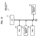
- FIG. 12 illustrates an exemplary control section that operates in accordance with the conventional accessing manner.
- a main control section 21 of a digital copier is controlled by a CPU 211, and includes a ROM 212, a working memory 213, a timer 214, and a non-volatile memory 215, respectively connected to each other via a CPU bus.
- the CPU 211 of the main control section 21 performs a series of control operations in accordance with control program stored in the ROM 212 after the electrical power is supplied (ON).
- the working memory 213 is utilized as a working area, and the non-volatile memory 215 is utilized so as to store a variety of important information to be preserved together with the above-described usage information.
- the timer 214 is provided so as to generate a timing signal for periodically updating the non-volatile memory 215.
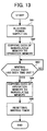
- Fig. 13 illustrates a conventional operation control flow for reading and writing data from and to a non-volatile memory in the system of Fig. 12.
- the electrical power is initially supplied, and data of the non-volatile memory 215 is simultaneously copied to the working memory 213 (S62).
- reference and update operations are performed (not shown in the flow) with regard to the working memory 213 so as to change usage information stored therein in accordance with a change in usage information when an image forming apparatus is operated.
- the non-volatile memory 215 is not accessed.
- the timer 214 times and determines a preset writing cycle (S63), and data of the working memory 213 is copied to the non-volatile memory 215 every timeout (S64). Then, the timer 214 is reset (S65), and the flow is terminated.
- Such a writing cycle of the timer 214 is generally optionally set.
- the writing cycle is preferably set in view of a rewritable lifetime of the non-volatile memory 215, the lifetime can meets with a product lifetime of the image forming apparatus.
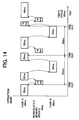
- Fig. 14 illustrates a usage condition of such a conventional system that updates information stored in the non-volatile memory at a cycle set by the timer. As shown in Fig.
- update duration of 10 milliseconds for updating the non-volatile memory 215 periodically occupies the CPU bus in a timeout cycle of 80ms, and accordingly, performing a task A (50ms) three times and a task B (30ms) twice takes in total 240ms.
- an object of the present invention is to address and resolve the above and other problems and to provide a new image forming apparatus.
- a novel image forming apparatus including a volatile memory configured to temporarily store usage information of the image forming apparatus, and a non-volatile memory configured to finally or permanently store the usage information.
- An access control device may be provided so as to access and output at least address, data, and a variety of control signals to the non-volatile memory as private usage signals different from outputs of the CPU.
- the access control device may copy the usage information stored in the non-volatile memory to the volatile memory, and update the non-volatile memory with information newly stored in the volatile memory.
- an updating device may be provided so as to periodically update usage information stored in the non-volatile memory at a prescribed timing.
- an access cycle changing device may be provided so as to change a number of cycles for accessing to the non-volatile memory based upon setting.
- a switching device may be provided so as to switch an accessing manner for accessing to the non-volatile memory from normal read and write to burst read and write vice versa in accordance with setting.
- the access control device is made into an IC, and one of the access cycle changing device and the access manner switching device is built in the IC.
- the volatile memory includes any one of an SRAM and a DRAM built in the IC.
- the non-volatile memory includes any one of an EEPROM and a ferroelectric substance memory.
- a digital copier is illustrated as one preferred example of an image forming apparatus according to the present invention.
- the digital copier 11 may include a reading control section 111 for reading an original document 12, an operation section 112 for functioning as a user interface, and a power supply 116.
- the digital copier 11 may also include a main control section 113 for controlling all of the reading control section 111, the operation section 112, and the power supply 116, and process read image data.
- a writing control section 114 for receiving image data from the main control section 113, and an electro-photographic process section 115 for forming, i.e., an image, and a copy in accordance with an output from the writing control section 114 may be provided.
- image data may be read by the reading control section 111 and may experience additional processing such as A/D conversion, correction, etc.
- the image data may further experience image processing from an image processing section (not shown) provided in the main control section 113 to be converted into image formation usage data, and is then transmitted to the writing control section 114.
- the writing control section 114 may control a laser diode (not shown) for optical writing based upon the image data transmitted from the image processing section.
- the writing control section 114 may form an electrostatic latent image on a photoconductive member provided in the electro-photographic process section 115 using a laser beam emitted from the laser diode. Subsequently, a known electro-photographic process may be performed so as to form a copy 13.
- Fig. 2 illustrates the main hardware components of the main control section of Fig. 1.
- the main control section 51 may include an ASIC (application-specific integrated circuit) 516 controlled by a CPU 511, a ROM 512, a working memory 513, a timer 514, and a data memory 517 each connected to the CPU 511 via a CPU bus.
- the CPU 511 may operate in order to control the reading control section 111, the operation section 112, and the power supply 116 in accordance with a control program stored in the ROM 512.
- the CPU 511 may also operate in order to control the entire image forming apparatus. Data and information such as the control program used for operating the CPU 511 may be stored in the ROM 512.
- Information necessary for a control operation or information generated during image formation as history (career) data may also be stored in the non-volatile memory 515.
- a non-volatile memory storing usage information that may change in accordance with usage condition is directly connected to a CPU via a CPU bus in a manner similar to a ROM or a working memory.
- such a non-volatile memory is accessed so as to update the usage information under direct control of the CPU. Accordingly, conventionally the performance is lowered as described earlier.
- a prescribed device may be provided so as to shorten a period of time when the CPU 511 drives to update usage information of the non-volatile memory as much as possible and to reduce the burden or computing load of the CPU 511. As a result, the performance of the entire system may be not lowered.
- the ASIC 516 may disable the CPU 511 to directly access the non-volatile memory 515 as illustrated in Fig. 2.
- the non-volatile memory 515 may be enabled to communicate a private usage control signal with an access control device (not shown) provided in the ASIC 516, and is controlled by the CPU 511 via the ASIC 516.
- a control operation performed by the CPU 511 is now briefly described. After the electric power is supplied, the CPU 511 may perform a series of control operations in accordance with a control program stored in the ROM 512. The working memory 513 may then function as a working area for the CPU 511. By connecting the non-volatile memory 515 to the CPU 511 with a non-volatile memory private usage control signal generated by the ASIC 516, the non-volatile memory 515 can not be accessed in synchronism with a control signal of the CPU 511. In addition, the data memory 517 may receive the non-volatile memory private usage control signal.
- a copying operation (when the electric power is supplied) and periodical updating of the non-volatile memory 515 may be performed between the non-volatile memory 515 and the data memory 517.
- those operations may not be performed directly to the non-volatile memory 515 but may be mediated instead.
- the cycle of updating the non-volatile memory 515 may be adjusted by the timer 514 so that such an updating operation is repeated every time when a prescribed time period has elapsed. Further, such a timer 514 can be integrated in the ASIC 516.
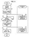
- Fig. 3 illustrates an exemplary control flow of a data updating process performed with regard to the non-volatile memory 515 of Fig. 2.
- the electric power may be supplied (S31).
- the CPU 511 may issue a recall command and enable the ASIC 516 to copy data of the non-volatile memory 515 to the data memory 517 of the ASIC 516 (S32).
- the ASIC 516 may receive and execute the recall command, i.e., copy the data of the non-volatile memory 515 to the data memory 517 (S33), and inform the CPU 511 of termination of the copying process.
- ordinarily performed reference and update operations (not shown) with regard to a variety of usage information, which are performed based upon an operation of the digital copier 11 controlled by the CPU 511, may be directed to the data memory 517. Specifically, the ordinarily performed reference and update operations may not be directed to the non-volatile memory 515.
- the data of the data memory 517 may be copied to the non-volatile memory 515.
- a timeout time may optionally be set to the timer 514 so as to generate the timeout signal. If such a timeout time is set in view of the rewriting lifetime of the non-volatile memory 515, the lifetime of the non-volatile memory 515 can substantially meet with the lifetime of the product.
- the CPU 511 may initially issue a command instructing that data of the data memory 517 is copied to the non-volatile memory 515.
- the CPU 511 may then check the timeout of the timer 514 (S34), and issue a store command to the ASIC 516, instructing that data of the data memory 517 should be copied to the non-volatile memory 515, if the timeout is confirmed (S35).
- the ASIC 516 may receive and execute the store command and copy the data of the data memory 517 to the non-volatile memory 515 (S36), and inform the CPU 511 of the termination thereof.
- the CPU 511 may receive the termination information, and reset the writing timer 514 in order to set the next timeout (S37). Then, the flow may be terminated.
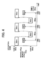
- Fig. 4 illustrates such a usage condition of the CPU bus, wherein an update is independently performed from an operation of the CPU 511. Since an update of the non-volatile memory 515 for 10ms does not occupy the CPU bus, three times of the task A taking 50ms and twice of the task B taking 30ms may be terminated within 210ms. It may be realized that the same tasks can be terminated earlier by 30ms than the conventional example illustrated in Fig. 14.
- an SRAM can be employed as a data memory 517 integrated in the ASIC 516 to simplify the configuration of a control circuit, because it need not to be controlled. Specifically, refreshing and hardwiring to an external device may be not needed due to its installation in the ASIC 516.
- a DRAM can also be employed as a data memory 517. Since the DRAM offers a higher storage capacity in substantially the same cell area as compared to the SRAM, the DRAM may readily handle a non-volatile memory having a high capacity. In addition, since hardwiring to the outside is needless due to its installation in the ASIC 516, configuration of a control circuit can be simplified.
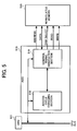
- FIG. 5 illustrates still another modification of the main control section illustrated in Fig. 2.
- the ASIC 516 may include and connect a control signal generation section 519 serving as an access control device and accessing the non-volatile memory 515 and an access cycle changing section 518 to a CPU 511 via the CPU bus.
- the control signal generation section 519 may generate address, data, chip select, and read and write signals as private usage control signals transmitted to the non-volatile memory 515.
- the control signal generation section 519 may control the data memory 517 to transmit and receive data to and from the non-volatile memory 515.
- the access cycle changing section 518 may be enabled to optionally change a cycle of an access to the non-volatile memory 515 based upon an instruction from the CPU 511.
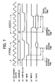
- Figs. 6 and 7 are time charts for illustrating control signals and various data operations performed when the access cycle changing section 518 changes an access cycle.
- the control signal generation section 519 may generate a reference clock as illustrated in the respective drawings.
- Fig. 6 illustrates a case when an access is performed to the non-volatile memory 515 in three cycles of reference clocks, namely, the control signal generation section 519 generates respective control signals so that the access can be completed during a time period corresponding to three cycles.
- Fig. 6 illustrates a relation between the timing generation of a control signal and an accessing time period for accessing to a device when both reading and writing are performed.
- Fig. 7 illustrates a case when a cycle of the access is four cycles. As becomes apparent from a comparison of Fig.
- a read access time, an address access time, a write set up time, and an address set up time required when reading and writing are performed in the four cycles may be longer than respective of those when performed in the three cycles.
- an access time may be adjusted in accordance with a number of access cycles. Accordingly, a memory having a slower access time can be handled.
- Such burst reading and writing may enable the ASIC 516 to successively read and write data from and to a plurality of addresses of the non-volatile memory.
- this embodiment may propose to readily handle various types of non-volatile memories working in various ways by preferably selecting one of normal and burst reading and writing manners when accessing to a non-volatile memory in accordance with a changeably set cycle.
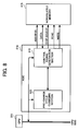
- Fig. 8 briefly illustrates a main control section of this embodiment.
- the ASIC 516 may include and connect a control signal generation section 519 serving as an access control device and accessing to the non-volatile memory 515 and a pre-charge cycle changing section 520 to a CPU 511 via a CPU bus.
- the control signal generation section 519 may generate address, data, chip select, and read and write signals as private usage control signals so as to control data transmission performed between the data memory 517 and the non-volatile memory 515.
- a pre-charge cycle changing section 520 capable of optionally selecting insertion of a pre-charge cycle may select a pre-charge cycle. Such selection may be performed based upon an instruction from the CPU 511.
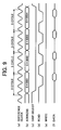
- Figs. 9 and 10 illustrate time charts for illustrating operations performed when the pre-charge cycle is inserted or omitted, and the burst read or normal read is set through the pre-charge cycle changing section 520.
- a reference clock illustrated in these drawings may be generated by the control signal generating section 519 of Fig. 8.
- Fig. 9 illustrates an access cycle when a burst read is performed from a non-volatile memory. Since the pre-charge process is not inserted, data can be read from different addresses at a high speed only by changing an address while maintaining a chip select signal active.
- Fig. 10 illustrates another access cycle when a normal read is performed. As noted from Fig.
- a pre-charge time period may be required and the normal read is performed in prescribed cycles in which one cycle of a pre-charge time period is added to three cycles of an access time period. As a result, data reading may be delayed by the pre-charge time period.
- Fig. 11 briefly illustrates a main control section of this example.
- the ASIC 516 may include and connect a control signal generation section 519 serving as an access control device and accessing to the non-volatile memory 515, an access cycle changing section 518, and a pre-charge cycle changing section 520 to a CPU 511 via a CPU bus.
- the control signal generation section 519 again generates address, data, chip select, and read and write signals as private usage signals transmitted to the non-volatile memory 515.
- control signal generation section 519 may control data transmission performed between the data memory 517 and the non-volatile memory 515. All of the control signal generation section 519, the access cycle changing section 518, and the pre-charge cycle changing section 520 may operate in a manner similar to that described earlier.
- the above-described selecting device can be integrated into an integrated circuit and operated with its scale and number of parts being suppressed to the least levels, respectively.
- an EEPROM can be employed at least in a portion of the non-volatile memory. Because, the EEPROM is employable in various ways due to its large variations and cheapness.
- a ferroelectric substance memory can also be employed in a similar manner. Because, the ferroelectric substance memory may have a longer rewritable life and a larger capacity than the EEPROM. Owing to these characteristics, the likelihood of data updating errors whose possibility generally increases in proportion to the frequency of power supply stoppage and of accidents or failures may be decreased.
- the mechanisms and processes set forth in the present invention may be implemented using one or more conventional general purpose microprocessors and/or signal processors programmed according to the teachings in the present specification as will be appreciated by those skilled in the relevant arts.
- Appropriate software coding can readily be prepared by skilled programmers based on the teachings of the present disclosure, as will also be apparent to those skilled in the relevant arts.
- the present invention also may be implemented by the preparation of application-specific integrated circuits (ASICS) by interconnecting an appropriate network of conventional component circuits or by a combination thereof with one or more conventional general purpose microprocessors and/or signal processors programmed accordingly.
- ASICS application-specific integrated circuits
- the present invention thus also includes a computer-based product or computer program which may be hosted on a storage medium and include, but is not limited to, any type of disk including floppy disks, optical disks, CD-ROMs, magnet-optical disks, ROMs, RAMs, EPROMs, EEPROMs, flash memory, magnetic or optical cards, or any type of media suitable for storing electronic instructions or computer program code portions.
- a computer-based product or computer program which may be hosted on a storage medium and include, but is not limited to, any type of disk including floppy disks, optical disks, CD-ROMs, magnet-optical disks, ROMs, RAMs, EPROMs, EEPROMs, flash memory, magnetic or optical cards, or any type of media suitable for storing electronic instructions or computer program code portions.
Landscapes
- Engineering & Computer Science (AREA)
- Multimedia (AREA)
- Signal Processing (AREA)
- Health & Medical Sciences (AREA)
- Biomedical Technology (AREA)
- General Health & Medical Sciences (AREA)
- Physics & Mathematics (AREA)
- General Physics & Mathematics (AREA)
- Techniques For Improving Reliability Of Storages (AREA)
- Memory System (AREA)
- Facsimiles In General (AREA)
- Accessory Devices And Overall Control Thereof (AREA)
- Record Information Processing For Printing (AREA)
Applications Claiming Priority (4)
| Application Number | Priority Date | Filing Date | Title |
|---|---|---|---|
| JP2001074365 | 2001-03-15 | ||
| JP2001074365 | 2001-03-15 | ||
| JP2001221816 | 2001-07-23 | ||
| JP2001221816A JP2002337402A (ja) | 2001-03-15 | 2001-07-23 | 画像形成装置 |
Publications (2)
| Publication Number | Publication Date |
|---|---|
| EP1244285A1 true EP1244285A1 (fr) | 2002-09-25 |
| EP1244285B1 EP1244285B1 (fr) | 2006-05-10 |
Family
ID=26611344
Family Applications (1)
| Application Number | Title | Priority Date | Filing Date |
|---|---|---|---|
| EP02005390A Expired - Lifetime EP1244285B1 (fr) | 2001-03-15 | 2002-03-15 | Circuit pour prolonger la vie des mémoires non volatiles et appareil de formation d'images |
Country Status (4)
| Country | Link |
|---|---|
| US (1) | US7221468B2 (fr) |
| EP (1) | EP1244285B1 (fr) |
| JP (1) | JP2002337402A (fr) |
| DE (1) | DE60211239T2 (fr) |
Families Citing this family (12)
| Publication number | Priority date | Publication date | Assignee | Title |
|---|---|---|---|---|
| US7133926B2 (en) * | 2001-09-28 | 2006-11-07 | Hewlett-Packard Development Company, L.P. | Broadcast compressed firmware flashing |
| US7251711B2 (en) | 2002-05-28 | 2007-07-31 | Micron Technology, Inc. | Apparatus and methods having a command sequence |
| JP3765806B2 (ja) * | 2002-07-22 | 2006-04-12 | 三星電子株式会社 | 画像形成装置 |
| TW200702891A (en) * | 2005-07-15 | 2007-01-16 | Coretronic Corp | Projector, and a control method of the bulb brightness for the projector |
| US20070024764A1 (en) * | 2005-07-29 | 2007-02-01 | Optoma Technology, Inc. | Methods and systems that compensate for distortion introduced by anamorphic lenses in a video projector |
| JP5171448B2 (ja) * | 2007-07-31 | 2013-03-27 | キヤノン株式会社 | 画像形成装置及びその制御方法 |
| JP2009181337A (ja) * | 2008-01-30 | 2009-08-13 | Ricoh Co Ltd | 画像形成システム、管理装置、画像形成装置、画像形成方法、及び画像形成プログラム |
| JP2009193163A (ja) * | 2008-02-12 | 2009-08-27 | Ricoh Co Ltd | 画像形成システム、管理装置、通信制御装置、画像形成方法、及び画像形成プログラム |
| JP5332226B2 (ja) * | 2008-02-20 | 2013-11-06 | 横河電機株式会社 | 可動部品稼動情報の保持方法とこれを用いた機器 |
| JP6270377B2 (ja) * | 2013-08-27 | 2018-01-31 | キヤノン株式会社 | 画像形成装置 |
| CN103501398B (zh) * | 2013-09-24 | 2016-08-31 | 珠海艾派克微电子有限公司 | 芯片、成像盒及芯片与成像设备的通讯方法 |
| CN103879152B (zh) * | 2014-03-07 | 2015-10-14 | 珠海艾派克微电子有限公司 | 用于存储成像盒信息的盒芯片、成像盒及通信方法 |
Citations (7)
| Publication number | Priority date | Publication date | Assignee | Title |
|---|---|---|---|---|
| GB2244582A (en) * | 1990-05-04 | 1991-12-04 | British Telecomm | Vehicle usage monitor system |
| EP0566264A1 (fr) * | 1992-04-16 | 1993-10-20 | International Business Machines Corporation | Ordinateur à piles avec jaugeur de niveau de la pile et méthode pour mesurer l'état de charge d'une pile |
| EP0859489A2 (fr) * | 1997-02-14 | 1998-08-19 | Toshiba America Information Systems, Inc. | Système de surveillance à distance |
| US5835816A (en) * | 1995-01-19 | 1998-11-10 | Ricoh Company, Ltd. | Remote service system for image forming apparatuses |
| EP0905963A2 (fr) * | 1997-09-26 | 1999-03-31 | Ricoh Company, Ltd. | Appareil et procédé pour la transmission de données de mesure de la performance vers un centre de contrÔle |
| EP0946046A2 (fr) * | 1998-03-27 | 1999-09-29 | Canon Kabushiki Kaisha | Dispositif de traitement d'image, procédé de commande d'un dispositif de traitement d'image, et support d'enregistrement pour l'enregistrement d'un programme de commande pour un dispositif de traitement d'image |
| EP1043885A2 (fr) * | 1999-04-09 | 2000-10-11 | Canon Kabushiki Kaisha | Procédé de négociation d'échange des fonctions de traitement d'images |
Family Cites Families (14)
| Publication number | Priority date | Publication date | Assignee | Title |
|---|---|---|---|---|
| US4901273A (en) * | 1985-03-12 | 1990-02-13 | Pitney Bowes Inc. | Electronic postage meter having a memory map decoder |
| JPH05270055A (ja) * | 1992-03-30 | 1993-10-19 | Canon Inc | 画像記録方法及び装置及び情報処理方法 |
| JPH06312561A (ja) * | 1993-04-30 | 1994-11-08 | Tokyo Electric Co Ltd | プリンタ |
| JPH08161134A (ja) * | 1994-12-05 | 1996-06-21 | Canon Inc | 印刷装置及びそのメンテナンス方法 |
| JPH0950431A (ja) * | 1995-08-08 | 1997-02-18 | Canon Inc | フォントデータの管理方法及びこれを適用するシステム,装置 |
| JPH11147322A (ja) * | 1997-08-29 | 1999-06-02 | Seiko Epson Corp | プリンタ |
| JPH11170675A (ja) * | 1997-12-11 | 1999-06-29 | Ricoh Co Ltd | プリンタシステム |
| JPH11275298A (ja) * | 1998-01-19 | 1999-10-08 | Brother Ind Ltd | ファクシミリ送信システム |
| JP3969891B2 (ja) * | 1998-04-16 | 2007-09-05 | キヤノン株式会社 | 画像形成装置 |
| JP4060442B2 (ja) * | 1998-05-28 | 2008-03-12 | 富士通株式会社 | メモリデバイス |
| JP2000141808A (ja) * | 1998-11-09 | 2000-05-23 | Seiko Epson Corp | プリンタ及びプリンタ用モータの制御装置 |
| JP3758867B2 (ja) * | 1998-12-03 | 2006-03-22 | セイコーエプソン株式会社 | 画像形成装置用寿命管理装置 |
| JP3519017B2 (ja) * | 1999-04-02 | 2004-04-12 | シャープ株式会社 | 画像形成装置 |
| JP2000299767A (ja) * | 1999-04-14 | 2000-10-24 | Oki Data Corp | スキャナ付きプリンタ |
-
2001
- 2001-07-23 JP JP2001221816A patent/JP2002337402A/ja active Pending
-
2002
- 2002-03-14 US US10/096,818 patent/US7221468B2/en not_active Expired - Fee Related
- 2002-03-15 EP EP02005390A patent/EP1244285B1/fr not_active Expired - Lifetime
- 2002-03-15 DE DE60211239T patent/DE60211239T2/de not_active Expired - Lifetime
Patent Citations (7)
| Publication number | Priority date | Publication date | Assignee | Title |
|---|---|---|---|---|
| GB2244582A (en) * | 1990-05-04 | 1991-12-04 | British Telecomm | Vehicle usage monitor system |
| EP0566264A1 (fr) * | 1992-04-16 | 1993-10-20 | International Business Machines Corporation | Ordinateur à piles avec jaugeur de niveau de la pile et méthode pour mesurer l'état de charge d'une pile |
| US5835816A (en) * | 1995-01-19 | 1998-11-10 | Ricoh Company, Ltd. | Remote service system for image forming apparatuses |
| EP0859489A2 (fr) * | 1997-02-14 | 1998-08-19 | Toshiba America Information Systems, Inc. | Système de surveillance à distance |
| EP0905963A2 (fr) * | 1997-09-26 | 1999-03-31 | Ricoh Company, Ltd. | Appareil et procédé pour la transmission de données de mesure de la performance vers un centre de contrÔle |
| EP0946046A2 (fr) * | 1998-03-27 | 1999-09-29 | Canon Kabushiki Kaisha | Dispositif de traitement d'image, procédé de commande d'un dispositif de traitement d'image, et support d'enregistrement pour l'enregistrement d'un programme de commande pour un dispositif de traitement d'image |
| EP1043885A2 (fr) * | 1999-04-09 | 2000-10-11 | Canon Kabushiki Kaisha | Procédé de négociation d'échange des fonctions de traitement d'images |
Also Published As
| Publication number | Publication date |
|---|---|
| US20020131085A1 (en) | 2002-09-19 |
| EP1244285B1 (fr) | 2006-05-10 |
| JP2002337402A (ja) | 2002-11-27 |
| DE60211239D1 (de) | 2006-06-14 |
| US7221468B2 (en) | 2007-05-22 |
| DE60211239T2 (de) | 2007-03-01 |
Similar Documents
| Publication | Publication Date | Title |
|---|---|---|
| US5673383A (en) | Storage system with a flash memory module | |
| KR100408872B1 (ko) | 플래시 마이크로컴퓨터의 프로그램 재기록 방법 | |
| EP1244285B1 (fr) | Circuit pour prolonger la vie des mémoires non volatiles et appareil de formation d'images | |
| US9819820B2 (en) | Chip, imaging cartridge, and communication method between the chip and imaging device | |
| US8051270B2 (en) | Memory controller, nonvolatile storage device, nonvolatile storage system, and memory control method | |
| JP6146675B2 (ja) | 画像形成装置及びフラッシュメモリの制御方法並びに制御プログラム | |
| JPH04261566A (ja) | ディジタル画像出力装置 | |
| JP4848330B2 (ja) | 画像形成装置、画像形成方法、およびプログラム | |
| WO2007015722A2 (fr) | Adressage, protocole de commande, et interface electrique pour memoires non volatiles utilisees pour enregistrer des comptabilisations d'utilisation | |
| JP6308433B2 (ja) | 画像形成装置及び制御方法並びに制御プログラム | |
| JP3677012B2 (ja) | 携帯用コンピュータのキーボード−コマンド読み取り装置 | |
| US7680980B2 (en) | Image forming apparatus | |
| US6792223B2 (en) | Image forming apparatus for reducing a system return time | |
| US20080094662A1 (en) | Image forming apparatus | |
| JPH0512137A (ja) | 情報処理装置 | |
| JP2001356967A (ja) | 不揮発性メモリの書込制御方法 | |
| JP4041052B2 (ja) | 画像形成装置 | |
| JPH11133683A (ja) | 画像形成装置 | |
| JP2019185597A (ja) | メモリ制御装置、メモリ装置、画像形成装置、及びプログラム | |
| JP2019020846A (ja) | 情報処理装置及びその制御方法、並びにプログラム | |
| JPH07299945A (ja) | 印字装置 | |
| JP2006279539A (ja) | 画像記憶装置および画像記憶方法 | |
| US7161703B2 (en) | Image processing system having a storage section being accessed directly | |
| KR100389760B1 (ko) | 아이피씨용 에프아이에프오의 번지 관리 시스템 및 방법 | |
| JP2008134558A (ja) | 画像形成装置およびその調整値設定方法 |
Legal Events
| Date | Code | Title | Description |
|---|---|---|---|
| PUAI | Public reference made under article 153(3) epc to a published international application that has entered the european phase |
Free format text: ORIGINAL CODE: 0009012 |
|
| AK | Designated contracting states |
Kind code of ref document: A1 Designated state(s): AT BE CH CY DE DK ES FI FR GB GR IE IT LI LU MC NL PT SE TR |
|
| AX | Request for extension of the european patent |
Free format text: AL;LT;LV;MK;RO;SI |
|
| 17P | Request for examination filed |
Effective date: 20021105 |
|
| AKX | Designation fees paid |
Designated state(s): DE FR GB |
|
| 17Q | First examination report despatched |
Effective date: 20030917 |
|
| GRAP | Despatch of communication of intention to grant a patent |
Free format text: ORIGINAL CODE: EPIDOSNIGR1 |
|
| GRAS | Grant fee paid |
Free format text: ORIGINAL CODE: EPIDOSNIGR3 |
|
| GRAA | (expected) grant |
Free format text: ORIGINAL CODE: 0009210 |
|
| AK | Designated contracting states |
Kind code of ref document: B1 Designated state(s): DE FR GB |
|
| REG | Reference to a national code |
Ref country code: GB Ref legal event code: FG4D |
|
| REF | Corresponds to: |
Ref document number: 60211239 Country of ref document: DE Date of ref document: 20060614 Kind code of ref document: P |
|
| ET | Fr: translation filed | ||
| PLBE | No opposition filed within time limit |
Free format text: ORIGINAL CODE: 0009261 |
|
| STAA | Information on the status of an ep patent application or granted ep patent |
Free format text: STATUS: NO OPPOSITION FILED WITHIN TIME LIMIT |
|
| 26N | No opposition filed |
Effective date: 20070213 |
|
| REG | Reference to a national code |
Ref country code: FR Ref legal event code: PLFP Year of fee payment: 15 |
|
| PGFP | Annual fee paid to national office [announced via postgrant information from national office to epo] |
Ref country code: FR Payment date: 20160321 Year of fee payment: 15 Ref country code: GB Payment date: 20160321 Year of fee payment: 15 |
|
| PGFP | Annual fee paid to national office [announced via postgrant information from national office to epo] |
Ref country code: DE Payment date: 20160330 Year of fee payment: 15 |
|
| REG | Reference to a national code |
Ref country code: DE Ref legal event code: R119 Ref document number: 60211239 Country of ref document: DE |
|
| GBPC | Gb: european patent ceased through non-payment of renewal fee |
Effective date: 20170315 |
|
| REG | Reference to a national code |
Ref country code: FR Ref legal event code: ST Effective date: 20171130 |
|
| PG25 | Lapsed in a contracting state [announced via postgrant information from national office to epo] |
Ref country code: DE Free format text: LAPSE BECAUSE OF NON-PAYMENT OF DUE FEES Effective date: 20171003 Ref country code: FR Free format text: LAPSE BECAUSE OF NON-PAYMENT OF DUE FEES Effective date: 20170331 |
|
| PG25 | Lapsed in a contracting state [announced via postgrant information from national office to epo] |
Ref country code: GB Free format text: LAPSE BECAUSE OF NON-PAYMENT OF DUE FEES Effective date: 20170315 |