EP1298698A1 - Procédé et appareil d'ajustement de caractéristiques d'un dispositif de formation d'images et procédé de fabrication d'un dispositif de formation d'images - Google Patents
Procédé et appareil d'ajustement de caractéristiques d'un dispositif de formation d'images et procédé de fabrication d'un dispositif de formation d'images Download PDFInfo
- Publication number
- EP1298698A1 EP1298698A1 EP02021675A EP02021675A EP1298698A1 EP 1298698 A1 EP1298698 A1 EP 1298698A1 EP 02021675 A EP02021675 A EP 02021675A EP 02021675 A EP02021675 A EP 02021675A EP 1298698 A1 EP1298698 A1 EP 1298698A1
- Authority
- EP
- European Patent Office
- Prior art keywords
- electron
- emitting devices
- luminance
- emitting
- characteristic
- Prior art date
- Legal status (The legal status is an assumption and is not a legal conclusion. Google has not performed a legal analysis and makes no representation as to the accuracy of the status listed.)
- Granted
Links
- 238000000034 method Methods 0.000 title claims abstract description 90
- 238000004519 manufacturing process Methods 0.000 title claims description 20
- 238000005259 measurement Methods 0.000 claims abstract description 65
- 239000000758 substrate Substances 0.000 claims abstract description 29
- 238000010894 electron beam technology Methods 0.000 claims abstract description 24
- 230000001360 synchronised effect Effects 0.000 claims description 10
- 239000012789 electroconductive film Substances 0.000 claims description 6
- 230000003213 activating effect Effects 0.000 claims description 3
- 238000004364 calculation method Methods 0.000 claims description 2
- 239000002772 conduction electron Substances 0.000 description 56
- 238000012545 processing Methods 0.000 description 33
- 230000008569 process Effects 0.000 description 25
- 239000011159 matrix material Substances 0.000 description 22
- 239000010408 film Substances 0.000 description 14
- 230000003287 optical effect Effects 0.000 description 14
- 230000008859 change Effects 0.000 description 10
- 239000010409 thin film Substances 0.000 description 8
- OAICVXFJPJFONN-UHFFFAOYSA-N Phosphorus Chemical compound [P] OAICVXFJPJFONN-UHFFFAOYSA-N 0.000 description 7
- 238000001994 activation Methods 0.000 description 7
- 230000001133 acceleration Effects 0.000 description 6
- 230000004913 activation Effects 0.000 description 6
- 239000000463 material Substances 0.000 description 6
- 239000002184 metal Substances 0.000 description 6
- OKTJSMMVPCPJKN-UHFFFAOYSA-N Carbon Chemical compound [C] OKTJSMMVPCPJKN-UHFFFAOYSA-N 0.000 description 5
- 239000012298 atmosphere Substances 0.000 description 5
- 230000005684 electric field Effects 0.000 description 5
- 239000005416 organic matter Substances 0.000 description 5
- 230000007423 decrease Effects 0.000 description 4
- 238000010586 diagram Methods 0.000 description 4
- XOLBLPGZBRYERU-UHFFFAOYSA-N tin dioxide Chemical compound O=[Sn]=O XOLBLPGZBRYERU-UHFFFAOYSA-N 0.000 description 4
- 239000003086 colorant Substances 0.000 description 3
- 239000004020 conductor Substances 0.000 description 3
- 238000013500 data storage Methods 0.000 description 3
- 229910002804 graphite Inorganic materials 0.000 description 3
- 239000010439 graphite Substances 0.000 description 3
- 230000009471 action Effects 0.000 description 2
- 229910052799 carbon Inorganic materials 0.000 description 2
- 238000010438 heat treatment Methods 0.000 description 2
- 238000005304 joining Methods 0.000 description 2
- 238000007789 sealing Methods 0.000 description 2
- 230000006641 stabilisation Effects 0.000 description 2
- 238000011105 stabilization Methods 0.000 description 2
- 229910003481 amorphous carbon Inorganic materials 0.000 description 1
- 230000008901 benefit Effects 0.000 description 1
- 150000001722 carbon compounds Chemical class 0.000 description 1
- 239000011248 coating agent Substances 0.000 description 1
- 238000000576 coating method Methods 0.000 description 1
- 230000003247 decreasing effect Effects 0.000 description 1
- 238000000151 deposition Methods 0.000 description 1
- 238000013461 design Methods 0.000 description 1
- 238000009826 distribution Methods 0.000 description 1
- 230000000694 effects Effects 0.000 description 1
- 238000001704 evaporation Methods 0.000 description 1
- 238000002474 experimental method Methods 0.000 description 1
- 239000007789 gas Substances 0.000 description 1
- 239000011521 glass Substances 0.000 description 1
- 238000009499 grossing Methods 0.000 description 1
- PJXISJQVUVHSOJ-UHFFFAOYSA-N indium(III) oxide Inorganic materials [O-2].[O-2].[O-2].[In+3].[In+3] PJXISJQVUVHSOJ-UHFFFAOYSA-N 0.000 description 1
- 238000009413 insulation Methods 0.000 description 1
- 239000012212 insulator Substances 0.000 description 1
- 230000001788 irregular Effects 0.000 description 1
- 230000007774 longterm Effects 0.000 description 1
- 238000007726 management method Methods 0.000 description 1
- 229910044991 metal oxide Inorganic materials 0.000 description 1
- 150000004706 metal oxides Chemical class 0.000 description 1
- 239000000203 mixture Substances 0.000 description 1
- 239000012299 nitrogen atmosphere Substances 0.000 description 1
- NJPPVKZQTLUDBO-UHFFFAOYSA-N novaluron Chemical compound C1=C(Cl)C(OC(F)(F)C(OC(F)(F)F)F)=CC=C1NC(=O)NC(=O)C1=C(F)C=CC=C1F NJPPVKZQTLUDBO-UHFFFAOYSA-N 0.000 description 1
- 230000009467 reduction Effects 0.000 description 1
- 230000004044 response Effects 0.000 description 1
- 238000009827 uniform distribution Methods 0.000 description 1
- 238000007738 vacuum evaporation Methods 0.000 description 1
Images




Classifications
-
- H—ELECTRICITY
- H01—ELECTRIC ELEMENTS
- H01J—ELECTRIC DISCHARGE TUBES OR DISCHARGE LAMPS
- H01J9/00—Apparatus or processes specially adapted for the manufacture, installation, removal, maintenance of electric discharge tubes, discharge lamps, or parts thereof; Recovery of material from discharge tubes or lamps
- H01J9/44—Factory adjustment of completed discharge tubes or lamps to comply with desired tolerances
-
- G—PHYSICS
- G09—EDUCATION; CRYPTOGRAPHY; DISPLAY; ADVERTISING; SEALS
- G09G—ARRANGEMENTS OR CIRCUITS FOR CONTROL OF INDICATING DEVICES USING STATIC MEANS TO PRESENT VARIABLE INFORMATION
- G09G3/00—Control arrangements or circuits, of interest only in connection with visual indicators other than cathode-ray tubes
- G09G3/006—Electronic inspection or testing of displays and display drivers, e.g. of LED or LCD displays
-
- G—PHYSICS
- G09—EDUCATION; CRYPTOGRAPHY; DISPLAY; ADVERTISING; SEALS
- G09G—ARRANGEMENTS OR CIRCUITS FOR CONTROL OF INDICATING DEVICES USING STATIC MEANS TO PRESENT VARIABLE INFORMATION
- G09G3/00—Control arrangements or circuits, of interest only in connection with visual indicators other than cathode-ray tubes
- G09G3/20—Control arrangements or circuits, of interest only in connection with visual indicators other than cathode-ray tubes for presentation of an assembly of a number of characters, e.g. a page, by composing the assembly by combination of individual elements arranged in a matrix no fixed position being assigned to or needed to be assigned to the individual characters or partial characters
- G09G3/22—Control arrangements or circuits, of interest only in connection with visual indicators other than cathode-ray tubes for presentation of an assembly of a number of characters, e.g. a page, by composing the assembly by combination of individual elements arranged in a matrix no fixed position being assigned to or needed to be assigned to the individual characters or partial characters using controlled light sources
-
- H—ELECTRICITY
- H01—ELECTRIC ELEMENTS
- H01J—ELECTRIC DISCHARGE TUBES OR DISCHARGE LAMPS
- H01J31/00—Cathode ray tubes; Electron beam tubes
- H01J31/08—Cathode ray tubes; Electron beam tubes having a screen on or from which an image or pattern is formed, picked up, converted, or stored
- H01J31/10—Image or pattern display tubes, i.e. having electrical input and optical output; Flying-spot tubes for scanning purposes
- H01J31/12—Image or pattern display tubes, i.e. having electrical input and optical output; Flying-spot tubes for scanning purposes with luminescent screen
- H01J31/123—Flat display tubes
- H01J31/125—Flat display tubes provided with control means permitting the electron beam to reach selected parts of the screen, e.g. digital selection
- H01J31/127—Flat display tubes provided with control means permitting the electron beam to reach selected parts of the screen, e.g. digital selection using large area or array sources, i.e. essentially a source for each pixel group
-
- G—PHYSICS
- G09—EDUCATION; CRYPTOGRAPHY; DISPLAY; ADVERTISING; SEALS
- G09G—ARRANGEMENTS OR CIRCUITS FOR CONTROL OF INDICATING DEVICES USING STATIC MEANS TO PRESENT VARIABLE INFORMATION
- G09G2320/00—Control of display operating conditions
- G09G2320/02—Improving the quality of display appearance
- G09G2320/0285—Improving the quality of display appearance using tables for spatial correction of display data
Definitions
- the present invention relates to an image forming apparatus provided with a large number of surface conduction electron emission devices and to a characteristics adjustment method for an image forming apparatus, a manufacturing method for an image forming apparatus and a characteristics adjustment apparatus that are preferably applied to such an image forming apparatus.
- a hot cathode device for example, a field emission device.
- a metal/insulator/metal electron-emitting device and a surface conduction electron emission device are known.
- the surface conduction electron emission device (hereinafter also referred to simply as device) utilizes a phenomenon that electron emission is generated by flowing an electric current to a thin film of SnO2, Au, In2O3/SnO2, carbon or the like of a small area, which is formed on a substrate, in parallel with the surface of the film.
- Fig. 17 illustrates a structure of the conventional surface conduction electron emission device.
- reference numeral 3001 denotes a substrate and 3004 denotes an electroconductive thin film consisting of metal oxide formed by spattering.
- the electroconductive thin film 3004 is formed in a flat H-shape as illustrated.
- An electron-emitting region 3005 is formed by applying an energization operation called energization forming to the electroconductive thin film 3004.
- An interval L and an interval W in the figure are set to be 0.5 to 1 (mm) and 0.1 (mm), respectively.
- the electron-emitting region 3005 is shown in the center of the electroconductive thin film 3004 in a rectangular shape for convenience of illustration, this is only schematic and does not represent an actual position or shape of an electron-emitting region faithfully.
- an operation for flowing an electric current to an electroconductive thin film to destroy or deform or deteriorate the thin film locally and form a crack is performed.
- this energization activation operation means an operation for energizing an electron-emitting region, which is formed by the energization forming operation, under appropriate conditions to cause carbon or carbon compound to deposit in its vicinity.
- a pulse of a predetermined voltage is periodically applied in a vacuum atmosphere in which organic matter of an appropriate partial pressure exists and a total pressure is 10 -2 to 10 -3 (Pa), whereby any one of monocrystal graphite, polycrystal graphite and amorphous carbon or mixture of them is deposited in the vicinity of an electron-emitting region to have a thickness of approximately 500 (angstroms) or less.
- an emission current under the same applied voltage can be typically increased to approximately 100 times or more as large as that immediately after energization forming.
- Fig. 18 is a typical graph of an emission current Ie to device applied voltage Vf characteristic and a device current If to device applied voltage Vf characteristic of a surface conduction electron emission device.
- an emission current means a current that flows between an electron-emitting device and an anode because an electron, which is emitted into a space when the electron-emitting device is driven, is attracted to and collides against the anode if an acceleration voltage is applied to the anode.
- the emission current Ie is extremely small compared with the device current If and it is difficult to illustrate them in an identical scale.
- these characteristics change when design parameters such as a size and a shape of a device is changed.
- two graphs are shown by arbitrary units, respectively.
- a surface conduction electron emission device has three characteristics with respect to the emission current Ie as described below.
- the device is a nonlinear device having the clear threshold voltage Vth with respect to the emission current Ie.
- the emission current Ie changes depending on the voltage Vf applied to the device, a magnitude of the emission current Ie can be controlled by the voltage Vf.
- characteristics of each device can be adjusted by applying a voltage equal to or higher than a certain voltage (which is called threshold voltage Vth) to the device, that is, by applying a characteristic shift voltage (hereinafter also referred to simply as shift voltage) for adjusting characteristics.
- threshold voltage Vth a certain voltage
- shift voltage a characteristic shift voltage
- a surface conduction electron emission device has an advantage in that a large number of devices can be formed over a large area because it has a simple structure and is easily manufactured.
- image forming apparatuses such as an image display apparatus and an image recording apparatus, an electron beam source and the like, to which a surface conduction electron emission device is applied, have been studied.
- the inventors have examined surface conduction electron emission devices of various materials, manufacturing methods and structures. Moreover, the inventors have studied a multi-electron beam source (also referred to simply as electron source), in which a large number of surface conduction electron emission devices are arranged, and an image display apparatus to which this electron source is applied.
- a multi-electron beam source also referred to simply as electron source
- reference numeral 4001 denotes schematically shown surface conduction electron emission devices; 4002 denotes row direction wiring; and 4003 denotes column direction wiring.
- wiring resistances are denoted by 4004 and 4005.
- an appropriate electric signal is applied to the row direction wiring 4002 and the column direction wiring 4003 in order to output a desired emission current.
- a high voltage is applied to an anode electrode (not shown).
- a selection voltage Vs is applied to terminals of the row direction wiring 4002 of rows to be selected, and at the same time, a non-selection voltage Vns is applied to terminals of the row direction wiring 4002 of rows not to be selected.
- modulation voltages Ve1 to Ve6 for outputting emission currents are applied to terminals of the column direction wiring 4003.
- voltages of Ve1 - Vs to Ve6 - Vs are applied to the devices to be selected and voltages of Ve1 - Vns to Ve6 - Vns are applied to the devices not to be selected.
- Vs and Vns are set to appropriate magnitudes such that a voltage equal to or higher than the threshold voltage Vth is applied to the devices to be selected and a voltage equal to or lower than the threshold voltage Vth is applied to the devices not to be selected, an emission current of a desired strength is outputted only from the devices to be selected.
- the multi-electron source manufactured in this way causes slight fluctuation in an emission characteristic of respective electron sources due to variation in a process, or the like.
- Such a multi-electron source is preferable for manufacturing a flat image forming apparatus of a large screen.
- a CRT or the like since there are a large number of electron sources unlike a CRT or the like, if an image forming apparatus is manufactured using this, there is a problem in that fluctuation of characteristics of respective electron sources appears as fluctuation of luminance.
- a method which provides a process of measuring respective characteristics in order to control the fluctuation and a process of applying a characteristic shift voltage for adjusting a characteristic to obtain a value corresponding to a reference value.
- Fig. 20 is a flow chart of a characteristics measurement process in a characteristic adjustment method of the conventional invention.
- the present invention has been devised in view of the above and other drawbacks, and it is an object of the present invention to provide a characteristic adjustment method for an image forming apparatus, a manufacturing method for an image forming apparatus and a characteristic adjustment apparatus for an image forming apparatus that are capable of adjusting characteristics of a multi-electron source with a simple process and making an in-plane light emission characteristic of image display uniform.
- the present invention relates to a manufacturing method for an image forming apparatus that is provided with a multi-electron source in which a plurality of electron-emitting devices are electrically connected by wiring and arranged on a substrate and a fluorescent member for emitting light by irradiation of an electron beam, characterized by including: a step of forming a plurality of electrodes for electron-emitting devices and electroconductive films on said substrate; a step of forming electron-emitting portions of said plurality of electron-emitting devices by energizing said electroconductive films via said electrodes for electron-emitting devices; a step of activating said electron-emitting portions; and a step of performing said characteristic adjustment method of the above image forming apparatus.
- the present invention relates to a characteristic adjustment apparatus for an image forming apparatus that is provided with a multi-electron source in which a plurality of electron-emitting devices are electrically connected by wiring and arranged on a substrate and a fluorescent member for emitting light by irradiation of an electron beam, characterized by including: selecting and driving means for selecting and driving a plurality of electron-emitting devices in rectangular areas of a display portion of said image forming apparatus; timing signal generating means synchronous with a driving time of said selecting and driving means; at least one luminance measuring means for capturing a light emitting signal of light emitting means, which emits light by electrons emitted form said electron-emitting devices, in synchronous with an output of said timing signal generating means; arithmetic operation means for finding light emitting characteristics of said selected electron-emitting devices from a value of the light emitting signal captured by said luminance measuring means and selecting information used by said selecting and driving means in selecting said electron-emitting devices; storing means for storing
- the present invention relates to a characteristic adjustment apparatus for an image forming apparatus that is provided with a multi-electron source in which a plurality of electron-emitting devices are electrically connected by wiring and arranged on a substrate and a fluorescent member for emitting light by irradiation of an electron beam, characterized by including: at least one or more luminance measurement apparatus that is capable of, in the case where a display portion of said image forming apparatus is divided into a plurality of areas, measuring luminance of electron-emitting devices of the entire one area among the plurality of areas without moving; a control circuit for calculating a characteristic shift voltage to be applied to said electron-emitting devices based on a relationship between a drive voltage applied to said electron-emitting devices and luminance measured by said luminance measurement apparatus; and applying means for applying said characteristic shift voltage to said electron-emitting devices.
- a characteristic adjustment method for an image forming apparatus in accordance with the present invention that is provided with a multi-electron source in which a plurality of electron-emitting devices are electrically connected by wiring and arranged on a substrate and a fluorescent member for emitting light by irradiation of an electron beam, is characterized by including: a measurement step of dividing a display portion of the image forming apparatus into a plurality of areas and measuring light emitting characteristics of at least one or more of the electron-emitting devices in the respective divided areas; and a shifting step of shifting the light emitting characteristics of the electron-emitting devices in the divided areas to individual characteristic target values by applying a characteristic shift voltage to the electron-emitting devices.
- a characteristic adjustment method for an image forming apparatus in accordance with the present invention is characterized in that the measurement step includes: a luminance measurement step of applying a drive voltage to the electron-emitting devices to measure luminance of the electron-emitting devices; and a calculation step of comparing a relationship between the drive voltage and the luminance of the measured electron-emitting devices and a relationship between a drive voltage and luminance of at least one or more electron-emitting devices with different initial characteristics, selecting electron-emitting devices with an initial characteristic that substantially coincides with the initial characteristic of the measured electron-emitting devices, and calculating a characteristic shift voltage to be applied to the measured electron-emitting devices based on a relationship between a characteristic shift voltage to be applied to the selected electron emitting-devices and an emission current from the selected electron-emitting devices.
- a characteristic adjustment method for an image forming apparatus in accordance with the present invention is characterized in that the measurement step is a step of driving a plurality of electron-emitting devices among the electron-emitting devices in the divided areas simultaneously to measure luminance.
- a characteristic adjustment method of an image forming in accordance with the present invention is characterized in that the shifting step includes a step of selecting at least one or more electron-emitting devices out of electron-emitting devices in different divided areas among the divided areas and applying a characteristic shift voltage to each of the electron-emitting devices in the different divided areas among the divided areas simultaneously.
- a manufacturing method for an image forming apparatus in accordance with the present invention that is provided with a multi-electron source in which a plurality of electron-emitting devices are electrically connected by wiring and arranged on a substrate and a fluorescent member for emitting light by irradiation of an electron beam, is characterized in that: a step of forming a plurality of electrodes for electron-emitting devices and electroconductive films on the substrate; a step of forming electron-emitting portions of the plurality of electron-emitting devices by energizing the electroconductive films via the electrodes for electron-emitting devices; a step of activating the electron-emitting portions; and a step of performing the characteristic adjustment method of the above image forming apparatus.
- an image forming apparatus in accordance with the present invention is characterized in that a characteristic shift voltage is applied to an electron-emitting device and a characteristic is adjusted by the characteristic adjustment method of the above image forming apparatus.
- a characteristic adjustment apparatus in accordance with the present invention that is provided with a multi-electron source in which a plurality of electron-emitting devices are electrically connected by wiring and arranged on a substrate and a fluorescent member for emitting light by irradiation of an electron beam, is characterized by including: selecting and driving means for selecting and driving a plurality of electron-emitting devices in rectangular areas of a display portion of the image forming apparatus; timing signal generating means synchronous with a driving time of the selecting and driving means; at least one luminance measuring means for capturing a light emitting signal of light emitting means, which emits light by electrons emitted form the electron-emitting devices, in synchronous with an output of the timing signal generating means; arithmetic operation means for finding light emitting characteristics of the selected electron-emitting devices from a value of the light emitting signal captured by the luminance measuring means and selecting information used by the selecting and driving means in selecting the electron-emitting devices; storing means for storing an output of
- a characteristic adjustment apparatus in accordance with the present invention is characterized in that the selecting and driving means drives a plurality of electron-emitting devices among electron-emitting devices in the divided areas simultaneously.
- a characteristic adjustment apparatus in accordance with the present invention is characterized in that the voltage applying means is capable of simultaneously applying different voltages to the electron emitting devices in the rectangular areas, respectively.
- a characteristic adjustment apparatus in accordance with the present invention is characterized in that the luminance measurement apparatus measures luminance of a plurality of electron-emitting devices, which are simultaneously driven, in the divided areas.
- the characteristic adjustment method for an image forming apparatus in accordance with the present invention is a characteristic adjustment method for an image forming apparatus using an electron source in which a plurality of electron-emitting devices are electrically connected by wiring and arranged on a substrate in order to attain the above-mentioned objects, which is characterized by including a measurement step of measuring light emitting characteristics of a plurality of electron-emitting devices at the time of driving the electron source simultaneously, a step of finding an individual light emitting characteristics distribution of each electron-emitting device from the measured light emitting characteristics and a shifting step of shifting the light emitting characteristics of the plurality of electron-emitting devices to a target value by application of a characteristic shift voltage.
- the characteristic adjustment method for an image forming apparatus in accordance with the present invention has a step of relatively moving a position of a display panel and means for obtaining a light emitting characteristic.
- a plurality of surface conduction electron emission devices are electrically connected by wiring and arranged on a substrate, and a fluorescent member that emits light by irradiation of an electron beam
- a plurality of surface conduction electron emission devices of desired addresses are driven by selecting and driving means simultaneously with respect to an area in a measurement sight of a luminance measurement apparatus which is a part of a screen.
- Electrons emitted from the driven surface conduction electron emission devices reach light emitting means and emit light.
- Bright spots corresponding to the driven electron-emitting devices are formed on the light emitting means.
- a signal of two-dimensional bright spots is photoelectrically converted by using timing signal generating means having a signal synchronous with a drive time as an output for a synchronizing signal and using luminance measuring means.
- a luminance characteristic value corresponding to the respective driven surface conduction electron emission devices is calculated from the photoelectrically converted two-dimensional luminance signal and an address of a drive device using arithmetic operation means.
- a characteristic of the electron-emitting device to which the shift voltage is applied is adjusted to a target light emitting characteristic.
- Selection of a device to be driven by selecting and driving means is changed, and all characteristics of the devices within luminance measurement sight are adjusted.
- Luminance characteristic values corresponding to the driven devices are measured in the same manner as the case where there is only one luminance measurement apparatus.
- a shift voltage is applied only to a device whose luminance characteristic is not adjusted to the target value. This process is sequentially repeated with respect to the sights.
- a relationship between a characteristic shift voltage to be applied to the electron-emitting device and an emission current from the electron-emitting device is a relationship between a change in the characteristic shift voltage and a change in the emission current if a constant drive current is applied to the electron-emitting device, for example, as shown in Fig. 9.
- each embodiment of a characteristic adjustment method for an image forming apparatus in accordance with the present invention also serves as descriptions of each embodiment of a manufacturing method for an image forming apparatus, an image forming apparatus and a characteristic adjustment apparatus in accordance with the present invention.
- a first embodiment of a characteristic adjustment method for an image forming apparatus in accordance with the present invention will be hereinafter described.
- an example in which the present invention is applied to an image forming apparatus using a multi-electron beam source is shown.
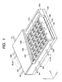
- Fig. 1 is a perspective view of a display panel of the image forming apparatus to which the present invention is applied, in which a part of the panel is cut away in order to show its internal structure.
- reference numeral 1005 denotes a rear plate; 1006, a sidewall; and 1007, a face plate.
- An airtight container for maintaining the inside of the display panel vacuum is formed by the rear plate 1005, the sidewall 1006 and the face plate 1007.
- sealing was attained by applying frit glass on the joining portions and baked for 10 minutes or more under the temperature of 400 to 500°C in the atmosphere or a nitrogen atmosphere.
- a substrate 1001 is fixed to the rear plate 1005, and m ⁇ n pieces of surface conduction electron emission devices are formed on the substrate.
- the numbers m and n are appropriately set according to a target number of display pixels. In this embodiment, it was assumed that m is 3,840 and n is 768.
- FIG. 2 shows a plan view of the multi-electron beam source of the image forming apparatus shown in Fig. 1.
- the surface conduction electron emission devices 1002 as electron-emitting devices are arranged on the substrate 1001. These devices are wired in a passive matrix shape by row direction wiring electrodes 1003 and column direction wiring electrodes 1004.
- Insulating layers are formed between electrodes in parts where the row direction wiring electrodes 1003 and the column direction wiring electrodes 1004 intersect, whereby electric insulation is kept.
- the multi-electron beam source of such a structure is manufactured by feeding power to each device via the row direction wiring electrodes 1003 and the column direction wiring electrodes 1004 to perform an energization forming operation and an energization activation operation after forming the row direction wiring electrodes 1003, the column direction wiring electrodes 1004, the inter-electrodes insulating layers and device electrodes and electroconductive thin films of the surface conduction electron emission devices were formed on the substrate 1001 in advance.
- a fluorescent film 1008 is formed below the face plate 1007 of Fig. 1. Since the image forming apparatus of this embodiment is a color display apparatus, phosphors of three primary colors of red, green and blue, which are used in the field of CRT, are separately coated in parts of the fluorescent film 1008.
- Fig. 3 is a plan view illustrating an arrangement of phosphors on the face plate of the display panel of the image forming apparatus shown in Fig. 1.
- Purposes of providing the black electric conductor 1010 are to prevent dislocation from occurring in displayed colors even if an irradiation position of an electron beam is slightly dislocated, to prevent reflection of external light to keep display contrast from decreasing, to prevent charge-up of a fluorescent film by an electron beam, and the like.
- a way of separately coating the phosphors of three primary colors is not limited to the arrangement of a stripe shape shown in Fig. 3 but may be a delta shaped arrangement or arrangements other than that.
- a metal back 1009 that is well known in the field of CRT is provided on a surface on the rear plate side of the fluorescent film 1008.
- Purposes of providing the metal back 1009 are to perform mirror-reflection of a part of light emitted by the fluorescent film 1008 to improve a light utilization, to protect the fluorescent film 1008 from collision of negative ion, to cause it to act as an electrode for applying an electron beam acceleration voltage, to cause it to act as an electric conduction path of electrons that excite the fluorescent film 1008, and the like.
- the metal back 1009 is formed by a method of forming the fluorescent film 1008 on the face plate 1007 and, then, applying a smoothing operation to the surface of the fluorescent film and depositing Al thereon by vacuum evaporation.
- Dx1 to Dxm, Dy1 to Dyn and Hv are terminals for electric connection of an airtight structure provided for electrically connecting the display panel and an electric circuit (not shown).
- the terminals Dx1 to Dxm, Dy1 to Dyn and Hv are electrically connected to the column direction wiring electrodes 1003 of the electron source, the row direction wiring electrodes 1004 of the electron source and the metal back 1009 of the face plate, respectively.
- an exhaust pipe (not shown) and vacuum pump are connected to evacuate the airtight container to a vacuum degree of approximately 1.0 ⁇ 10 -6 (Pa).
- the getter film is a film that is formed by heating and evaporating a getter material containing, for example, Ba as a main component by a heater or high frequency heating.
- a degree of vacuum in the airtight container is maintained to be approximately 1.0 ⁇ 10 -6 (Pa) by an absorptive action of the getter film. That is, the airtight container is in a stabilized state in which a partial pressure of organic matter is reduced.
- a device subjected to an energization forming operation and an energization activation operation is maintained in a stabilized state in which the partial pressure of organic matter is reduced.
- An electric field intensity in the vicinity of an electron-emitting region that is driving in a surface conduction electron emission device is extremely high.
- an emitted electron amount gradually decreases. Changes over time in the vicinity of the electron-emitting region due to a high electric field intensity is considered to appear as a decrease in an emitted electron amount.
- the preliminary driving means measuring an electric field intensity in the vicinity of an electron-emitting region of a device at the time of driving at a voltage of Vpre after driving a surface conduction electron emission device subjected to a stabilization process at the voltage Vpre.
- Fig. 4 shows a structure of a drive circuit for applying a waveform signal for characteristics adjustment to each surface conduction electron emission device of the display panel 301 to change an electron-emitting characteristic of respective surface conduction electron emission devices of an electron source substrate. That is, Fig. 4 is a schematic diagram of an image forming apparatus using a multi-electron source and a characteristics adjustment apparatus for an image forming apparatus that applies a characteristics adjustment signal to this image forming apparatus.
- reference numeral 301 denotes a display panel, in which a substrate having a plurality of surface conduction electron emission devices arranged in a matrix form, a face plate having phosphors that are provided on the substrate apart from each other and emit light by electrons emitted from the surface conduction electron emission devices, and the like are arranged in a vacuum container.
- the preliminary drive voltage Vpre is applied to each device of the display panel 301 prior to characteristics adjustment.
- Reference numeral 302 denotes a terminal for applying a high voltage from a high voltage source 311 to the phosphors of the display panel 301.
- Reference numerals 303 and 304 denote switch matrices, which select row direction wiring and column direction wiring, respectively, to select an electron-emitting device to which a pulse voltage is applied.
- Reference numerals 306 and 307 denote pulse generation circuits, which generate pulse waveform signals Px and Py for driving.
- Reference numeral 305 denotes a luminance measurement apparatus for capturing light emission of the image forming apparatus to perform photoelectric sensing, which consists of an optical lens 305a and an area sensor 305b.
- a CCD is used as the area sensor 305b.
- a state of light emission of the image forming apparatus is electronically shown as two-dimensional image information using this optical system.
- Reference numeral 308 denotes an arithmetic operation circuit.
- Two-dimensional image information Ixy that is an output of the area sensor 305b and positional information Axy designated in the switch matrices 303 and 304 are inputted in the arithmetic operation circuit 308 from a switch matrix control circuit 310, whereby the arithmetic operation circuit 308 calculates information of a light emission corresponding to each one of the driven surface conduction electron emission devices and outputs the information to a control circuit 312 as Lxy. Details of this method will be described later.
- Reference numeral 309 denotes a robot system for relatively moving the area sensor with respect to the panel, which consists of a ball screw (not shown) and linear guide (not shown).
- Reference numeral 311 denotes a circuit setting a pulse height value, which outputs pulse setting signals Lpx and Lpy, thereby determining a wave height value of pulse signals outputted from the pulse generator circuits 306 and 307, respectively.
- Reference numeral 312 denotes a control circuit, which controls the entire characteristics adjustment flow and outputs data Tv for setting a wave height value in the circuit setting a pulse height value.
- reference numeral 312a denotes a CPU, which controls operations of the control circuit 312.
- Reference numeral 312b denotes a memory storing luminance data for storing light emission characteristics of each device for characteristics adjustment of each device.
- the memory storing luminance data 312b stores light emission data that is proportional to luminance of light emitted by electrons emitted from each device at the time of applying the usual drive voltage Vdrv.
- Reference numeral 312c denotes a memory for storing a characteristic shift voltage required for adjusting characteristics to target set values.
- Reference numeral 312d denotes a lookup table (LUT) that is referred to in order to perform characteristics adjustment of a device, which will be described in detail later.
- LUT lookup table
- Reference numeral 310 denotes a switch matrix control circuit, which outputs switch changeover signals Tx and Ty to control selection of the switch matrices 303 and 304, thereby selecting an electron-emitting device to which a pulse voltage is applied.
- the switch matrix control circuit outputs address information Axy on which device is turned on to the arithmetic operation apparatus 308.
- the luminance measurement apparatus 305 is moved to be positioned opposite to a display panel, on which it is desired to measure light emission luminance, by the robot system 309.
- the switch matrix control circuit 310 controls the switch matrices 303 and 304 to select predetermined row direction wiring or column direction wiring according to a switch matrix control signal Tsw from the control circuit 312, and the row direction wiring or the column direction wiring is switched to be connected such that a surface conduction electron-emitting device of a desired address can be driven.
- control circuit 312 outputs the wave height value data Tv for measuring electron emission characteristics to the circuit setting a pulse height value 311. Consequently, wave height value data Lpx and Lpy are outputted to the respective pulse generation circuits 306 and 307 from the circuit setting a pulse height value 311.
- the respective pulse generation circuits 306 and 307 output drive pulses Px and Py based on the wave height value data Lpx and Lpy, and the drive pulses Px and Py are applied to the device selected by the switch matrices 303 and 304.
- the drive pulses Px and Py are set to have an amplitude of a half of a voltage (wave height value) Vdrv that is applied to a surface conduction electron emission device for characteristics measurement and have different polarities from each other.
- a predetermined voltage is applied to phosphors of the display panel 301 by the high voltage power supply 313.
- a signal Tsync indicating a period of the repeated processes is sent to an area sensor as a trigger of an electronic shutter.
- Fig. 5 is a drive timing chart in the characteristic adjustment apparatus for an image forming apparatus shown in Fig. 4.
- Fig. 6 schematically shows a state described above.
- Fig. 6 is a schematic view showing a state in which bright spots on the image forming apparatus shown in Fig. 4 are projected on an area sensor.
- a reduction ratio of an optical system is set such that an image is focused on a plurality of devices 602 of the area sensor with respect to one light emitting point 601.
- This picked-up image Ixy is transferred to the arithmetic operation apparatus 308. Since images of driven device are focused, if a sum of CCD information allocated corresponding to respective devices is calculated for the number of devices, a luminance value proportional to a light emission amount of the respective driven devices is obtained. Since a luminance value corresponding to the devices of the driven rectangular area is obtained, information is sent to the control circuit 312 as Lxy.
- the electronic shutter is also opened during an afterglow time of phosphors, influence of the afterglow time does not occur between light emitting points because the light emitting points are separated spatially on the area sensor.
- Fig. 7 is a graph showing an example of an emission current characteristic at the time when the drive voltage (wave height value of a drive pulse) Vf of each surface conduction electron emission device, to which the preliminary drive voltage wave height value Vpre is applied, is changed during the process of manufacturing the multi-electron source of the display panel 301 by the characteristic adjustment method for an image forming apparatus in accordance with the present invention.
- Fig. 8 is a graph showing a change in an emission current characteristic at the time when a characteristic shift voltage is applied to a device having the emission current characteristic of (a) in Fig. 7,
- Fig. 9 is a graph showing changes in a wave height value of a characteristic shift pulse voltage (characteristic shift voltage) and an emission current.
- an emission current characteristic of a certain surface conduction electron emission device is shown by an operation curve (a).
- An emission current at the time of the drive voltage Vdrv is Iel in an electron-emitting device having the emission characteristic of the curve (a).
- the surface conduction electron emission device used in this embodiment has an emission current characteristic (memory functionality) corresponding to maximum wave height values and widths of drive pulses of voltages applied in the past.
- Fig. 8 shows how the emission current characteristic changes when the characteristic shift voltage Vshift (Vshift ⁇ Vpre) is applied to a device having the emission current characteristic of (a) in Fig. 7 (curve (c) of Fig. 8).
- the emission current Ie at the time when Vdrv is applied decreases from Ie1 to Ie2 by the application of the characteristic shift voltage. That is, the emission current characteristic shifts in the right direction (in the direction in which an emission current decreases) by the application of the characteristic shift voltage.
- the emission light characteristic can be shifted. In this embodiment, such characteristic adjustment was also performed.
- a light emission characteristic of each electron-emitting device is measured prior to using electron-emitting devices and, if there is fluctuation in electron emission characteristics, the electron emission characteristics are corrected to be uniform.
- a magnitude of a voltage applied to the electron-emitting devices in each process is set as described below.
- VEmeasure a characteristic shift voltage that was applied in a process of adjusting a characteristic of each electron-emitting device to be uniform and a maximum value of a drive voltage that was applied when the electron-emitting device was used
- Vshift is set larger than VEmeasure, a pulse for characteristic shift becomes a largest voltage applied to an electron-emitting device.
- Vshift is set larger than Vdrive, inconvenience in that an electron emission characteristic adjusted to be uniform is shifted during use can be prevented.
- light emission luminance with respect to an electron emission current from a device depends on an acceleration voltage of electrons, a current density and a light emission characteristic of phosphors.
- the robot system was designed such that the area could be scanned, and a magnitude of an optical system was set to 0.18.
- Fig. 10 is a flow chart showing characteristics measurement processing by the control circuit 312. This is a flow chart showing characteristic adjustment processing of each surface conduction electron emission device of an electron source of the first embodiment of the characteristic adjustment method for an image forming apparatus in accordance with the present invention.
- step 1001 a luminance measurement system is moved to a desired sight.
- step 1004 a pulse signal for characteristics measurement of an electron-emitting device is applied to the surface conduction electron emission devices selected in step 1002 from the pulse generation circuit 306 and 307 via the switch matrices 303 and 304.
- step 1006 it is judged whether or not measurement of a luminance value with respect to a predetermined drive voltage is finished.
- a drive voltage was changed to measure luminance for a plurality of times under three conditions of Vdrv, Vdrv - 0.5 Volt and Vdrv - 1 Volt .
- step 1006 The processing from step 1002 to step 1006 is repeated 96 times while sequentially changing row wiring to be designated (step 1007).
- step 1008 the measured luminance is converted into luminance values corresponding to device addresses based on a light emitting image and addresses of driven devices. That is, 384 ⁇ 96 devices were driven and luminance values of the devices could be obtained.
- step 1009 the luminance values are stored in the luminance data storage memory 312b.
- step 1010 processing of applying a shift voltage is performed. Details of this step will be described later. Up to this stage, processing of applying a shift voltage is finished for one sight.
- step 1011 it is checked if the luminance measurement and the processing of applying a shift voltage are finished for all the sights of the display panel 1. If not finished, the processing advances to step 1001, where the optical system is moved to the next sight and the processing is repeated.
- the robot system 309 was used for the movement of the optical system, while the luminance measurement system was moved at the speed of 30 mm/sec.
- the drive time is 0.15 second. Since the moving time was four seconds per one sight and there were 80 sights, the total moving time was approximately 320 seconds.
- the CPU 312a reads data of a device, which has an initial characteristic most approximate to that of the device, out of the lookup table 312d.
- the CPU 312a measures changes Vf to measure luminance to find approximate curves of the luminance and compares approximate coefficients of the luminance to select data with values approximate to each other.
- the CPU 312a selects a characteristic shift voltage for equalizing a characteristic of the device to the target value out of the data.
- a relationship between an emission current and luminance is also determined substantially uniquely.
- a change in luminance with respect to a change in the device drive voltage Vf is an initial characteristic in the present invention.
- a wave height value of a pulse signal is set in the circuit setting a pulse wave height value 311 through a wave height value set signal Tv.
- the circuit setting a pulse wave height value 311 outputs the wave height value data Lpx and Lpy, and the pulse generation circuits 306 and 307 output the drive pulses Px and Py of the set wave height value based on the value.
- a value of a characteristic shift voltage is determined for respective devices, and a characteristic shift pulse, which corresponds to a characteristic of a surface conduction electron emission device for which the characteristic should be shifted, is applied to the surface conduction electron emission device (step 1105).
- step 1106 it is checked if the processing for all the surface conduction electron emission devices within one sight is finished. If not finished, the next device is selected (step 1107) and the processing returns to step 1101.
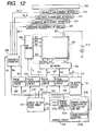
- Fig. 12 shows a structure of an apparatus for arranging an electron emitting characteristic of each surface conduction electron emission device of the display panel 301 along a certain target set value.
- Luminance measurement systems 314, 315 and 316 and pulse generation circuits 317 and 318 are added to the structure shown in Fig. 4.
- Fig. 12 is a schematic diagram of an image forming apparatus using a multi-electron source and a characteristic adjustment apparatus for an image forming apparatus for applying a characteristic adjustment signal to this image forming apparatus, which are used in the second embodiment of the characteristic adjustment method for an image forming apparatus in accordance with the present invention.
- acceleration of processing is realized by providing four sights that are selected at a time.
- Fig. 13 is a perspective view showing a structure of the characteristic adjustment apparatus in the second embodiment of the characteristic adjustment method for an image forming apparatus in accordance with the present invention.
- the display panel 301 is placed on a stage 1301 and a robot system 1303 for moving an optical system in X and Y directions is arranged on a pedestal 1302 as illustrated in the schematic view shown in Fig. 13.
- the optical system consists of a lens 1304 and a CCD camera 1305, and four optical systems are arranged.
- Fig. 15 is a schematic view showing sight positions that are set in the image forming apparatus in the second embodiment of the characteristic adjustment method for an image forming apparatus in accordance with the present invention.
- step 1402 the switch matrix control signal Tsw is outputted, and switch matrices 303 and 304 are switched by the switch matrix control circuit 310 to select 768 surface conduction electron emission devices of the display panel 301.
- step 1403 wave height value data Tv1 and Tv2 of a pulse signal applied to the selected devices are outputted to the circuit setting a pulse wave height value 311.
- step 1404 a pulse signal for characteristics measurement of an electron-emitting device is applied to the surface conduction electron emission devices selected in step 1402 by the pulse generation circuits 306, 307, 317 and 318 via the switch matrices 303 and 304.
- step 1405 luminance with respect to a drive voltage is measured.
- step 1406 it is judged whether or not measurement of a luminance value with respect to a predetermined drive voltage is finished.
- a drive voltage was changed to measure luminance for a plurality of times under three kinds of conditions, Vdrv, Vdrv - 0.5 Volt and Vdrv - 1 Volt.
- step 1405 If the luminance measurement by the predetermined drive voltage is not finished, the processing from step 1402 to step 1405 is repeated until the luminance measurement by the predetermined drive voltage is finished. If the luminance measurement by the predetermined drive voltage is finished, the processing moves to step 1407.
- step 1403 to step 1406 The processing from step 1403 to step 1406 is repeated 96 times while sequentially increasing the number of designated row wirings (Y) (step 1407).
- the synchronizing signal Tsync in synchronous with the lighting of these rectangular areas is outputted from the control circuit 312, and the electronic shutter is opened based on the signal. Consequently, a light emitting image in the area driven in step 1405 is measured.
- Characteristics of devices vary when a shift voltage is applied to devices other than a device to be adjusted. This problem was avoided in this embodiment in the following manner.
- a voltage applied from a Y side of the sights 1 and 2 is Py1
- a voltage applied from an X side of the sights 1 and 2 is Px1
- a voltage applied from a Y side of the sights 3 and 4 is Py2
- voltage applied form an X side of the sights 3 and 4 is Px2
- a voltage of Py1 + Px1 is applied to devices in the sight 1.
- a voltage of Py2 + Px1 is applied to devices in the sight 2.
- a voltage of Py1 + Px2 is applied to devices in the sight 3.
- a voltage of Py2 + Px2 is applied to devices in the sight 2.
- instruction signals Lp1, Lp2, Lp3 and Lp4 were determined such that the four types of voltages became the Vdrv voltages in measuring luminance.
- luminance data is stored in a luminance data storage memory (step 1409) and processing of applying a shift voltage is performed (step 1410). Then, it is checked if the luminance measurement and the processing of applying a shift voltage are finished for all the sights (step 1411) and, if finished, the operations are finished.
- Fig. 16 is a flow chart showing processing for applying a characteristic adjustment signal in the second embodiment of the characteristic adjustment method for an image forming apparatus in accordance with the present invention.
- one device for two sights, respectively, total two devices are selected, and a shift voltage is applied to the devices simultaneously.
- the shift voltage is not applied to one device for four sights, respectively, total four devices, due to the following reasons.
- step 1601 luminance data of devices of addresses corresponding to the respective sights 1 and 3 is read.
- the devices are assumed to be A and B.
- the luminance data for A is compared with a target value and presence or absence of application of a V shift voltage is judged.
- step 1602 It is judged whether or not application of a shift voltage is required (step 1602). If the application is required, in step 1603, a shift voltage Tv1 is determined with reference to a lookup table.
- step 1604 presence or absence of shift voltage application to the device B is judged and, in step 1605, Tv2 is determined.
- the instruction signals Lp1, Lp2, Lp3 and Lp4 are determined. Then, devices to be selected are selected from the sight 2 and the sight 4 to perform the processing of applying a shift voltage sequentially.
- devices are selected in step 1606 using the above-mentioned voltage setting and, in step 1607, a shift voltage is actually applied.
- Time required for measuring luminance values of the entire screen was approximately 80 second that was one fourth of that in the first embodiment.
- application time of the shift voltage could be reduced to 3,000 seconds that was one half of that in the first embodiment.
- a characteristic adjustment method for an image forming apparatus that is provided with a multi-electron source in which a plurality of electron-emitting devices are electrically connected by wiring and arranged on a substrate and a fluorescent member for emitting light by irradiation of an electron beam, the method including: a measurement step of dividing a display portion of the image forming apparatus into a plurality of areas and measuring light emitting characteristics of at least one or more of the electron-emitting devices in the respective divided areas, and a shifting step of shifting the light emitting characteristics of the electron-emitting devices in the divided areas to individual characteristic target values by applying a characteristic shift voltage to the electron-emitting devices.
Landscapes
- Engineering & Computer Science (AREA)
- Physics & Mathematics (AREA)
- Computer Hardware Design (AREA)
- General Physics & Mathematics (AREA)
- Theoretical Computer Science (AREA)
- Manufacturing & Machinery (AREA)
- Cold Cathode And The Manufacture (AREA)
- Manufacture Of Electron Tubes, Discharge Lamp Vessels, Lead-In Wires, And The Like (AREA)
- Control Of Indicators Other Than Cathode Ray Tubes (AREA)
Applications Claiming Priority (2)
| Application Number | Priority Date | Filing Date | Title |
|---|---|---|---|
| JP2001304610A JP5022547B2 (ja) | 2001-09-28 | 2001-09-28 | 画像形成装置の特性調整方法、画像形成装置の製造方法、画像形成装置及び特性調整装置 |
| JP2001304610 | 2001-09-28 |
Publications (2)
| Publication Number | Publication Date |
|---|---|
| EP1298698A1 true EP1298698A1 (fr) | 2003-04-02 |
| EP1298698B1 EP1298698B1 (fr) | 2010-07-28 |
Family
ID=19124505
Family Applications (1)
| Application Number | Title | Priority Date | Filing Date |
|---|---|---|---|
| EP02021675A Expired - Lifetime EP1298698B1 (fr) | 2001-09-28 | 2002-09-27 | Procédé et appareil d'ajustement de caractéristiques d'un dispositif de formation d'images et procédé de fabrication d'un dispositif de formation d'images |
Country Status (6)
| Country | Link |
|---|---|
| US (2) | US6888519B2 (fr) |
| EP (1) | EP1298698B1 (fr) |
| JP (1) | JP5022547B2 (fr) |
| KR (1) | KR100479944B1 (fr) |
| CN (1) | CN1249766C (fr) |
| DE (1) | DE60237136D1 (fr) |
Families Citing this family (17)
| Publication number | Priority date | Publication date | Assignee | Title |
|---|---|---|---|---|
| JP4115330B2 (ja) | 2002-05-08 | 2008-07-09 | キヤノン株式会社 | 画像形成装置の製造方法 |
| JP4027284B2 (ja) * | 2002-07-26 | 2007-12-26 | キヤノン株式会社 | 画像表示装置の製造方法 |
| TW577136B (en) * | 2002-10-25 | 2004-02-21 | Ritdisplay Corp | Detecting repairing system and method |
| KR100517960B1 (ko) * | 2003-04-18 | 2005-09-30 | 엘지전자 주식회사 | 전계방출 소자 스페이서 방전 장치 및 방법 |
| JP3962728B2 (ja) * | 2003-06-20 | 2007-08-22 | キヤノン株式会社 | 画像表示装置 |
| JP2005257791A (ja) * | 2004-03-09 | 2005-09-22 | Canon Inc | 画像表示装置及び画像表示装置の駆動方法 |
| JP4352025B2 (ja) | 2004-06-29 | 2009-10-28 | キヤノン株式会社 | 画像表示装置 |
| JP3870214B2 (ja) * | 2004-06-29 | 2007-01-17 | キヤノン株式会社 | 補正回路 |
| US7592743B2 (en) | 2004-12-27 | 2009-09-22 | Canon Kabushiki Kaisha | Compensation of warping in display apparatus substrate |
| KR100769428B1 (ko) * | 2005-04-28 | 2007-10-22 | 삼성에스디아이 주식회사 | 발광표시장치와 발광 표시장치의 휘도수치화 장치 및휘도수치화 방법 |
| JP4600190B2 (ja) * | 2005-07-15 | 2010-12-15 | 双葉電子工業株式会社 | 電界放出表示素子を用いた表示装置、電界放出表示素子の輝度調整装置およびその輝度調整方法 |
| JP2008158285A (ja) * | 2006-12-25 | 2008-07-10 | Canon Inc | 画像表示装置 |
| US8169133B2 (en) * | 2006-12-27 | 2012-05-01 | Canon Kabushiki Kaisha | Image display apparatus, manufacturing method of image display apparatus, and functional film |
| FR2925349A1 (fr) * | 2007-12-20 | 2009-06-26 | Applexion | Procede de separation sequence multicolonnes d'un derive metallique ionique |
| JP2010090231A (ja) * | 2008-10-07 | 2010-04-22 | Canon Inc | 画像表示装置 |
| JP2010243775A (ja) * | 2009-04-06 | 2010-10-28 | Canon Inc | 補正値の取得方法、補正方法、画像表示装置 |
| JP7119201B2 (ja) * | 2019-02-26 | 2022-08-16 | 京セラ株式会社 | 発光素子基板、表示装置および表示装置のリペア方法 |
Citations (9)
| Publication number | Priority date | Publication date | Assignee | Title |
|---|---|---|---|---|
| US5581159A (en) | 1992-04-07 | 1996-12-03 | Micron Technology, Inc. | Back-to-back diode current regulator for field emission display |
| EP0755042A1 (fr) * | 1995-07-20 | 1997-01-22 | STMicroelectronics S.r.l. | Méthode et dispositif pour uniformiser la luminosité et pour réduire la dégradation de la matière fluorescente dans un dispositif d'affichage plat à émission de champ |
| US5656892A (en) * | 1995-11-17 | 1997-08-12 | Micron Display Technology, Inc. | Field emission display having emitter control with current sensing feedback |
| EP0803892A2 (fr) | 1996-02-23 | 1997-10-29 | Canon Kabushiki Kaisha | Dispositif générateur d'électrons, dispositif de formation d'images, procédé de fabrication et procédé de réglage de ses caractéristiques |
| JPH10228867A (ja) * | 1996-02-23 | 1998-08-25 | Canon Inc | 電子発生装置、画像形成装置及びそれらの製造方法及び特性調整方法 |
| JPH11133911A (ja) * | 1997-10-24 | 1999-05-21 | Canon Inc | 画像形成方法及び装置 |
| US6031344A (en) * | 1998-03-24 | 2000-02-29 | Motorola, Inc. | Method for driving a field emission display including feedback control |
| US6231412B1 (en) * | 1996-09-18 | 2001-05-15 | Canon Kabushiki Kaisha | Method of manufacturing and adjusting electron source array |
| JP2001209352A (ja) * | 2000-01-24 | 2001-08-03 | Nec Corp | 電界電子放出型ディスプレィ装置およびその駆動方法 |
Family Cites Families (25)
| Publication number | Priority date | Publication date | Assignee | Title |
|---|---|---|---|---|
| JPH05347776A (ja) * | 1992-06-15 | 1993-12-27 | Matsushita Electric Ind Co Ltd | 垂直ランディングズレ量測定装置 |
| CA2138363C (fr) * | 1993-12-22 | 1999-06-22 | Yasuyuki Todokoro | Dispositif generateur de faisceau electronique, dispositif d'affichage d'images et methode d'attaque de ces dispositifs |
| JP3311201B2 (ja) * | 1994-06-08 | 2002-08-05 | キヤノン株式会社 | 画像形成装置 |
| JP3251466B2 (ja) | 1994-06-13 | 2002-01-28 | キヤノン株式会社 | 複数の冷陰極素子を備えた電子線発生装置、並びにその駆動方法、並びにそれを応用した画像形成装置 |
| US6621475B1 (en) * | 1996-02-23 | 2003-09-16 | Canon Kabushiki Kaisha | Electron generating apparatus, image forming apparatus, method of manufacturing the same and method of adjusting characteristics thereof |
| JPH09258687A (ja) * | 1996-03-18 | 1997-10-03 | Canon Inc | 画像形成装置及びその発光特性の変化防止方法 |
| JP3134772B2 (ja) * | 1996-04-16 | 2001-02-13 | 双葉電子工業株式会社 | 電界放出型表示素子およびその駆動方法 |
| JP3199682B2 (ja) * | 1997-03-21 | 2001-08-20 | キヤノン株式会社 | 電子放出装置及びそれを用いた画像形成装置 |
| JP3710273B2 (ja) * | 1997-12-08 | 2005-10-26 | キヤノン株式会社 | 電子源及び画像形成装置の製造方法 |
| US6534924B1 (en) * | 1998-03-31 | 2003-03-18 | Canon Kabushiki Kaisha | Method and apparatus for manufacturing electron source, and method manufacturing image forming apparatus |
| KR100434525B1 (ko) * | 1998-04-10 | 2004-07-16 | 삼성에스디아이 주식회사 | 전계방출 표시소자의 특성 측정 시스템 |
| JP3305283B2 (ja) * | 1998-05-01 | 2002-07-22 | キヤノン株式会社 | 画像表示装置及び前記装置の制御方法 |
| JP2000020020A (ja) * | 1998-06-26 | 2000-01-21 | Canon Inc | 電子源駆動装置及び画像形成装置及び電子源の電子放出特性の補正方法 |
| JP2000243256A (ja) * | 1999-02-22 | 2000-09-08 | Canon Inc | マルチ電子源及び電子発生装置の特性調整方法及び製造方法 |
| JP2000243287A (ja) * | 1999-02-23 | 2000-09-08 | Canon Inc | 電子放出素子の検査装置及び検査方法 |
| JP2000251733A (ja) * | 1999-02-24 | 2000-09-14 | Canon Inc | 電子源および画像形成装置の検査方法及び検査装置及び記録媒体 |
| JP3840027B2 (ja) * | 1999-02-26 | 2006-11-01 | キヤノン株式会社 | 画像表示装置及び表示制御方法 |
| JP2000251688A (ja) * | 1999-02-26 | 2000-09-14 | Canon Inc | 電子源及び電子発生装置の特性調整方法及び製造方法 |
| JP3754885B2 (ja) * | 1999-11-05 | 2006-03-15 | キヤノン株式会社 | フェースプレートの製造方法、画像形成装置の製造方法及び画像形成装置 |
| US6528951B2 (en) * | 2000-06-13 | 2003-03-04 | Semiconductor Energy Laboratory Co., Ltd. | Display device |
| JP3673761B2 (ja) * | 2001-02-09 | 2005-07-20 | キヤノン株式会社 | 電子源の特性調整方法及び電子源の製造方法及び画像表示装置の特性調整方法及び画像表示装置の製造方法 |
| US6712660B2 (en) * | 2001-08-06 | 2004-03-30 | Canon Kabushiki Kaisha | Method and apparatus for adjusting characteristics of electron source, and method for manufacturing electron source |
| JP3667264B2 (ja) * | 2001-08-27 | 2005-07-06 | キヤノン株式会社 | マルチ電子源の特性調整方法及び装置ならびにマルチ電子源の製造方法 |
| JP4115330B2 (ja) * | 2002-05-08 | 2008-07-09 | キヤノン株式会社 | 画像形成装置の製造方法 |
| JP4027284B2 (ja) * | 2002-07-26 | 2007-12-26 | キヤノン株式会社 | 画像表示装置の製造方法 |
-
2001
- 2001-09-28 JP JP2001304610A patent/JP5022547B2/ja not_active Expired - Fee Related
-
2002
- 2002-09-23 US US10/252,038 patent/US6888519B2/en not_active Expired - Fee Related
- 2002-09-26 CN CNB021323801A patent/CN1249766C/zh not_active Expired - Fee Related
- 2002-09-27 EP EP02021675A patent/EP1298698B1/fr not_active Expired - Lifetime
- 2002-09-27 KR KR10-2002-0058614A patent/KR100479944B1/ko not_active Expired - Fee Related
- 2002-09-27 DE DE60237136T patent/DE60237136D1/de not_active Expired - Lifetime
-
2005
- 2005-02-04 US US11/049,996 patent/US7388561B2/en not_active Expired - Fee Related
Patent Citations (10)
| Publication number | Priority date | Publication date | Assignee | Title |
|---|---|---|---|---|
| US5581159A (en) | 1992-04-07 | 1996-12-03 | Micron Technology, Inc. | Back-to-back diode current regulator for field emission display |
| EP0755042A1 (fr) * | 1995-07-20 | 1997-01-22 | STMicroelectronics S.r.l. | Méthode et dispositif pour uniformiser la luminosité et pour réduire la dégradation de la matière fluorescente dans un dispositif d'affichage plat à émission de champ |
| US5656892A (en) * | 1995-11-17 | 1997-08-12 | Micron Display Technology, Inc. | Field emission display having emitter control with current sensing feedback |
| EP0803892A2 (fr) | 1996-02-23 | 1997-10-29 | Canon Kabushiki Kaisha | Dispositif générateur d'électrons, dispositif de formation d'images, procédé de fabrication et procédé de réglage de ses caractéristiques |
| JPH10228867A (ja) * | 1996-02-23 | 1998-08-25 | Canon Inc | 電子発生装置、画像形成装置及びそれらの製造方法及び特性調整方法 |
| US6231412B1 (en) * | 1996-09-18 | 2001-05-15 | Canon Kabushiki Kaisha | Method of manufacturing and adjusting electron source array |
| JPH11133911A (ja) * | 1997-10-24 | 1999-05-21 | Canon Inc | 画像形成方法及び装置 |
| US6031344A (en) * | 1998-03-24 | 2000-02-29 | Motorola, Inc. | Method for driving a field emission display including feedback control |
| JP2001209352A (ja) * | 2000-01-24 | 2001-08-03 | Nec Corp | 電界電子放出型ディスプレィ装置およびその駆動方法 |
| US20020008482A1 (en) * | 2000-01-24 | 2002-01-24 | Nec Corporation | Field emission display and method of driving the same |
Non-Patent Citations (2)
| Title |
|---|
| PATENT ABSTRACTS OF JAPAN vol. 1999, no. 10 31 August 1999 (1999-08-31) * |
| PATENT ABSTRACTS OF JAPAN vol. 2000, no. 25 12 April 2001 (2001-04-12) * |
Also Published As
| Publication number | Publication date |
|---|---|
| US20030083843A1 (en) | 2003-05-01 |
| CN1249766C (zh) | 2006-04-05 |
| US6888519B2 (en) | 2005-05-03 |
| US20050148272A1 (en) | 2005-07-07 |
| KR20030027771A (ko) | 2003-04-07 |
| CN1411014A (zh) | 2003-04-16 |
| DE60237136D1 (de) | 2010-09-09 |
| JP2003109508A (ja) | 2003-04-11 |
| US7388561B2 (en) | 2008-06-17 |
| KR100479944B1 (ko) | 2005-04-07 |
| JP5022547B2 (ja) | 2012-09-12 |
| EP1298698B1 (fr) | 2010-07-28 |
Similar Documents
| Publication | Publication Date | Title |
|---|---|---|
| EP1298698B1 (fr) | Procédé et appareil d'ajustement de caractéristiques d'un dispositif de formation d'images et procédé de fabrication d'un dispositif de formation d'images | |
| US6760001B2 (en) | Method of adjusting characteristics of electron source, method of manufacturing electron emission device | |
| US7924243B2 (en) | Image display apparatus for forming an image with a plurality of luminescent points | |
| JP4027284B2 (ja) | 画像表示装置の製造方法 | |
| US20060061593A1 (en) | Image display unit and method of correcting brightness in image display unit | |
| CN100493139C (zh) | 显示器校正系统 | |
| US20100079506A1 (en) | Image display apparatus | |
| JPH08234690A (ja) | 電子発生装置と画像表示装置、それらの駆動方法および駆動回路 | |
| JP2004185828A (ja) | 電子源および画像表示装置の特性調整方法および特性調整装置 | |
| JPH09258687A (ja) | 画像形成装置及びその発光特性の変化防止方法 | |
| JP4194622B2 (ja) | 画像表示装置 | |
| JPH07181918A (ja) | 画像表示装置の駆動方法 | |
| JP2000066634A (ja) | 電子源駆動装置及び画像形成装置及び電子源の駆動方法 | |
| JPH077709A (ja) | 画像表示装置の自動調整装置 | |
| JPH0973278A (ja) | マルチ電子源の駆動方法及び装置、及びそれを用いた画像形成装置 | |
| JP2006084566A (ja) | 表示装置の製造方法、表示装置の製造装置および平面表示装置 | |
| JPH08221030A (ja) | 電子源の駆動装置、画像形成装置およびそれらの方法 | |
| JPH10123997A (ja) | 電子源と該電子源を用いた画像形成装置 | |
| JPH09134146A (ja) | 電子源の駆動装置、画像形成装置およびそれらの方法 |
Legal Events
| Date | Code | Title | Description |
|---|---|---|---|
| PUAI | Public reference made under article 153(3) epc to a published international application that has entered the european phase |
Free format text: ORIGINAL CODE: 0009012 |
|
| AK | Designated contracting states |
Kind code of ref document: A1 Designated state(s): AT BE BG CH CY CZ DE DK EE ES FI FR GB GR IE IT LI LU MC NL PT SE SK TR Designated state(s): AT BE BG CH CY CZ DE DK EE ES FI FR GB GR IE IT LI LU MC NL PT SE SK TR |
|
| AX | Request for extension of the european patent |
Extension state: AL LT LV MK RO SI |
|
| 17P | Request for examination filed |
Effective date: 20030814 |
|
| AKX | Designation fees paid |
Designated state(s): DE FR GB IT NL |
|
| 17Q | First examination report despatched |
Effective date: 20061120 |
|
| GRAP | Despatch of communication of intention to grant a patent |
Free format text: ORIGINAL CODE: EPIDOSNIGR1 |
|
| GRAS | Grant fee paid |
Free format text: ORIGINAL CODE: EPIDOSNIGR3 |
|
| GRAA | (expected) grant |
Free format text: ORIGINAL CODE: 0009210 |
|
| AK | Designated contracting states |
Kind code of ref document: B1 Designated state(s): DE FR GB IT NL |
|
| REG | Reference to a national code |
Ref country code: GB Ref legal event code: FG4D |
|
| REF | Corresponds to: |
Ref document number: 60237136 Country of ref document: DE Date of ref document: 20100909 Kind code of ref document: P |
|
| REG | Reference to a national code |
Ref country code: NL Ref legal event code: VDEP Effective date: 20100728 |
|
| PG25 | Lapsed in a contracting state [announced via postgrant information from national office to epo] |
Ref country code: NL Free format text: LAPSE BECAUSE OF FAILURE TO SUBMIT A TRANSLATION OF THE DESCRIPTION OR TO PAY THE FEE WITHIN THE PRESCRIBED TIME-LIMIT Effective date: 20100728 |
|
| PG25 | Lapsed in a contracting state [announced via postgrant information from national office to epo] |
Ref country code: IT Free format text: LAPSE BECAUSE OF FAILURE TO SUBMIT A TRANSLATION OF THE DESCRIPTION OR TO PAY THE FEE WITHIN THE PRESCRIBED TIME-LIMIT Effective date: 20100728 |
|
| PLBE | No opposition filed within time limit |
Free format text: ORIGINAL CODE: 0009261 |
|
| STAA | Information on the status of an ep patent application or granted ep patent |
Free format text: STATUS: NO OPPOSITION FILED WITHIN TIME LIMIT |
|
| 26N | No opposition filed |
Effective date: 20110429 |
|
| REG | Reference to a national code |
Ref country code: DE Ref legal event code: R097 Ref document number: 60237136 Country of ref document: DE Effective date: 20110429 |
|
| PGFP | Annual fee paid to national office [announced via postgrant information from national office to epo] |
Ref country code: GB Payment date: 20120926 Year of fee payment: 11 |
|
| PGFP | Annual fee paid to national office [announced via postgrant information from national office to epo] |
Ref country code: DE Payment date: 20120930 Year of fee payment: 11 |
|
| PGFP | Annual fee paid to national office [announced via postgrant information from national office to epo] |
Ref country code: FR Payment date: 20121009 Year of fee payment: 11 |
|
| GBPC | Gb: european patent ceased through non-payment of renewal fee |
Effective date: 20130927 |
|
| REG | Reference to a national code |
Ref country code: DE Ref legal event code: R119 Ref document number: 60237136 Country of ref document: DE Effective date: 20140401 |
|
| REG | Reference to a national code |
Ref country code: FR Ref legal event code: ST Effective date: 20140530 |
|
| PG25 | Lapsed in a contracting state [announced via postgrant information from national office to epo] |
Ref country code: GB Free format text: LAPSE BECAUSE OF NON-PAYMENT OF DUE FEES Effective date: 20130927 |
|
| PG25 | Lapsed in a contracting state [announced via postgrant information from national office to epo] |
Ref country code: DE Free format text: LAPSE BECAUSE OF NON-PAYMENT OF DUE FEES Effective date: 20140401 Ref country code: FR Free format text: LAPSE BECAUSE OF NON-PAYMENT OF DUE FEES Effective date: 20130930 |