EP1302968A2 - Procédé de fabrication d'un dispositif émetteur d'électrons, d'une source d'électrons et d'un appareil de formation d'images - Google Patents
Procédé de fabrication d'un dispositif émetteur d'électrons, d'une source d'électrons et d'un appareil de formation d'images Download PDFInfo
- Publication number
- EP1302968A2 EP1302968A2 EP02022696A EP02022696A EP1302968A2 EP 1302968 A2 EP1302968 A2 EP 1302968A2 EP 02022696 A EP02022696 A EP 02022696A EP 02022696 A EP02022696 A EP 02022696A EP 1302968 A2 EP1302968 A2 EP 1302968A2
- Authority
- EP
- European Patent Office
- Prior art keywords
- electron
- polymer film
- emitting device
- manufacturing
- resistance
- Prior art date
- Legal status (The legal status is an assumption and is not a legal conclusion. Google has not performed a legal analysis and makes no representation as to the accuracy of the status listed.)
- Withdrawn
Links
- 238000004519 manufacturing process Methods 0.000 title claims abstract description 55
- 238000000034 method Methods 0.000 title claims description 64
- 229920006254 polymer film Polymers 0.000 claims abstract description 116
- 239000000758 substrate Substances 0.000 claims abstract description 70
- 239000000463 material Substances 0.000 claims abstract description 22
- 238000000059 patterning Methods 0.000 claims abstract description 8
- 229920001721 polyimide Polymers 0.000 claims description 37
- 238000010894 electron beam technology Methods 0.000 claims description 23
- 230000001678 irradiating effect Effects 0.000 claims description 12
- 238000010438 heat treatment Methods 0.000 claims description 7
- 238000010884 ion-beam technique Methods 0.000 claims description 4
- 239000012298 atmosphere Substances 0.000 abstract description 20
- 238000005304 joining Methods 0.000 abstract description 8
- 230000000717 retained effect Effects 0.000 abstract description 2
- 239000004642 Polyimide Substances 0.000 description 27
- 230000008569 process Effects 0.000 description 26
- OKTJSMMVPCPJKN-UHFFFAOYSA-N Carbon Chemical compound [C] OKTJSMMVPCPJKN-UHFFFAOYSA-N 0.000 description 21
- 229910052799 carbon Inorganic materials 0.000 description 21
- 239000000243 solution Substances 0.000 description 20
- 239000011159 matrix material Substances 0.000 description 13
- SECXISVLQFMRJM-UHFFFAOYSA-N N-Methylpyrrolidone Chemical compound CN1CCCC1=O SECXISVLQFMRJM-UHFFFAOYSA-N 0.000 description 11
- 239000002243 precursor Substances 0.000 description 11
- IJGRMHOSHXDMSA-UHFFFAOYSA-N Atomic nitrogen Chemical compound N#N IJGRMHOSHXDMSA-UHFFFAOYSA-N 0.000 description 10
- VYPSYNLAJGMNEJ-UHFFFAOYSA-N Silicium dioxide Chemical compound O=[Si]=O VYPSYNLAJGMNEJ-UHFFFAOYSA-N 0.000 description 10
- 229920000642 polymer Polymers 0.000 description 10
- 238000007789 sealing Methods 0.000 description 10
- 239000002904 solvent Substances 0.000 description 10
- YXFVVABEGXRONW-UHFFFAOYSA-N Toluene Chemical compound CC1=CC=CC=C1 YXFVVABEGXRONW-UHFFFAOYSA-N 0.000 description 9
- 239000011521 glass Substances 0.000 description 9
- BASFCYQUMIYNBI-UHFFFAOYSA-N platinum Chemical compound [Pt] BASFCYQUMIYNBI-UHFFFAOYSA-N 0.000 description 9
- 239000010410 layer Substances 0.000 description 8
- 229910052751 metal Inorganic materials 0.000 description 8
- 239000002184 metal Substances 0.000 description 8
- 238000007639 printing Methods 0.000 description 8
- 125000006850 spacer group Chemical group 0.000 description 8
- XLYOFNOQVPJJNP-UHFFFAOYSA-N water Substances O XLYOFNOQVPJJNP-UHFFFAOYSA-N 0.000 description 8
- KFZMGEQAYNKOFK-UHFFFAOYSA-N Isopropanol Chemical compound CC(C)O KFZMGEQAYNKOFK-UHFFFAOYSA-N 0.000 description 6
- ZMXDDKWLCZADIW-UHFFFAOYSA-N N,N-Dimethylformamide Chemical compound CN(C)C=O ZMXDDKWLCZADIW-UHFFFAOYSA-N 0.000 description 6
- 125000003118 aryl group Chemical group 0.000 description 6
- 238000000354 decomposition reaction Methods 0.000 description 6
- 238000011161 development Methods 0.000 description 6
- 239000000203 mixture Substances 0.000 description 6
- 229910052757 nitrogen Inorganic materials 0.000 description 6
- 229920005575 poly(amic acid) Polymers 0.000 description 6
- 238000002360 preparation method Methods 0.000 description 6
- 238000007650 screen-printing Methods 0.000 description 6
- OAICVXFJPJFONN-UHFFFAOYSA-N Phosphorus Chemical compound [P] OAICVXFJPJFONN-UHFFFAOYSA-N 0.000 description 5
- GTDPSWPPOUPBNX-UHFFFAOYSA-N ac1mqpva Chemical compound CC12C(=O)OC(=O)C1(C)C1(C)C2(C)C(=O)OC1=O GTDPSWPPOUPBNX-UHFFFAOYSA-N 0.000 description 5
- -1 aromatic diamine compound Chemical class 0.000 description 5
- 239000012153 distilled water Substances 0.000 description 5
- 239000002075 main ingredient Substances 0.000 description 5
- 238000005259 measurement Methods 0.000 description 5
- CSCPPACGZOOCGX-UHFFFAOYSA-N Acetone Chemical compound CC(C)=O CSCPPACGZOOCGX-UHFFFAOYSA-N 0.000 description 4
- HEDRZPFGACZZDS-UHFFFAOYSA-N Chloroform Chemical compound ClC(Cl)Cl HEDRZPFGACZZDS-UHFFFAOYSA-N 0.000 description 4
- FXHOOIRPVKKKFG-UHFFFAOYSA-N N,N-Dimethylacetamide Chemical compound CN(C)C(C)=O FXHOOIRPVKKKFG-UHFFFAOYSA-N 0.000 description 4
- 230000004913 activation Effects 0.000 description 4
- 125000004432 carbon atom Chemical group C* 0.000 description 4
- 230000006872 improvement Effects 0.000 description 4
- 239000003960 organic solvent Substances 0.000 description 4
- 238000004528 spin coating Methods 0.000 description 4
- WGTYBPLFGIVFAS-UHFFFAOYSA-M tetramethylammonium hydroxide Chemical compound [OH-].C[N+](C)(C)C WGTYBPLFGIVFAS-UHFFFAOYSA-M 0.000 description 4
- DPBJAVGHACCNRL-UHFFFAOYSA-N 2-(dimethylamino)ethyl prop-2-enoate Chemical compound CN(C)CCOC(=O)C=C DPBJAVGHACCNRL-UHFFFAOYSA-N 0.000 description 3
- LFQSCWFLJHTTHZ-UHFFFAOYSA-N Ethanol Chemical compound CCO LFQSCWFLJHTTHZ-UHFFFAOYSA-N 0.000 description 3
- 230000015572 biosynthetic process Effects 0.000 description 3
- 239000004020 conductor Substances 0.000 description 3
- 230000005684 electric field Effects 0.000 description 3
- 239000007772 electrode material Substances 0.000 description 3
- 125000005462 imide group Chemical group 0.000 description 3
- 239000011810 insulating material Substances 0.000 description 3
- 229910052697 platinum Inorganic materials 0.000 description 3
- 230000005855 radiation Effects 0.000 description 3
- 239000000126 substance Substances 0.000 description 3
- UXVMQQNJUSDDNG-UHFFFAOYSA-L Calcium chloride Chemical compound [Cl-].[Cl-].[Ca+2] UXVMQQNJUSDDNG-UHFFFAOYSA-L 0.000 description 2
- IAZDPXIOMUYVGZ-UHFFFAOYSA-N Dimethylsulphoxide Chemical compound CS(C)=O IAZDPXIOMUYVGZ-UHFFFAOYSA-N 0.000 description 2
- UFWIBTONFRDIAS-UHFFFAOYSA-N Naphthalene Chemical compound C1=CC=CC2=CC=CC=C21 UFWIBTONFRDIAS-UHFFFAOYSA-N 0.000 description 2
- ATUOYWHBWRKTHZ-UHFFFAOYSA-N Propane Chemical compound CCC ATUOYWHBWRKTHZ-UHFFFAOYSA-N 0.000 description 2
- 239000007864 aqueous solution Substances 0.000 description 2
- 239000012965 benzophenone Substances 0.000 description 2
- 230000005540 biological transmission Effects 0.000 description 2
- 239000001110 calcium chloride Substances 0.000 description 2
- 229910001628 calcium chloride Inorganic materials 0.000 description 2
- 238000007334 copolymerization reaction Methods 0.000 description 2
- 238000005520 cutting process Methods 0.000 description 2
- 229910001873 dinitrogen Inorganic materials 0.000 description 2
- ZUOUZKKEUPVFJK-UHFFFAOYSA-N diphenyl Chemical compound C1=CC=CC=C1C1=CC=CC=C1 ZUOUZKKEUPVFJK-UHFFFAOYSA-N 0.000 description 2
- PJXISJQVUVHSOJ-UHFFFAOYSA-N indium(iii) oxide Chemical compound [O-2].[O-2].[O-2].[In+3].[In+3] PJXISJQVUVHSOJ-UHFFFAOYSA-N 0.000 description 2
- 239000011261 inert gas Substances 0.000 description 2
- QSHDDOUJBYECFT-UHFFFAOYSA-N mercury Chemical compound [Hg] QSHDDOUJBYECFT-UHFFFAOYSA-N 0.000 description 2
- 229910052753 mercury Inorganic materials 0.000 description 2
- 239000000178 monomer Substances 0.000 description 2
- 230000003287 optical effect Effects 0.000 description 2
- 230000001590 oxidative effect Effects 0.000 description 2
- 239000003505 polymerization initiator Substances 0.000 description 2
- 239000000047 product Substances 0.000 description 2
- 150000003242 quaternary ammonium salts Chemical class 0.000 description 2
- 230000006798 recombination Effects 0.000 description 2
- 238000005215 recombination Methods 0.000 description 2
- 150000003839 salts Chemical group 0.000 description 2
- 239000007921 spray Substances 0.000 description 2
- 238000004544 sputter deposition Methods 0.000 description 2
- FYSNRJHAOHDILO-UHFFFAOYSA-N thionyl chloride Chemical compound ClS(Cl)=O FYSNRJHAOHDILO-UHFFFAOYSA-N 0.000 description 2
- BWRBVBFLFQKBPT-UHFFFAOYSA-N (2-nitrophenyl)methanol Chemical compound OCC1=CC=CC=C1[N+]([O-])=O BWRBVBFLFQKBPT-UHFFFAOYSA-N 0.000 description 1
- GEYOCULIXLDCMW-UHFFFAOYSA-N 1,2-phenylenediamine Chemical compound NC1=CC=CC=C1N GEYOCULIXLDCMW-UHFFFAOYSA-N 0.000 description 1
- HUDYANRNMZDQGA-UHFFFAOYSA-N 1-[4-(dimethylamino)phenyl]ethanone Chemical compound CN(C)C1=CC=C(C(C)=O)C=C1 HUDYANRNMZDQGA-UHFFFAOYSA-N 0.000 description 1
- VLDPXPPHXDGHEW-UHFFFAOYSA-N 1-chloro-2-dichlorophosphoryloxybenzene Chemical compound ClC1=CC=CC=C1OP(Cl)(Cl)=O VLDPXPPHXDGHEW-UHFFFAOYSA-N 0.000 description 1
- 239000012956 1-hydroxycyclohexylphenyl-ketone Substances 0.000 description 1
- DUCHOMQDJBOBMI-UHFFFAOYSA-N 2-[4-[4-(2-aminophenoxy)phenyl]phenoxy]aniline Chemical group NC1=CC=CC=C1OC1=CC=C(C=2C=CC(OC=3C(=CC=CC=3)N)=CC=2)C=C1 DUCHOMQDJBOBMI-UHFFFAOYSA-N 0.000 description 1
- POAOYUHQDCAZBD-UHFFFAOYSA-N 2-butoxyethanol Chemical compound CCCCOCCO POAOYUHQDCAZBD-UHFFFAOYSA-N 0.000 description 1
- HWZGZWSHHNWSBP-UHFFFAOYSA-N 3-(2,3-diaminophenoxy)benzene-1,2-diamine Chemical compound NC1=CC=CC(OC=2C(=C(N)C=CC=2)N)=C1N HWZGZWSHHNWSBP-UHFFFAOYSA-N 0.000 description 1
- HLBLWEWZXPIGSM-UHFFFAOYSA-N 4-Aminophenyl ether Chemical compound C1=CC(N)=CC=C1OC1=CC=C(N)C=C1 HLBLWEWZXPIGSM-UHFFFAOYSA-N 0.000 description 1
- ZYEDGEXYGKWJPB-UHFFFAOYSA-N 4-[2-(4-aminophenyl)propan-2-yl]aniline Chemical compound C=1C=C(N)C=CC=1C(C)(C)C1=CC=C(N)C=C1 ZYEDGEXYGKWJPB-UHFFFAOYSA-N 0.000 description 1
- 229910000846 In alloy Inorganic materials 0.000 description 1
- BQCADISMDOOEFD-UHFFFAOYSA-N Silver Chemical compound [Ag] BQCADISMDOOEFD-UHFFFAOYSA-N 0.000 description 1
- 244000028419 Styrax benzoin Species 0.000 description 1
- 235000000126 Styrax benzoin Nutrition 0.000 description 1
- 235000008411 Sumatra benzointree Nutrition 0.000 description 1
- GSEJCLTVZPLZKY-UHFFFAOYSA-N Triethanolamine Chemical compound OCCN(CCO)CCO GSEJCLTVZPLZKY-UHFFFAOYSA-N 0.000 description 1
- 230000001133 acceleration Effects 0.000 description 1
- 150000008062 acetophenones Chemical class 0.000 description 1
- 150000008065 acid anhydrides Chemical class 0.000 description 1
- 150000001252 acrylic acid derivatives Chemical class 0.000 description 1
- 239000000853 adhesive Substances 0.000 description 1
- 230000001070 adhesive effect Effects 0.000 description 1
- 150000001298 alcohols Chemical class 0.000 description 1
- 229910052783 alkali metal Inorganic materials 0.000 description 1
- 150000001340 alkali metals Chemical class 0.000 description 1
- 229910052782 aluminium Inorganic materials 0.000 description 1
- XAGFODPZIPBFFR-UHFFFAOYSA-N aluminium Chemical compound [Al] XAGFODPZIPBFFR-UHFFFAOYSA-N 0.000 description 1
- 125000003277 amino group Chemical group 0.000 description 1
- 230000003078 antioxidant effect Effects 0.000 description 1
- 150000004945 aromatic hydrocarbons Chemical class 0.000 description 1
- 229910052788 barium Inorganic materials 0.000 description 1
- DSAJWYNOEDNPEQ-UHFFFAOYSA-N barium atom Chemical compound [Ba] DSAJWYNOEDNPEQ-UHFFFAOYSA-N 0.000 description 1
- 239000002585 base Substances 0.000 description 1
- 229960002130 benzoin Drugs 0.000 description 1
- RWCCWEUUXYIKHB-UHFFFAOYSA-N benzophenone Chemical compound C=1C=CC=CC=1C(=O)C1=CC=CC=C1 RWCCWEUUXYIKHB-UHFFFAOYSA-N 0.000 description 1
- 150000008366 benzophenones Chemical class 0.000 description 1
- 125000001797 benzyl group Chemical group [H]C1=C([H])C([H])=C(C([H])=C1[H])C([H])([H])* 0.000 description 1
- 235000010290 biphenyl Nutrition 0.000 description 1
- 239000004305 biphenyl Substances 0.000 description 1
- MQDJYUACMFCOFT-UHFFFAOYSA-N bis[2-(1-hydroxycyclohexyl)phenyl]methanone Chemical compound C=1C=CC=C(C(=O)C=2C(=CC=CC=2)C2(O)CCCCC2)C=1C1(O)CCCCC1 MQDJYUACMFCOFT-UHFFFAOYSA-N 0.000 description 1
- 150000001722 carbon compounds Chemical class 0.000 description 1
- 238000010000 carbonizing Methods 0.000 description 1
- 230000015556 catabolic process Effects 0.000 description 1
- 239000000919 ceramic Substances 0.000 description 1
- 238000006243 chemical reaction Methods 0.000 description 1
- 238000005229 chemical vapour deposition Methods 0.000 description 1
- 229910052681 coesite Inorganic materials 0.000 description 1
- 239000003086 colorant Substances 0.000 description 1
- 238000002485 combustion reaction Methods 0.000 description 1
- 150000001875 compounds Chemical class 0.000 description 1
- 238000007796 conventional method Methods 0.000 description 1
- 238000001816 cooling Methods 0.000 description 1
- 229910052906 cristobalite Inorganic materials 0.000 description 1
- 239000013078 crystal Substances 0.000 description 1
- 230000006837 decompression Effects 0.000 description 1
- 230000007423 decrease Effects 0.000 description 1
- 230000003247 decreasing effect Effects 0.000 description 1
- 238000000151 deposition Methods 0.000 description 1
- ISAOCJYIOMOJEB-UHFFFAOYSA-N desyl alcohol Natural products C=1C=CC=CC=1C(O)C(=O)C1=CC=CC=C1 ISAOCJYIOMOJEB-UHFFFAOYSA-N 0.000 description 1
- 239000003599 detergent Substances 0.000 description 1
- 238000010586 diagram Methods 0.000 description 1
- 150000004985 diamines Chemical class 0.000 description 1
- 238000009792 diffusion process Methods 0.000 description 1
- 238000007598 dipping method Methods 0.000 description 1
- 230000000694 effects Effects 0.000 description 1
- 150000002148 esters Chemical class 0.000 description 1
- ZHNUHDYFZUAESO-UHFFFAOYSA-N formamide Substances NC=O ZHNUHDYFZUAESO-UHFFFAOYSA-N 0.000 description 1
- 235000019382 gum benzoic Nutrition 0.000 description 1
- 229910052736 halogen Inorganic materials 0.000 description 1
- 150000002367 halogens Chemical class 0.000 description 1
- 229910052738 indium Inorganic materials 0.000 description 1
- APFVFJFRJDLVQX-UHFFFAOYSA-N indium atom Chemical compound [In] APFVFJFRJDLVQX-UHFFFAOYSA-N 0.000 description 1
- 229910003437 indium oxide Inorganic materials 0.000 description 1
- 239000003999 initiator Substances 0.000 description 1
- 239000011229 interlayer Substances 0.000 description 1
- 239000005340 laminated glass Substances 0.000 description 1
- 230000007246 mechanism Effects 0.000 description 1
- VSQYNPJPULBZKU-UHFFFAOYSA-N mercury xenon Chemical compound [Xe].[Hg] VSQYNPJPULBZKU-UHFFFAOYSA-N 0.000 description 1
- 150000002734 metacrylic acid derivatives Chemical class 0.000 description 1
- 239000007769 metal material Substances 0.000 description 1
- 239000011259 mixed solution Substances 0.000 description 1
- 239000012046 mixed solvent Substances 0.000 description 1
- 238000002156 mixing Methods 0.000 description 1
- 239000003607 modifier Substances 0.000 description 1
- 239000011368 organic material Substances 0.000 description 1
- 230000003647 oxidation Effects 0.000 description 1
- 238000007254 oxidation reaction Methods 0.000 description 1
- 239000002245 particle Substances 0.000 description 1
- 125000001997 phenyl group Chemical group [H]C1=C([H])C([H])=C(*)C([H])=C1[H] 0.000 description 1
- 238000000206 photolithography Methods 0.000 description 1
- 229920002120 photoresistant polymer Polymers 0.000 description 1
- 229920002239 polyacrylonitrile Polymers 0.000 description 1
- 238000006116 polymerization reaction Methods 0.000 description 1
- 239000011148 porous material Substances 0.000 description 1
- 239000002244 precipitate Substances 0.000 description 1
- 238000003825 pressing Methods 0.000 description 1
- 238000004886 process control Methods 0.000 description 1
- 238000012545 processing Methods 0.000 description 1
- 239000001294 propane Substances 0.000 description 1
- 239000008213 purified water Substances 0.000 description 1
- 230000009467 reduction Effects 0.000 description 1
- 229920005989 resin Polymers 0.000 description 1
- 239000011347 resin Substances 0.000 description 1
- 239000000377 silicon dioxide Substances 0.000 description 1
- 229910052709 silver Inorganic materials 0.000 description 1
- 239000004332 silver Substances 0.000 description 1
- 239000005361 soda-lime glass Substances 0.000 description 1
- 239000011734 sodium Substances 0.000 description 1
- CDBYLPFSWZWCQE-UHFFFAOYSA-L sodium carbonate Substances [Na+].[Na+].[O-]C([O-])=O CDBYLPFSWZWCQE-UHFFFAOYSA-L 0.000 description 1
- 229910000029 sodium carbonate Inorganic materials 0.000 description 1
- 239000007787 solid Substances 0.000 description 1
- 238000003756 stirring Methods 0.000 description 1
- 229910052682 stishovite Inorganic materials 0.000 description 1
- 238000006467 substitution reaction Methods 0.000 description 1
- 238000005979 thermal decomposition reaction Methods 0.000 description 1
- 229920001187 thermosetting polymer Polymers 0.000 description 1
- XOLBLPGZBRYERU-UHFFFAOYSA-N tin dioxide Chemical compound O=[Sn]=O XOLBLPGZBRYERU-UHFFFAOYSA-N 0.000 description 1
- 229910001887 tin oxide Inorganic materials 0.000 description 1
- 229910052905 tridymite Inorganic materials 0.000 description 1
- 230000005641 tunneling Effects 0.000 description 1
- 238000002525 ultrasonication Methods 0.000 description 1
- 238000001771 vacuum deposition Methods 0.000 description 1
- 238000005406 washing Methods 0.000 description 1
- 150000007964 xanthones Chemical class 0.000 description 1
Images






Classifications
-
- H—ELECTRICITY
- H01—ELECTRIC ELEMENTS
- H01J—ELECTRIC DISCHARGE TUBES OR DISCHARGE LAMPS
- H01J1/00—Details of electrodes, of magnetic control means, of screens, or of the mounting or spacing thereof, common to two or more basic types of discharge tubes or lamps
- H01J1/02—Main electrodes
- H01J1/30—Cold cathodes, e.g. field-emissive cathode
-
- H—ELECTRICITY
- H01—ELECTRIC ELEMENTS
- H01J—ELECTRIC DISCHARGE TUBES OR DISCHARGE LAMPS
- H01J9/00—Apparatus or processes specially adapted for the manufacture, installation, removal, maintenance of electric discharge tubes, discharge lamps, or parts thereof; Recovery of material from discharge tubes or lamps
- H01J9/02—Manufacture of electrodes or electrode systems
- H01J9/022—Manufacture of electrodes or electrode systems of cold cathodes
- H01J9/027—Manufacture of electrodes or electrode systems of cold cathodes of thin film cathodes
-
- H—ELECTRICITY
- H01—ELECTRIC ELEMENTS
- H01J—ELECTRIC DISCHARGE TUBES OR DISCHARGE LAMPS
- H01J1/00—Details of electrodes, of magnetic control means, of screens, or of the mounting or spacing thereof, common to two or more basic types of discharge tubes or lamps
- H01J1/02—Main electrodes
- H01J1/30—Cold cathodes, e.g. field-emissive cathode
- H01J1/316—Cold cathodes, e.g. field-emissive cathode having an electric field parallel to the surface, e.g. thin film cathodes
Definitions
- the present invention relates to a method of manufacturing an electron-emitting device. Also, the present invention relates to a method of manufacturing an electron source structured by arranging a plurality of electron-emitting devices. Furthermore, the present invention relates to a method of manufacturing an image forming apparatus such as a display apparatus having a structure that uses the electron source.
- a surface conduction electron-emitting device has been known as an electron-emitting device.
- a structure of such a surface conduction electron-emitting device and a method of manufacturing such a device are disclosed, for example, in Japanese Patent Application Laid-Open No. 8-321254.
- FIGs. 14A and 14B are a plan view and a sectional side view of the surface conduction electron-emitting device, respectively, as disclosed in the above publication or the like.
- reference numeral 1 denotes a substrate
- 2 and 3 denote a pair of electrodes (device electrodes) facing each other
- 4 denotes a conductive film
- 5 denotes a second gap
- 6 denotes a carbon film
- 7 denotes a first gap.
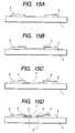
- FIG. 15A to 15D An example of manufacturing the electron-emitting device constructed as in Figs. 14A and 14B is schematically illustrated in Figs. 15A to 15D.
- a pair of electrodes 2 and 3 are first formed on a substrate 1 (Fig. 15A), followed by forming a conductive film 4 for connecting between the electrodes 2 and 3 (Fig. 15B). Then, an electric current is fed between the electrodes 2 and 3 and the so-called "a forming step" is performed for forming a second gap 5 in a part of the conductive film 4 (Fig. 15C).
- a voltage is applied between the electrodes 2 and 3 to perform the so-called “an activation step” by which a carbon film 6 is formed on a part of the substrate 1 within the area of a second gap 5 and is also formed on a part of the conductive film 4 adjacent to the second gap 5, resulting in an electron-emitting device (Fig. 15D).
- the method includes the steps of depositing a film of an organic substance such as thermosetting resin, electron beam negative resist, or polyacrylonitrile on a conductive film and carbonizing the organic substance.
- an image forming device such as a flat panel display can be constructed by combining an electron source comprised of a plurality of electron-emitting devices manufactured by the above method with an image forming member comprised of a fluorescent substance.
- the activation step and other steps are performed in addition to “the forming step” in the conventional device as described above, so that in the second gap 5 formed through the “the forming step", there is arranged a carbon film 6 made of carbon or a carbon composition having a first gap 7, which is narrower that the second gap 5. Accordingly, measures are taken to obtain excellent electron-emitting characteristics.
- the method of manufacturing the image forming apparatus using the conventional electron-emitting devices has the following problems.
- the conventional method included many additional steps in each step, for example multiple electrification steps in “the forming step” and “the activation step” and the additional step of forming an appropriate atmosphere in each step, so that process control would be complicated.
- an object of the present invention is to provide a method of manufacturing an electron-emitting device, especially permitting the simplified steps for the manufacture of an electron-emitting device and also permitting improvements in electron-emitting characteristics, a method of manufacturing an electron source, and a method of manufacturing an image forming apparatus.
- the present invention has been made as a result of extensive studies for solving the above-mentioned problems and therefore the present invention has the following configuration.
- the polymer film containing the photosensitive material is a negative-type or a positive-type photosensitive polymer film; the step of patterning using the light is performed by exposing a desired area of the negative-type photosensitive polymer film to the light and then removing an unexposed area of the negative-type photosensitive polymer film, or by exposing an area other than a desired area of the positive-type photosensitive polymer film to the light and then removing the exposed area of the positive-type photosensitive polymer film;
- the patterned polymer film is a polyimide film;
- the step of lowering the resistance of the polymer film includes the step of irradiating light on the patterned polymer film or the step of irradiating electron beam on the patterned polymer film;
- the step of lowering the resistance of the polymer film includes the step of irradiating ion beam on the patterned polymer film or the step of heating the patterned polymer film; and the step of forming a gap in the resistance-lowered film is performed by allowing
- a plurality of electron-emitting devices are manufactured in accordance with the above-mentioned method, thereby constituting one electron source.
- the electron source and an image forming apparatus constitute the image forming apparatus of the present invention.
- a polymer film including a photosensitive material is patterned using light, so that a uniform polymer films that disposed in a large area can be obtained. Therefore, the uniformity of each electron-emitting device is also increased, so that improvements in electron-emitting characteristics of such a device can be attained.
- the polymer film including the photosensitive material is patterned using light to form one having a desired shape and a desired film thickness, and the uniformed polymer film thus obtained is irradiated with light, laser beam, or the like. Therefore, the resistance of the polymer film can be uniformly and appropriately lowered.
- the steps of forming an atmosphere including an organic material, forming the polymer film on a conductive film with accuracy, and so on can be omitted, so that the manufacturing process can be simplified.
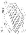
- Fig. 17 is a perspective view schematically illustrating an image forming apparatus using electron-emitting devices 102 prepared by a manufacturing method according to the present invention.
- a part of a supporting frame 72 and a part of a face plate 71 which will be described below, are removed for illustrating the inside of the image forming apparatus (an airtight container 100).
- reference numeral 1 denotes a rear plate provided as an electron source substrate on which a plurality of electron-emitting devices 102 are disposed
- 71 denotes a face plate on which an image forming member 75 is mounted
- 72 denotes a supporting frame for retaining a space between the face plate 71 and the rear plate 1 under a reduced pressure
- 101 denotes a spacer for retaining a space between the face plate 71 and the rear plate 1.
- the image forming member 75 comprises a phosphor film 74 and a conductive film 73 such as a metalback.
- Reference numerals 62 and 63 denote wirings for applying voltages on respective electron-emitting devices 102, respectively.
- Doy1 to Doyn and Dox1 to Doxm denote output wirings for connecting between a drive circuit or the like arranged on the outside of the image forming apparatus 100 and the ends of the wirings 62 and 63 guided from a decompressed space (a space surrounded by the face plate, the rear plate, and the supporting frame) of the image forming apparatus to the outside.
- FIG. 1A is a plan view
- Fig. 1B is a sectional side view of the electron-emitting device 102.
- reference numeral 1 denotes a substrate (a rear plate)
- 2 and 3 denote respective electrodes (device electrodes)
- 6' denotes an electrically conductive film containing carbon as a main ingredient (a carbon film)
- 5' denotes a gap.
- the conductive film 6' containing carbon as a main ingredient, is arranged on the substrate 1 between the electrodes 2 and 3.
- the conductive film 6' covers part of the electrodes 2 and 3 to make a definite connection with the respective electrodes 2 and 3.
- the above conductive film 6' may be alternatively referred to as "a carbon film (i.e., an electrically conductive film containing carbon as a main ingredient) having a gap in part thereof, which is responsible for making an electrical connection between a pair of electrodes".
- a pair of carbon films i.e., a pair of electrically conductive films containing carbon as a main ingredient
- electrons can be tunneling the gap 5' when a sufficient electric field is applied in the gap 5', then an electric current flows between the electrodes 2 and 3. A part of the tunnel electrons becomes emission current by means of scattering.
- the conductive film 6' does not have an electrical conductivity over the full length and full width thereof, at least a part thereof may have its own electrical conductivity. If such a conductive film 6' is made of an insulating material, electrons cannot be emitted because a sufficient electric field cannot be placed on the gap 5' even though a potential difference is placed between the electrodes 2 and 3. Thus, the conductive film 6' has an electric conductivity at least at a region between the electrode 2 (and the electrode 3) and the gap 5', allowing the gap 5' to have a sufficient electric field.
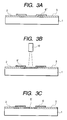
- Figs. 2A to 2D and 3A to 3C illustrate an example of the method of manufacturing an electron-emitting device according to the present invention.
- description will be made of such a method with reference to these figures as well as Figs. 1A and 1B.
- a base plate (a substrate) 1 made of glass or the like is sufficiently washed with detergent, pure water, organic solvent, and so on. Then, an electrode material is deposited on the surface of the cleaned substrate 1 by means of a vacuum deposition, a sputter deposition, or the like, followed by forming electrodes 2 and 3 on the substrate 1 using a photolithography or the like (Fig. 2A).
- the substrate 1 may be made of a glass such as a silica glass, a laminated glass in which a SiO 2 layer is laminated on a soda-lime glass, or a glass in which the amount of an alkali metal such as Na is reduced.
- the electrode material may be an oxide conductive material, which is a transparent conductive material, such as a film of tin oxide and indium oxide (ITO) if required, for example when the process of laser irradiation is performed as described later.
- oxide conductive material which is a transparent conductive material, such as a film of tin oxide and indium oxide (ITO) if required, for example when the process of laser irradiation is performed as described later.
- ITO indium oxide
- a polymer film 21 is formed on the substrate 1 on which the electrodes 2 and 3 has formed to make a connection between these electrodes 2 and 3 (Fig. 2B).
- the polymer film 21 may be a polyimide film.
- the process for preparing the polymer film is one of various methods well-known in the art including spin coating, printing, dipping, splaying, and so on.
- a polyimide precursor solution 21 containing a photosensitive material is applied on the surface of the substrate 1 by means of a spin coating method.
- a solvent for solving the polymer precursor may be selected from N-methyl-2-pyrrolidone, N,N-dimethyl acetamide, N,N-dimethyl formamide, dimethyl sulfoxide, and so on.
- n-butyl cellosolve, triethanolamine, or the like may be additionally used in combination with such a solvent.
- the substrate is pre-baked for removing the solvent.
- the pre-bake may be performed at a temperature of 100°C or less depending on the kind of the photosensitive material used.
- a photo mask 22 (Fig. 2C or Fig. 2D).
- the photo mask 22 is previously prepared to provide a polyimide film (i.e., a polymer film 6") with a predetermined pattern for making a connection between the electrodes 2 and 3.
- a polyimide film i.e., a polymer film 6
- a positive mask of the same there is shown an example of a negative mask of photosensitive polymer.
- the irradiated light may be of ultraviolet radiation, far-ultraviolet radiation, visible radiation, single wavelength rays (e.g., g-line or i-line), or the like.
- light beams previously formed into a predetermined shape may be irradiated only on a desired area.
- undesired portions i.e., areas where the light is not irradiated when the negative mask is used or areas where the light is irradiated when the positive mask is used
- a developer to obtain a polymer film 6" having a desired shape (Fig. 3A).
- the developer may be, but not limited to, a mixture of a good solvent such as N-methyl-2-pyrrolidone, N,N-dimethyl acetamide, or N,N-formamide and a poor solvent such as lower alcohol or aromatic hydrocarbon.
- a good solvent such as N-methyl-2-pyrrolidone, N,N-dimethyl acetamide, or N,N-formamide
- a poor solvent such as lower alcohol or aromatic hydrocarbon.
- the developer may be, but not limited to, an aqueous solution of tetramethylammonium hydroxide or the like may be used. After the development, the substrate 1 is rinsed to remove the developer if required.
- the electron-emitting device of the present invention is prepared using the negative mask, the area on which the polymer film 6" is to be formed can be hardened, while the undesired polymer on the remaining area can be easily removed by washing or the like.
- the negative mask is preferably used because of the following reason. That is, comparing with the positive mask, the undesired residue is unlikely found on the surface of the substrate 1 after the development especially in the case of applying the method of manufacturing the electron-emitting device of the present invention on the method of manufacturing an electron source where a plurality of wirings is used for connections of a number of the electron-emitting devices.
- a negative mask i.e., a negative photosensitive polyimide
- a positive mask i.e., a positive photosensitive polyimide
- the positive mask applied on the areas except an area where the polymer film is to be formed should be removed, so that there is a need to sufficiently irradiate light on stepped portions of the wirings, for example. Therefore, comparing with the negative mask, the residue can be easily remained after the development when the positive mask is used.
- a polyimide pattern obtained by the above development is heated at a temperature of 200°C to 400°C such that cyclopolymerization is achieved, resulting in a polyimide film.
- the polyimide used may be one prepared by converting a polyamic acid obtained from a reaction between an aromatic dianhydride such as pyromellitic dianhydride, benzophenone tetracarbonic dianhydride, biphenyl tetracarbonic dianhydride, naphthalene tetracarbonic dianhydride, or the like and an aromatic diamine compound such as phenylenediamine, diaminophenyl ether, benzophenone diamine, bis(aminophenoxy)biphenyl, 2,2'-bis(4-aminophenyl) propane, 2,2'-bis[aminophenoxy(phenyl)]propane, or the like into an imide form.
- a photosensitive material is included in such a polyamic acid solution.
- the photosensitive material included in the polyimide may be dimerizable or polymerizable C-C double bound or amino group or quaternary salts thereof, for example, (N, N-dialkyl aminoethoxy)acrylates and quaternary ammonium salts thereof, (N, N-dialkylaminoethoxy)methacrylates or quaternary ammonium salts thereof or the like, or those in which bonds are cleaved by partial breakdown with light, or polyamic acid polymerized with diamine after generating dianhydride prior to polymerization and alcohols and esters having photosensitive groups.
- the present invention is not only limited to those materials.
- a photo-polymerization initiator, a sensitizer, a copolymerization monomer, an adhesive modifier, or the like may be additionally included if required.
- the photo-polymerization initiator or the sensitizer may be one selected from benzoin ethers, benzyl ketals, acetophenone derivatives, benzophenone derivatives, xanthones, and so on.
- the copolymerization monomer may be monomaleimides, polymaleimides, or substitution products thereof. Needless to say, the present invention is not limited to these compounds.
- the aromatic polyimide is capable of easily expressing an electric conductivity by dissociating the bonding between carbon atoms and recombining thereof at a comparatively low temperature.
- the aromatic polyimide is a polymer capable of easily generating a double bond between carbon atoms. Therefore, the aromatic polyimide can be a preferable material for the above polymer film.
- the patterned polymer film 6" is subjected to "the resistance-lowering process” by which the resistance of the film 6" can be lowered.
- the resistance-lowering process allows the polymer film 6" to express the electric conductivity and converts the polymer film 6" into the film containing carbon as a main ingredient (the carbon film) 6'.
- the resistance-lowering process is performed until the sheet resistance of the polymer film 6" is lowered within the range of 10 3 ⁇ / ⁇ to 10 7 ⁇ / ⁇ .
- An example of such a process is to lower the resistance of the polymer film 6" by the application of heat.
- the reason why the resistance of the polymer film 6" is lowered may be the expression of electric conductivity by dissociating and recombining the bonding between carbon atoms in the polymer film 6".
- the "resistance-lowering process" by heat can be attained by heating the polymer constituting the polymer film 6" at a temperature equal to or more than the decomposition temperature.
- aromatic polymer described above especially aromatic polyimide, has a high heat decomposition temperature, so that it may express a high electric conductivity when it is heated at a temperature above the heat decomposition temperature, typically in the range of 700°C to 800°C or more.
- the method of manufacturing the electron-emitting device may be subjected to some type of constraints because it includes the step of entirely heating the substrate using an oven, a hot plate, or the like at a temperature enough to decompose the polymer film 6 in the view of heat resistance of other components (e.g., electrodes and substrates) that constitute the electron-emitting device.
- the substrate 1 is limited to one having a particularly high heat resistance, such as a silica glass or a ceramic substrate. Considering the application to a display panel or the like having a large area, such a substrate 1 may result in an extremely expensive product.
- the irradiation of electron beam, ion beam, or light to the polymer film 6" is performed.
- Laser beams or halogen light can be used as the light to be irradiated to the film 6".
- electron beams are irradiated from the electron beam irradiating means 10 to the polymer film 6" to lower the resistance of the polymer film 6". In this way, there is no need to use a specific substrate while lowering the resistance of the polymer film 6".
- a more preferable result may be induced based on other factors except heat, such as the decomposition and recombination of carbon atoms in the polymer film 6" by electron beams or photons may be performed in addition to the decomposition and recombination thereof by the application of heat.
- the substrate 1 on which the electrodes 2 and 3 and the polymer film 6" are formed is placed at a position under a decompression atmosphere (i.e., in a vacuum vessel), where an electron gun is equipped.
- the polymer film 6" is irradiated with electron beam from the electronic gun placed inside the vessel.
- an accelerating voltage (Vac) may be in the range of 0.5 kV to 10 kV.
- the irradiation of electron beams may be performed preferably at a current density (Id) in the range of 0.01 mA/mm 2 to 1 mA/mm 2 .
- Id current density
- the resistance between the electrodes 2 and 3 may be monitored and the irradiation of electron beams may be terminated when the desired resistance is obtained.
- the substrate 1 on which the electrodes 2 and 3 and the polymer film 6" are formed is placed on a stage and then laser beams are irradiated on the polymer film 6".
- the irradiation of laser beams is generally performed in surroundings that inhibit oxidation (combustion) of the polymer film 6".
- the irradiation may be preferably performed using a second harmonic wave (a wavelength of 532 nm) of a pulse YAG laser.
- the resistance between the electrodes 2 and 3 may be monitored and the irradiation of laser beams may be terminated when the desired resistance is obtained.
- the gap 5' can be formed by applying a voltage between the electrodes 2 and 3 (i.e., by flowing an electric current between electrodes).
- the voltage to be applied may be preferably a pulse voltage. Therefore, the application of voltage forms the gap 5' in a part of the conductive film 6'.
- the application of voltage may be performed concurrently with the above-described resistance-lowering process. That is, voltage pulses are successively applied between the electrodes 2 and 3 while irradiating energy beam (ex. electron beams, light or laser beams). Whatever the case may be, the application of voltage may be advantageously performed under a reduced pressure, preferably under an atmosphere at a pressure of 1.3 ⁇ 10 -3 Pa or less.
- the formation of the gap 5' requires a large amount of electric power.
- the progress of lowering the resistance may be adjusted.
- the resistance-lowering process may be performed over the whole area of the polymer film 6" in a uniform manner. Alternatively, it is possible to address this problem by performing the resistance-lowering process only on a part of the polymer film 6".
- the electron-emitting device of the present invention is driven in a vacuum atmosphere, it is not preferable that the insulating material is exposed in a vacuum atmosphere. Thus, it is preferable that substantially the whole surface of the polymer film 6" may be properly transformed (i.e., lowering the resistance) by the irradiation of the above-mentioned electron beams or laser beams.
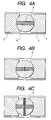
- Fig. 4 shows different views (i.e., plan views) schematically viewing the electron-emitting device of the present invention, where the resistance of a part of the polymer film 6" is lowered in the direction parallel to the surface of the substrate. More concretely, Fig. 4A is before the step of voltage application, Fig. 4B is immediately after the start of the step of voltage application, and Fig. 4C is at the time of completing the step of voltage application.
- the application of a voltage allows a current to flow through the area 6' where the resistance is lowered, forming a narrow gap 5" in the conductive film 6".
- a gap 5" is the starting point of forming the gap 5' (Fig. 4B).
- heat is applied on the periphery of the narrow gap 5".
- the area which has not been thermally decomposed becomes gradually thermally decomposed, so that the gap 5' is finally formed over the whole polymer film 6" in the direction substantially parallel to the surface of the substrate (Fig. 4C).
- the polymer film on which the process of heat decomposition is partially conducted shows good electron-emitting characteristics.
- the reason for this is not clear.
- undecomposed polymers easily move in the vicinity of the gap 5' by means of thermal diffusion. Therefore, it is assumed that a gap more appropriate for the electron emission is formed and retained and is structured so as to be less deteriorated due to driving. In such a case, it is not preferable that an insulated part where the resistance thereof is not lowered because of the above-mentioned reason is exposed on the surface. Therefore, a resistive layer (conductive layer having higher sheet-resistance than that of the reitance-lowerd film 6') having an antistatic effect may be preferably formed on the whole surface containing the device except for the gap 5'.
- the electron-emitting device obtained by the steps described above is subjected to the measurement of voltage-current characteristics using a measurement apparatus shown in Fig. 5.
- the resulting characteristics are shown in Fig. 16.
- the same reference numerals as those used in Figs. 1A and 1B denote the same structural components as those of Figs. 1A and 1B, respectively.
- Reference numeral 54 denotes an anode
- 53 denotes a high-voltage power supply
- 52 denotes an ampere meter for measuring an emission current Ie emitted from the electron-emitting device
- 51 denotes a power supply for applying a drive voltage Vf on the electron-emitting device
- 50 denotes an ampere meter for measuring a device current flowing between the electrodes 2 and 3.
- the above electron-emitting device has a threshold voltage Vth. Therefore, if a voltage which is lower than the threshold voltage Vth is placed between the electrodes 2 and 3, there is no substantial emission of electrons. However, if a voltage which is higher than the threshold voltage Vth is placed, the generation of emission current (Ie) from the device and the generation of device current (If) flowing between the electrodes 2 and 3 are initiated.
- the electron-emitting device has the above characteristics, a plurality of the electron-emitting devices can be disposed in a matrix form on the same substrate to form an electron source. Therefore, it becomes possible to perform a matrix drive by selecting the desired device and driving the selected device.
- the above "sealing step” may be preferably performed in a reduced pressure (vacuum) atmosphere or in a non-oxidative atmosphere.
- the reduced pressure (vacuum) atmosphere may be at a pressure of 10 -5 Pa or less, preferably at a pressure of 10 -6 Pa or less.
- This sealing step allows the contact portion between the face plate 71 and the supporting frame 72 and the contact portion between the supporting plate 72 and the rear plate to be airtight. Simultaneously, an airtight container (an image forming apparatus) 100 shown in Fig. 17 and having the inside kept at a high vacuum can be obtained.
- the above example is the “sealing step” performed in a reduced pressure (vacuum) atmosphere or in a non-oxidative atmosphere.
- the above “sealing step” may be performed in the air.
- an exhaust tube for exhausting air from a space between the face plate 71 and the rear plate may be additionally formed in the airtight container 100.
- the exhaust tube exhausts air from the inside of the airtight container 100 so as to become a pressure of 10 -5 Pa or less. Subsequently, the exhaust tube is closed to obtain the airtight container (the image forming apparatus) 100 with the inside thereof being kept in a high vacuum.
- the above “sealing step” is performed in a vacuum, for keeping the inside of the image forming apparatus (the airtight container) 100 in a high vacuum, it is preferable to include a step of covering the metal back 73 (the surface of the metal back facing to the rear plate 1) with a getter material between the above step (I) and step (J).
- the getter material to be used is preferably an evaporative getter (ex. Ba getter) because it simplifies the covering. Therefore, it is preferable to use barium as a getter film and to cover the metal back 73 with the getter film.
- the step of covering with the getter is performed under a reduced pressure (vacuum) atmosphere just as in the case of the above step (J).
- the spacer 101 is arranged between the face plate 71 and the rear plate 1.
- the spacer 101 is not necessarily required.
- the distance between the rear plate 1 and the face plate 71 is about several hundred micrometers, there is no need to obtain the support frame 72. It is possible to join tightly the rear plate 101 and face plate 71 with the joining member. In such a case, the joining member also supports as an alternative material of the supporting frame 72.
- step (H) of forming a gap 5' of the electron-emitting device 102
- step (I)) and the sealing step (step (J)) are performed.
- step (H) may also be performed after the sealing step (step J).
- an electron-emitting device of this example an electron-emitting device of the same type as one shown in Figs. 1A and 1B was prepared by the same method as one shown in Figs. 2A to 2D and 3A to 3C. Referring now to Figs. 1A to 3C, the method of manufacturing an electron-emitting device of this example will be described below.
- a silica glass was used as a substrate 1.
- the silica glass was washed in pure water and an organic solvent, sufficiently.
- device electrodes 2 and 3 made of platinum were formed on the substrate 1 (Fig. 2A).
- the distance L between the device electrodes 2 and 3 were 10 ⁇ m.
- the width W of the device electrode was 500 ⁇ m, while the thickness thereof was 100 nm.
- the light exposure was 100 mJ/cm 2 .
- an immersing development was performed using a mixed solvent of N-methyl-2-pyrolidone and lower alcohol.
- the substrate 1 was rinsed in isopropyl alcohol, followed by heating at 200°C for 30 minutes in the oven. Subsequently, it was baked at a temperature of up to 350°C to make it into an imide form.
- the resulting pattern image was excellent and the film thickness of the polymer film 6" was 30 nm (Fig. 3A).
- the substrate 1 formed with the electrodes 2 and 3 and the polymer film 6 on which the laser beams were irradiated was transferred.
- reference numeral 51 denotes an electric supply for applying a voltage to the device
- 50 denotes an ampere mater for measuring a device current
- 54 denotes an anode electrode for the measurement of emission current Ie to be generated from the device
- 53 denotes a high-voltage power supply for applying a voltage to the anode electrode 54
- 52 denotes an ampere mater for measuring the emission current.
- the power supply 51 and the ampere mater 50 are connected to their respective device electrodes 2 and 3.
- an anode electrode 54 is arranged above the electron-emitting device, where the anode electrode 54 is connected to the electric supply 53 and the ampere mater 52.
- the electron-emitting device and the anode electrode 54 are arranged in the vacuum device, which is equipped with necessary devices, although not shown, such as an exhausting pipe, a vacuum gauge, and the like, so that the measurement can be performed in a predetermined vacuum condition.
- the distance H between the anode electrode and the electron-emitting element was 4 mm and the pressure in the vacuum device was 1 ⁇ 10 -6 Pa.
- the electron-emitting device of the present invention was prepared.
- a voltage of 1 kV is applied on the anode electrode 54, while placing a drive voltage of 22V between the device electrodes 2 and 3 of the electron-emitting device of this example.
- the electron-emitting device of the same type as one shown in Figs. 1A and 1B was prepared by the same method as one shown in Figs. 2A to 2D and 3A to 3C.
- the formation of a polymer film used a solution of photosensitive polyimide precursor prepared in "Preparation Example 2 of photosensitive polyimide". Accordingly, referring now to Figs. 1A, 1B, 2A to 2D, and 3A to 3C, the method of manufacturing an electron-emitting device of this example will be described.
- a silica glass was used as a substrate 1.
- the silica glass was washed in purified water and an organic solvent, sufficiently.
- device electrodes 2 and 3 made of platinum were formed on the substrate 1 (Fig. 2A).
- the distance L between the device electrodes 2 and 3 was 10 ⁇ m.
- the width W of the device electrode was 500 ⁇ m, while the thickness thereof was 100 nm.
- an anode voltage of 1 kV is applied, while placing a drive voltage of 20 V between the device electrodes 2 and 3 of the electron-emitting device of this example.
- An electron-emitting device of this example is principally of the same configuration as that of the electron-emitting device described in each of Examples 1 and 2. Referring again to Figs. 1A, 1B, 2A to 2D, and 3A to 3C, a method of manufacturing an electron-emitting device of this example will be described.
- a quartz glass substrate was used as a substrate 1.
- the silica glass substrate was washed in distilled water and an organic solvent, sufficiently.
- device electrodes 2 and 3 made of ITO were formed on the substrate 1 (Fig. 2A).
- the distance L between the device electrodes 2 and 3 was 10 ⁇ m.
- the width W of the device electrode was 500 ⁇ m, while the thickness thereof was 100 nm.
- a polymer film 6" comprised of a polyimide film was prepared from a photosensitive polyimide precursor and was provided on the substrate 1 thus prepared.
- SHG a wavelength of 532 nm
- Q switch pulse Nd:YAG laser a pulse width of 100 nm, a repetition frequency of 10 kHz
- the substrate 1 was picked up and was then observed with an optical microscope. As a result, the same configuration as one shown in Fig. 4A was observed.
- an image forming apparatus 100 schematically illustrated in Fig. 16 was prepared.
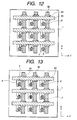
- Fig. 13 is an enlarged view schematically illustrating a part of an electron source which comprises a rear plate, a plurality of electron-emitting devices formed on the rear plate, and wirings for applying signals on the plurality of electron-emitting devices.
- reference numeral 1 denotes a rear plate
- 2, 3 denote electrodes
- 5' denotes a gap
- 6' denotes a carbon-based conductive film (a carbon film)
- 62 denotes a X directional wiring
- 63 denotes a Y directional wiring
- 64 denotes an interlayer insulting layer.
- Reference numeral 71 denotes a face plate comprised of a glass substrate on which a phosphor film 74 and a metal back 73 made of Al are laminated
- 72 denotes a supporting frame.
- a vacuum container is composed by the rear plate 1, the face plate 71, and the supporting frame 72.
- a platinum (Pt) film of 100 nm in thickness was deposited on the glass substrate 1 by a spattering method and the electrodes 2 and 3 made of the Pt film were formed using a photolithographic technique (Fig. 6).
- the distance between the electrodes 2 and 3 was 10 ⁇ m.
- a silver (Ag) paste was printed on the substrate 1 by a screen printing method and was then baked by the application of heat to form the wiring 62 in the X direction (Fig. 7).
- an insulating paste was printed on a position at an intersecting point between the wiring 62 in the X direction and the wiring 63 in the Y direction by a screen printing method, and then baked by the application of heat to form the insulating layer 64 (Fig. 8).
- the Ag paste was printed on the substrate 1 by a screen printing method and was then baked by the application of heat to form the wiring 63 in the Y direction, resulting a matrix wiring on the substrate 1 (Fig. 9).
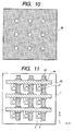
- a photosensitive polyimide precursor solution prepared in "Preparation Example 1 of photosensitive polyimide” was applied on the substrate 1 by means of a spray method so as to be extended over the electrodes 2 and 3 on the substrate 1 where the matrix wiring was formed as described above. Then, the solvent was dried in an oven. After that, the substrate 1 was subjected to a mirror projection exposure machine using an extra-high pressure mercury lamp as an light source through a mask 65 (Fig. 10) having a circular opening with 100 ⁇ m in diameter, which extends over the device electrodes in each device. After that, the substrate 1 was subjected to an immersed development using a mixture solution of N-methyl-2-pyrrolidone and lower alcohol.
- the substrate 1 was rinsed in isopropyl alcohol and was then heated in the oven at 200°C for 30 minutes, followed by baking at 350°C in a vacuum, resulting in a polymer film 6" comprised of a polyimide film in the shape of a circle having a diameter of about 100 ⁇ m and a film thickness of 30 nm (Fig. 11).
- the rear plate 1, having the electrodes 2 and 3 made of Pt, the matrix wirings 62 and 63 and the polymer film 6" comprised of the polyimide film was placed on a stage (in the air). Then, the second harmonic (SHG) of Q switch pulse Nd:YAG laser (a pulse width of 100 nm, a repetition frequency of 10 kHz, a beam diameter of 10 ⁇ m) was irradiated on the polymer film 6". At this time, the stage was moved to irradiate the polymer film 6" in the direction from the electrode 2 to the electrode 3 with a width of 10 ⁇ m. A conductive area where thermal decomposition is progressed was prepared on a part of each polymer film 6".
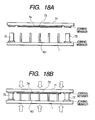
- the supporting flame 72 and a spacer 101 were adhered using a frit glass. Then, the rear plate 1 onto which the spacer 101 and the supporting frame 72 are adhered was faced to the face plate 71 (facing the surface on which the phosphor film 74 and the metal back 73 were formed with the surface on which the wirings 62, 63 were formed) (Fig. 18A). Furthermore, the frit glass was applied on the contacting portion with the supporting frame 72 on the face plate 71 in advance.
- the face plate 71 and the rear plate 1 which were opposite to each other were sealed with each other by heating and pressing at 400°C in a vacuum atmosphere of 10 -6 Pa. As a result of this step, a sealed container retaining a high vacuum in the inside was obtained.
- phosphor film 74 phosphors of the three primary colors (RGB) were arranged in a strip shape.
- the polymer film including a photosensitive material is subjected to patterning using light so that it can be prepared as one having a large area and a uniform shape.
- the resistance of the polymer film can be lowered to form a gap, so that the improvement in electron-emitting characteristics can be attained as the uniformity of each device can be increased.
- the electron source in which the plurality of electron-emitting devices or the image forming apparatus can be display a clear image with an excellent quality in a large area for a long time.
Landscapes
- Engineering & Computer Science (AREA)
- Manufacturing & Machinery (AREA)
- Cold Cathode And The Manufacture (AREA)
Applications Claiming Priority (4)
| Application Number | Priority Date | Filing Date | Title |
|---|---|---|---|
| JP2001313540 | 2001-10-11 | ||
| JP2001313540 | 2001-10-11 | ||
| JP2002259614 | 2002-09-05 | ||
| JP2002259614A JP3902995B2 (ja) | 2001-10-11 | 2002-09-05 | 電子放出素子、電子源及び画像形成装置の製造方法 |
Publications (2)
| Publication Number | Publication Date |
|---|---|
| EP1302968A2 true EP1302968A2 (fr) | 2003-04-16 |
| EP1302968A3 EP1302968A3 (fr) | 2007-07-25 |
Family
ID=26623844
Family Applications (1)
| Application Number | Title | Priority Date | Filing Date |
|---|---|---|---|
| EP02022696A Withdrawn EP1302968A3 (fr) | 2001-10-11 | 2002-10-10 | Procédé de fabrication d'un dispositif émetteur d'électrons, d'une source d'électrons et d'un appareil de formation d'images |
Country Status (5)
| Country | Link |
|---|---|
| US (1) | US6988922B2 (fr) |
| EP (1) | EP1302968A3 (fr) |
| JP (1) | JP3902995B2 (fr) |
| KR (1) | KR100535964B1 (fr) |
| CN (1) | CN1278355C (fr) |
Cited By (1)
| Publication number | Priority date | Publication date | Assignee | Title |
|---|---|---|---|---|
| EP2031628A1 (fr) * | 2007-08-31 | 2009-03-04 | Canon Kabushiki Kaisha | Appareil à émission de champ et procedè de sa fabrication |
Families Citing this family (15)
| Publication number | Priority date | Publication date | Assignee | Title |
|---|---|---|---|---|
| JP3634805B2 (ja) * | 2001-02-27 | 2005-03-30 | キヤノン株式会社 | 画像形成装置の製造方法 |
| JP3634828B2 (ja) * | 2001-08-09 | 2005-03-30 | キヤノン株式会社 | 電子源の製造方法及び画像表示装置の製造方法 |
| JP3884979B2 (ja) * | 2002-02-28 | 2007-02-21 | キヤノン株式会社 | 電子源ならびに画像形成装置の製造方法 |
| JP3902964B2 (ja) * | 2002-02-28 | 2007-04-11 | キヤノン株式会社 | 電子源の製造方法 |
| JP3634850B2 (ja) * | 2002-02-28 | 2005-03-30 | キヤノン株式会社 | 電子放出素子、電子源および画像形成装置の製造方法 |
| JP3884980B2 (ja) * | 2002-02-28 | 2007-02-21 | キヤノン株式会社 | 電子源及び該電子源を用いた画像形成装置の製造方法 |
| JP3634852B2 (ja) * | 2002-02-28 | 2005-03-30 | キヤノン株式会社 | 電子放出素子、電子源及び画像表示装置の製造方法 |
| JP3619240B2 (ja) * | 2002-09-26 | 2005-02-09 | キヤノン株式会社 | 電子放出素子の製造方法及びディスプレイの製造方法 |
| JP3944155B2 (ja) | 2003-12-01 | 2007-07-11 | キヤノン株式会社 | 電子放出素子、電子源及び画像表示装置の製造方法 |
| JP4352880B2 (ja) * | 2003-12-02 | 2009-10-28 | セイコーエプソン株式会社 | 洗浄方法および洗浄装置 |
| JP3935478B2 (ja) * | 2004-06-17 | 2007-06-20 | キヤノン株式会社 | 電子放出素子の製造方法およびそれを用いた電子源並びに画像表示装置の製造方法および該画像表示装置を用いた情報表示再生装置 |
| JP3935479B2 (ja) * | 2004-06-23 | 2007-06-20 | キヤノン株式会社 | カーボンファイバーの製造方法及びそれを使用した電子放出素子の製造方法、電子デバイスの製造方法、画像表示装置の製造方法および、該画像表示装置を用いた情報表示再生装置 |
| KR100752509B1 (ko) * | 2005-12-30 | 2007-08-27 | 엘지.필립스 엘시디 주식회사 | 전자 방출 소자 및 그의 제조 방법 및 그를 이용한 전자방출 표시장치 및 그의 제조 방법 |
| JP2009037757A (ja) * | 2007-07-31 | 2009-02-19 | Canon Inc | 導電性薄膜、電子放出素子及び画像表示装置 |
| JP2009043568A (ja) * | 2007-08-09 | 2009-02-26 | Canon Inc | 電子放出素子及び画像表示装置 |
Citations (6)
| Publication number | Priority date | Publication date | Assignee | Title |
|---|---|---|---|---|
| JPH0765708A (ja) * | 1993-08-25 | 1995-03-10 | Canon Inc | 電子放出素子並びに画像形成装置の製造方法 |
| EP0700064A1 (fr) | 1994-08-01 | 1996-03-06 | Canon Kabushiki Kaisha | Matière pour former un film électroconducteur, méthode pour former un film électroconducteur en faisant utilisation et méthode de fabrication d'un dispositif émetteur d'électrons, source d'électrons et dispositif de formation d'images |
| JPH09237571A (ja) | 1995-12-12 | 1997-09-09 | Canon Inc | 電子放出素子の製造方法、及び、該製造方法を用いた電子源及び画像形成装置の製造方法、並びに、これらに用いられる製造装置 |
| JPH11233005A (ja) * | 1998-02-16 | 1999-08-27 | Canon Inc | 電子源、画像形成装置及びこれらの製造方法、製造装置 |
| JPH11283493A (ja) * | 1998-03-30 | 1999-10-15 | Canon Inc | 電子放出素子、電子源、画像形成装置及びそれらの製造方法 |
| EP0986085A2 (fr) * | 1998-09-07 | 2000-03-15 | Canon Kabushiki Kaisha | Procédé de fabrication d'une cathode,d' une source d'électrons et d'un dispositif de formation d'image |
Family Cites Families (29)
| Publication number | Priority date | Publication date | Assignee | Title |
|---|---|---|---|---|
| US117670A (en) * | 1871-08-01 | Improvement in hand corn-huskers | ||
| US161942A (en) * | 1875-04-13 | Improvement in fastenings for tool-handles | ||
| US160180A (en) * | 1875-02-23 | Improvement in fire-chambers for puddling and other furnaces | ||
| US162464A (en) * | 1875-04-27 | Improvement in grain-car doors | ||
| US39767A (en) * | 1863-09-01 | Improvement in cotton-gins | ||
| US162465A (en) * | 1875-04-27 | Improvement in automatic air-escapes for railway air-brakes | ||
| JPH0765704A (ja) | 1993-08-30 | 1995-03-10 | Canon Inc | 電子放出素子および画像形成装置 |
| JP3320215B2 (ja) | 1994-08-11 | 2002-09-03 | キヤノン株式会社 | 電子放出素子、電子源及び画像形成装置 |
| JP2903295B2 (ja) | 1994-08-29 | 1999-06-07 | キヤノン株式会社 | 電子放出素子、それを用いた電子源並びに画像形成装置と、それらの製造方法 |
| KR100229231B1 (ko) * | 1995-04-04 | 1999-11-01 | 미다라이 후지오 | 전자 방출 소자 형성용 금속 함유 조성물, 및 전자방출소자,전자원및화상형성장치의제조방법 |
| JPH08329827A (ja) * | 1995-05-30 | 1996-12-13 | Canon Inc | 電子放出素子、それを用いた電子源、画像形成装置 |
| JP3217950B2 (ja) * | 1995-10-11 | 2001-10-15 | キヤノン株式会社 | 電子放出素子、電子源、表示素子及び画像形成装置の製造方法 |
| JPH09161666A (ja) | 1995-12-13 | 1997-06-20 | Dainippon Printing Co Ltd | 電子放出素子の製造方法 |
| DE69719839T2 (de) * | 1996-04-26 | 2003-11-13 | Canon K.K., Tokio/Tokyo | Verfahren zur Herstellung einer Elektronen emittierenden Vorrichtung, Elektronenquelle und diese Quelle verwendendes Bilderzeugungsgerät |
| US6124914A (en) * | 1996-05-10 | 2000-09-26 | International Business Machines Corporation | Method an apparatus for forming an alignment pattern on a surface using a particle beam useful for a liquid crystal |
| JPH1055751A (ja) * | 1996-08-08 | 1998-02-24 | Canon Inc | 電子放出素子、電子源、画像形成装置及びそれらの製造方法 |
| TW565745B (en) * | 1997-10-07 | 2003-12-11 | Ibm | Compositions of matter, resist structures including a layer of electrically conductive polymer having controlled pH and methods of fabrication thereof |
| JPH11120901A (ja) | 1997-10-14 | 1999-04-30 | Japan Atom Energy Res Inst | 放射線による電界放出型冷陰極材料の作製方法 |
| JP2000082384A (ja) * | 1998-09-08 | 2000-03-21 | Canon Inc | 電子放出素子、電子源及び画像形成装置並びに電子放出素子の製造方法 |
| US6492769B1 (en) * | 1998-12-25 | 2002-12-10 | Canon Kabushiki Kaisha | Electron emitting device, electron source, image forming apparatus and producing methods of them |
| JP3323847B2 (ja) | 1999-02-22 | 2002-09-09 | キヤノン株式会社 | 電子放出素子、電子源および画像形成装置の製造方法 |
| KR100498739B1 (ko) | 2000-09-01 | 2005-07-01 | 캐논 가부시끼가이샤 | 전자방출소자, 전자원 및 화상형성장치의 제조방법 |
| JP3634805B2 (ja) | 2001-02-27 | 2005-03-30 | キヤノン株式会社 | 画像形成装置の製造方法 |
| JP3634828B2 (ja) | 2001-08-09 | 2005-03-30 | キヤノン株式会社 | 電子源の製造方法及び画像表示装置の製造方法 |
| JP3902964B2 (ja) | 2002-02-28 | 2007-04-11 | キヤノン株式会社 | 電子源の製造方法 |
| JP3634852B2 (ja) | 2002-02-28 | 2005-03-30 | キヤノン株式会社 | 電子放出素子、電子源及び画像表示装置の製造方法 |
| JP3884980B2 (ja) | 2002-02-28 | 2007-02-21 | キヤノン株式会社 | 電子源及び該電子源を用いた画像形成装置の製造方法 |
| JP3634850B2 (ja) | 2002-02-28 | 2005-03-30 | キヤノン株式会社 | 電子放出素子、電子源および画像形成装置の製造方法 |
| JP3884979B2 (ja) | 2002-02-28 | 2007-02-21 | キヤノン株式会社 | 電子源ならびに画像形成装置の製造方法 |
-
2002
- 2002-09-05 JP JP2002259614A patent/JP3902995B2/ja not_active Expired - Fee Related
- 2002-10-01 US US10260557A patent/US6988922B2/en not_active Expired - Fee Related
- 2002-10-10 KR KR10-2002-0061633A patent/KR100535964B1/ko not_active Expired - Fee Related
- 2002-10-10 EP EP02022696A patent/EP1302968A3/fr not_active Withdrawn
- 2002-10-11 CN CNB021468095A patent/CN1278355C/zh not_active Expired - Fee Related
Patent Citations (7)
| Publication number | Priority date | Publication date | Assignee | Title |
|---|---|---|---|---|
| JPH0765708A (ja) * | 1993-08-25 | 1995-03-10 | Canon Inc | 電子放出素子並びに画像形成装置の製造方法 |
| EP0700064A1 (fr) | 1994-08-01 | 1996-03-06 | Canon Kabushiki Kaisha | Matière pour former un film électroconducteur, méthode pour former un film électroconducteur en faisant utilisation et méthode de fabrication d'un dispositif émetteur d'électrons, source d'électrons et dispositif de formation d'images |
| JPH09237571A (ja) | 1995-12-12 | 1997-09-09 | Canon Inc | 電子放出素子の製造方法、及び、該製造方法を用いた電子源及び画像形成装置の製造方法、並びに、これらに用いられる製造装置 |
| JPH11233005A (ja) * | 1998-02-16 | 1999-08-27 | Canon Inc | 電子源、画像形成装置及びこれらの製造方法、製造装置 |
| JPH11283493A (ja) * | 1998-03-30 | 1999-10-15 | Canon Inc | 電子放出素子、電子源、画像形成装置及びそれらの製造方法 |
| EP0986085A2 (fr) * | 1998-09-07 | 2000-03-15 | Canon Kabushiki Kaisha | Procédé de fabrication d'une cathode,d' une source d'électrons et d'un dispositif de formation d'image |
| JP2000299053A (ja) * | 1998-09-07 | 2000-10-24 | Canon Inc | 電子放出素子、電子源、及び画像形成装置の製造方法 |
Non-Patent Citations (1)
| Title |
|---|
| HOU H ET AL: "Ester-type precursor of polyimide and photosensitivity", EUROPEAN POLYMER JOURNAL, PERGAMON PRESS LTD. OXFORD, GB, vol. 35, no. 11, 1 November 1999 (1999-11-01), pages 1993 - 2000, XP004182906, ISSN: 0014-3057, DOI: 10.1016/S0014-3057(98)00290-0 * |
Cited By (2)
| Publication number | Priority date | Publication date | Assignee | Title |
|---|---|---|---|---|
| EP2031628A1 (fr) * | 2007-08-31 | 2009-03-04 | Canon Kabushiki Kaisha | Appareil à émission de champ et procedè de sa fabrication |
| US7837529B2 (en) | 2007-08-31 | 2010-11-23 | Canon Kabushiki Kaisha | Electron-emitting device and manufacturing method thereof |
Also Published As
| Publication number | Publication date |
|---|---|
| JP2003187691A (ja) | 2003-07-04 |
| KR20030030933A (ko) | 2003-04-18 |
| US20030073371A1 (en) | 2003-04-17 |
| CN1412808A (zh) | 2003-04-23 |
| US6988922B2 (en) | 2006-01-24 |
| EP1302968A3 (fr) | 2007-07-25 |
| KR100535964B1 (ko) | 2005-12-09 |
| JP3902995B2 (ja) | 2007-04-11 |
| CN1278355C (zh) | 2006-10-04 |
Similar Documents
| Publication | Publication Date | Title |
|---|---|---|
| EP1302968A2 (fr) | Procédé de fabrication d'un dispositif émetteur d'électrons, d'une source d'électrons et d'un appareil de formation d'images | |
| US6992428B2 (en) | Electron emitting device, electron source and image display device and methods of manufacturing these devices | |
| US6896571B2 (en) | Methods of manufacturing electron-emitting device, electron source, and image display apparatus | |
| US7335081B2 (en) | Method for manufacturing image-forming apparatus involving changing a polymer film into an electroconductive film | |
| JP3634805B2 (ja) | 画像形成装置の製造方法 | |
| US6653232B2 (en) | Method of manufacturing member pattern and method of manufacturing wiring, circuit substrate, electron source, and image-forming apparatus | |
| JP2003323845A (ja) | 電子放出素子、電子源および画像形成装置の製造方法 | |
| JP3884979B2 (ja) | 電子源ならびに画像形成装置の製造方法 | |
| JP3902964B2 (ja) | 電子源の製造方法 | |
| TW200941534A (en) | Cathode assembly containing an ultraviolet light-blocking dielectric layer | |
| JP2003288837A (ja) | 電子放出素子の製造方法 | |
| JPH0765708A (ja) | 電子放出素子並びに画像形成装置の製造方法 | |
| JP2003288838A (ja) | 電子放出素子、電子源及び画像形成装置の製造方法 | |
| JP2003197091A (ja) | 電子放出素子、電子源及び画像形成装置の製造方法 | |
| KR100774222B1 (ko) | 중성빔을 이용한 cnt 전계방출 표시소자의 제조방법 | |
| JP3634780B2 (ja) | 電子放出素子、電子源、および画像形成装置の製造方法 | |
| JP3740488B2 (ja) | 電子放出素子の製造方法 | |
| JP2933855B2 (ja) | 電子放出素子及びそれを用いた電子線発生装置並びに画像形成装置の製造方法 | |
| JP2003007206A (ja) | 画像形成装置の製造方法 | |
| JP2005268167A (ja) | 電子放出素子、電子源および画像形成装置の製造方法 | |
| JP2002075169A (ja) | 電子放出素子、電子源、および画像形成装置、並びにそれらの製造方法 | |
| JP2003257307A (ja) | 電子源および画像形成装置の製造方法 | |
| JPH07302966A (ja) | 配線基板修正装置、及び同装置を用いる配線基板修正方法 |
Legal Events
| Date | Code | Title | Description |
|---|---|---|---|
| PUAI | Public reference made under article 153(3) epc to a published international application that has entered the european phase |
Free format text: ORIGINAL CODE: 0009012 |
|
| AK | Designated contracting states |
Designated state(s): AT BE BG CH CY CZ DE DK EE ES FI FR GB GR IE IT LI LU MC NL PT SE SK TR |
|
| AX | Request for extension of the european patent |
Extension state: AL LT LV MK RO SI |
|
| PUAL | Search report despatched |
Free format text: ORIGINAL CODE: 0009013 |
|
| AK | Designated contracting states |
Kind code of ref document: A3 Designated state(s): AT BE BG CH CY CZ DE DK EE ES FI FR GB GR IE IT LI LU MC NL PT SE SK TR |
|
| AX | Request for extension of the european patent |
Extension state: AL LT LV MK RO SI |
|
| 17P | Request for examination filed |
Effective date: 20080125 |
|
| AKX | Designation fees paid |
Designated state(s): DE FR GB IT NL |
|
| 17Q | First examination report despatched |
Effective date: 20080424 |
|
| STAA | Information on the status of an ep patent application or granted ep patent |
Free format text: STATUS: THE APPLICATION HAS BEEN WITHDRAWN |
|
| 18W | Application withdrawn |
Effective date: 20110830 |