EP1387415A2 - Supraleitende integrierte Schaltung und deren Herstellungsverfahren - Google Patents
Supraleitende integrierte Schaltung und deren Herstellungsverfahren Download PDFInfo
- Publication number
- EP1387415A2 EP1387415A2 EP03254775A EP03254775A EP1387415A2 EP 1387415 A2 EP1387415 A2 EP 1387415A2 EP 03254775 A EP03254775 A EP 03254775A EP 03254775 A EP03254775 A EP 03254775A EP 1387415 A2 EP1387415 A2 EP 1387415A2
- Authority
- EP
- European Patent Office
- Prior art keywords
- superconducting
- substrate
- electrode
- insulating
- integrated circuit
- Prior art date
- Legal status (The legal status is an assumption and is not a legal conclusion. Google has not performed a legal analysis and makes no representation as to the accuracy of the status listed.)
- Granted
Links
Images


Classifications
-
- H—ELECTRICITY
- H10—SEMICONDUCTOR DEVICES; ELECTRIC SOLID-STATE DEVICES NOT OTHERWISE PROVIDED FOR
- H10N—ELECTRIC SOLID-STATE DEVICES NOT OTHERWISE PROVIDED FOR
- H10N60/00—Superconducting devices
- H10N60/01—Manufacture or treatment
- H10N60/0912—Manufacture or treatment of Josephson-effect devices
-
- H—ELECTRICITY
- H10—SEMICONDUCTOR DEVICES; ELECTRIC SOLID-STATE DEVICES NOT OTHERWISE PROVIDED FOR
- H10N—ELECTRIC SOLID-STATE DEVICES NOT OTHERWISE PROVIDED FOR
- H10N60/00—Superconducting devices
- H10N60/10—Junction-based devices
- H10N60/12—Josephson-effect devices
-
- H—ELECTRICITY
- H10—SEMICONDUCTOR DEVICES; ELECTRIC SOLID-STATE DEVICES NOT OTHERWISE PROVIDED FOR
- H10N—ELECTRIC SOLID-STATE DEVICES NOT OTHERWISE PROVIDED FOR
- H10N69/00—Integrated devices, or assemblies of multiple devices, comprising at least one superconducting element covered by group H10N60/00
Definitions
- This invention relates to a superconducting integrated circuit that has included superconducting components, such as superconducting tunnel junction components and microbridge components, and to a method for the fabrication thereof.
- a silicon oxide film or silicon nitride film has been used as the material for an insulating interlayer film intended to effect insulation between an upper electrode and a lower electrode.
- the insulation characteristics and dielectric characteristics of the insulating film have an effect on the signal transmission characteristics of the wiring and on the electric characteristics of the superconducting tunnel junction device as well.
- the changes in the characteristic properties of the junction component have a great effect as well on the operation characteristics of the superconducting integrated circuit and, therefore, have posed an important problem to be solved.
- the material that is used for the insulating interlayer film is expected to excel in the good insulating characteristics and to show a low dielectric constant.
- a material which is capable of fully satisfying these conditions and is as well applicable to the fabrication of a superconducting tunnel junction device has not been reported until now.
- an insulating interlayer film that comprises depositing an insulating film on the entire surface of a substrate by the technique of sputtering or the technique of evaporation using vacuum equipment, then patterning the insulating film by means of a photo resist and forming via holes in the insulating film by the technique of dry etching, and a method of forming an insulating interlayer film that comprises applying a photo resist to a substrate, patterning the applied layer of photo resist, depositing an insulating film on the patterned layer of photo resist by the technique of sputtering or the technique of evaporation using vacuum equipment and separating unnecessary layers by the lift-off technique.
- These methods invariably necessitate use of highly expensive vacuum equipment and encounter difficulty in ensuring reliability of the formation of via holes because they entail large numbers of steps.
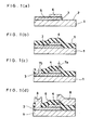
- Fig. 4 depicts a process for forming an insulating interlayer film that comprises depositing an insulating film, applying a photo resist to the entire surface of a substrate, patterning the layer of photo resist by the lithographic technique and forming via holes in the layers by the dry etching technique.
- a protective layer 2 against dry etching is formed on a substrate 1
- a tunnel junction having a structure of upper electrode 4/tunnel barrier 5/lower electrode 3 is deposited by the sputtering technique, then a resist pattern for the lower electrode and a resist pattern for the upper electrode are formed by the photolithographic technique, and a tunnel junction component and a lower wiring layer are respectively worked out by dry etching, as illustrated in Fig. 4(a).
- an insulating layer 21 of a silicon dioxide film, silicon oxide film or silicon nitride film is deposited on the entire surface of the substrate 1 by the sputtering technique or the evaporation technique without heating the substrate for the purpose of insulating the upper and lower electrodes 4 and 3, as illustrated in Fig. 4(b).
- the superconducting tunnel junction component when heated to a temperature of higher than 150°C, induces deterioration of the electrical properties, it is a general rule to avoid heating the substrate in the fabrication process.
- a photo resist 22 is applied onto the entire surface of the insulating film on the substrate 1, as illustrated in Fig. 4(c).
- photo resist patterns 23a and 23b which are intended to be used for forming via holes in the insulating layer to get electrical contacts with the upper and lower electrodes, are formed by the use of the photolithoaraphic technique, as illustrated in Fig 4(d).
- via holes 24a and 24b respectively reaching the electrodes 3 and 4 are formed by the technique of dry etching using vacuum equipment, as illustrated in Fig. 4(e)
- a wiring electrode layer is deposited over the entire surface of the substrate by the sputtering technique, then photo resist patterns to be used for wiring are formed by the photolithographic technique, and a wiring 8 is formed by dry etching to complete a superconducting tunnel device, as illustrated in Fig. 4(g).
- Fig. 5 depicts a process which comprises applying a photo resist to the entire surface of a substrate, imparting shapes of prospective via holes to the applied layer of the photo resist by the lithographic technique, then depositing an insulating film, and forming an insulating interlayer film by the lift-off technique.
- a protective layer 2 against dry etching is formed on a substrate 1, a tunnel junction having the structure of upper electrode 4/tunnel barrier 5/lower electrode 3 is deposited thereon, then a lower electrode pattern and an upper electrode pattern are formed by the photolithographic technique, and a tunnel junction component and a lower wiring layer are formed by dry etching, as illustrated in Fig. 5(a).
- a photo resist 22 is subsequently applied to the entire surface of the substrate 1, as illustrated in Fig. 5(b).
- the photo resist is removed from the applied layer of photo resist excepting the positions at which the via holes to get electrical contacts with the upper electrode 4 and the lower electrode 3 are expected to be formed by the use of the photolithographic technique to form the photo resist patterns 22a and 22b in the shapes of the prospective via holes, as illustrated in Fig. 5(c).
- an insulating layer 21, such as of a silicon dioxide film, silicon oxide film or silicon nitride film is deposited by the sputtering technique or the evaporation technique on the entire surface of the substrate 1 with the object of insulating the upper and lower electrodes, as illustrated in Fig. 5(d).
- the photo-resist patterns 22a and 22b are removed by the lift-off technique to complete an insulating interlayer film, as illustrated in Fig. 5(e).
- a wiring electrode layer is deposited on the entire surface of the insulating interlayer film by the sputtering technique, then the photo resist pattern to be used for wiring is formed by the photolithographic technique, and a wiring layer is worked out by dry etching to form a wire 8 to complete a superconducting tunnel component, as illustrated in Fig. 5(f).
- the insulating characteristics and the dielectric characteristics thereof may affect even the characteristic properties of the superconducting tunnel junction device. If the insulating film exhibits interior insulating characteristics and entails the occurrence of a leak current, for example, these defects will manifest themselves in a form superposed on the subgap leak property of a junction component. Thus, the changes in the characteristic properties of the junction component greatly affect the operation characteristics of the superconducting integrated circuit.
- the low-temperature-formed silicon oxide film and silicon nitride film that have been used as the materials for the conventional insulating films have not been fully satisfactory.
- the silicon oxide film contains oxygen, it has proved to be an unfavorable material for the niobium superconductor that tends to induce deterioration of the superconducting property by diffusion of oxygen.
- the formation of via holes in the insulating layer is implemented by dry etching, the wiring layer and the resistor layer which are exposed after the formation of via holes suffer loss of thickness due to dry etching and sustain damage of dry etching and consequently pose a serious hindrance to the formation of proper electrical contacts.
- the insulating layer of the signal line is preferably made of a material having a low dielectric constant because the signal transmission speed through this line increases in proportion as the dielectric constant of the insulating interlayer film decreases.
- An object of this invention is to provide a superconducting integrated circuit which permits the technique for forming an insulating interlayer film to be simplified because of a marked decrease in the number of steps as compared with the conventional technique, enjoys an enhanced reliability of the wiring, and enables the yield of device to be exalted and to provide a method for the mass production thereof
- Another object of this invention is to provide a superconducting integrated circuit which permits an insulating film to be deposited by a simple and convenient method of application without using vacuum equipment, allows a decrease in the number of steps of process by forming via holes exclusively by the lithographic technique, and consequently enjoys an enhanced reliability of the process for the formation of via holes.
- the superconducting integrated circuit contemplated by this invention comprises a substrate, a multilayer structure formed on the substrate and composed of a lower superconducting electrode, a tunnel barrier and an upper superconducting electrode sequentially joined together upward in the order mentioned, and an insulating layer perforated to form via holes to get electrical contacts with the lower electrode and the upper electrode, the insulating layer being formed of a high-resolution, photosensitive, solvent-soluble, organic insulating material.
- the method for the production of superconducting integrated circuit contemplated by this invention comprises depositing on a substrate a multiplayer of a lower superconducting electrode, a tunnel harrier and an upper superconducting electrode sequentially deposited upward in the order mentioned, applying a high-resolution, photosensitive, solvent-soluble, organic insulating material to a front surface of the substrate inclusive of the multilayer, forming via holes in the insulating material by a lithographic technique at prospective positions to get electrical contacts with the upper electrode and the lower electrode, and laying wirings for connecting the upper electrode and the lower electrode through the via holes
- a photosensitive solvent-soluble polyimide can be used advantageously.
- the method for the production further comprises disposing a resistor additionally on the substrate before applying the insulating material, and perforating the insulating layer to form a via hole to get electrical contacts with the resistor.
- the superconducting integrated circuit of this invention owing to the use of a photosensitive organic film having high-resolution characteristics of the level of microns to submicrons as an insulating film, is enabled to attain the formation of via holes in the insulating layer exclusively by the lithographic technique
- the method for producing this integrated circuit is simplified through a marked decrease in the number of steps of process as compared with the conventional technique for the formation of the insulating interlayer film.
- a protective layer 2 of MgO film against dry etching is formed on a substrate 1.
- a tunnel junction layer having a multilayer structure of Nb upper electrode 4/AlO x tunnel barrier 5/Nb lower electrode 3 is deposited thereon, then a resist pattern for the lower electrode and a resist pattern for the upper electrode are formed by the photolithographic technique.
- a tunnel junction layer is defined by dry etching through these resist patterns, as illustrated in Fig. 1(a).
- a high-resolution, photosensitive, solvent-soluble, organic material such as a photosensitive solvent-soluble block-copolyimide
- a high-resolution, photosensitive, solvent-soluble, organic material such as a photosensitive solvent-soluble block-copolyimide
- the application on this occasion can be done easily and conveniently by spin coating or screen-printing without using vacuum equipment.
- the thickness of the insulating film can be controlled in a very wide range, depending on the concentration and the molecular weight of the photosensitive, solvent-soluble, organic insulating material.
- the insulating film consequently formed is dried in a convection oven at a temperature of from 90 °C to 100 °C. As a result, the solvent in the film is reduced and the photosensitive characteristics are stabilized.
- Via holes 7a and 7b to be used to get electrical contacts with the upper and lower electrodes 4 and 3 are then formed by the photolithographic technique in the insulating film using a high-resolution, photosensitive, organic insulating material 6, as illustrated in Fig. 1(c).
- the high-resolution, photosensitive, insulating material such 25 a photosensitive block-copolyimide, is exposed to the ultraviolet light through a photo mask having the via-hole patterns incised therein in advance.
- the exposed insulating film is immersed in an alkali solution, such as a mixed solution composed of N-methyl-2-pyrrolidone, amino ethanol and water, to develop the relevant patterns by dissolving the exposed portions of the insulating material.
- the substrate 1 is heated to vaporize the solvent and the photosensitive material in the high-resolution, photosensitive, insulating material and complete the via holes 7a and 7b.
- the characteristic properties of the superconducting tunnel junction device should be retained at high grade.
- the heating temperature should remain at a level as low as possible.
- the heating temperature can be kept in a range of from 120 °C to 150°C and the high-grade characteristic properties can be retained. The preceding procedure completes an insulating interlayer film.
- a wiring electrode layer is deposited on the entire surface of the substrate by the sputtering technique, then a photo resist pattern for the wiring is formed by the photolithographic technique.
- the wiring layer is worked out by dry etching to give rise to a wiring 8, as illustrated in Fig. 1(d).
- the superconducting tunnel junction device in the preceding embodiment has been depicted as using a photosensitive, solvent-soluble, insulating layer for the peripheral insulation thereof, a photosensitive solvent-soluble insulating layer can be used as well for the insulation between the superconducting ground plane layer and the lower superconducting electrode layer and for the insulation between the superconducting wiring layer and the second superconducting wiring layer (control wiring layer).
- all the insulating layers in the superconducting integrated circuit can be photosensitive, solvent-soluble insulating layers.
- the superconducting tunnel junction device which used electrodes formed of a Nb superconductor experimentally fabricated in accordance with the method of this invention was found to exhibit junction characteristics which compare favorably with the top data obtained in the use of the conventional silicon dioxide film for insulating layers and which feature very small subgap leakage.
- the Vm value of the device at the voltage of 2 mV that serves as the index of device quality was 90 mV
- Fig. 2 depicts an example of the formation of a superconducting integrated circuit inclusive of a superconducting tunnel junction and a resistor as the second embodiment of this invention.
- a protective layer 2, such as of MgO, against dry etching is deposited by the evaporation or sputtering technique on a substrate 1, then a Nb lower electrode 3, an AlO x tunnel barrier 5 and a Nb upper electrode 4 are continuously formed by the sputtering technique, the lower electrode 3 and the upper electrode 4 are defined by dry etching through a resist pattern for the lower electrode and a resist pattern for the upper electrode, further a Pd resistor layer is deposited by the evaporation technique through a resist pattern for the resistor, and thereafter a fine resistor 11 is formed by the lift-off technique, as illustrated in Fig. 2(a) Incidentally, during the course of the dry etching, the etching ceases proceeding at the surfaces of the tunnel barrier 5 and the protective layer 2.
- a protective layer 2 such as of MgO
- a high-resolution, solvent-soluble, photosensitive, organic material 6 is applied to the entire surface of the substrate I, as illustrated in Fig. 2(b), and the applied layer consequently formed is pre-baked similarly at a temperature of from 90 °C to 100 °C.
- the patterns of a contact hole 7c for the resistor, a contact hole 7b for the lower electrode and a contact hole 7a for the upper electrode are exposed to ultraviolet light, and the exposed patterns are developed with an alkali and then post-baked to give rise to the respective holes, as illustrated in Fig. 2(c).
- the AlO x tunnel barrier on the lower electrode is inevitably etched by an alkali developing solution.
- a Nb wiring layer is deposited on the entire surface, and the deposited layers are dry etched through a resist pattern for wiring to give rise to a wiring 8, as illustrated in Fig 2(d).
- the present embodiment is compared with the conventional method for fabricating a superconducting integrated circuit using an SiO 2 film for insulating layers.
- the contact holes are formed by only lithographic process with ultraviolet light.
- the contact holes are formed by dry etching through resist patterns for contact holes on the SiO 2 film. Therefore, a resistor layer and an upper electrode are exposed to the etching plasma.
- the conventional method is required to prepare two contact patterns, one for the resistor and the other for the upper electrode, and individually optimize the dry etching conditions for the two contact patterns.
- the margin for the over-etching further etching for eliminating the residue of etching
- the present invention is capable of providing a fabrication method that, owing to the use of a photosensitive organic material, features exceptional convenience and high reliability as well.
- Fig. 3 depicts a method for producing a superconducting integrated circuit inclusive of a ground plane, a wire-bonding pad, a superconducting tunnel junction and a resistor as the third embodiment of this invention.
- a protective layer 2, such as of MgO, against dry etching is deposited on a substrate 1 by the evaporation or sputtering technique and then a Nb ground plane 9 is formed thereon by the sputtering technique, as illustrated in Fig. 3(a).
- a SiO 2 insulating interlayer layer 10 is formed as by the sputtering technique, a protective layer 2a against dry etching is deposited by the evaporation or sputtering technique, then a Nb lower electrode 3, an AlO x tunnel barrier 5 and a Nb upper electrode 4 are continuously formed by the sputtering technique, the lower electrode 4 and the upper electrode 5 are defined by dry etching respectively through a resist pattern for the lower electrode and a resist pattern for the upper electrode, further a Pd resistor layer is deposited by the evaporation technique through a resist pattern for the resistor, and a fine resistor 11 is formed by the lift-off technique.
- the etching ceases proceeding at the surfaces of the tunnel barrier and the protective layer.
- the insulating interlayer layer 10 is removed by dry etching prior to the formation of a junction tri-layer (a Nb lower electrode 3, an AlO x tunnel barrier 5 and a Nb upper electrode 4)
- a separating part 13 separates electrically the ground plane 9 and the wirc-bonding pads 12.
- a groove is formed by dry etching and then refilled with SiO or poly Si.
- a high-resolution, solvent-soluble, photosensitive, organic material 6 is applied to the entire surface of the substrate 1 and the applied layer of this material is pre-baked similarly at a temperature of from 90 °C to 100 °C, as illustrated in Fig. 3(b).
- the patterns of a contact hole 7c for the resistor, a contact hole 7b for the lower electrode, a contact hole 7a for the upper electrode, and a contact hole 7d for the wire-bonding pads are exposed to ultraviolet light and the exposed patterns are developed and then post-baked to give rise to the respective holes, as illustrated in Fig. 3(c).
- the AlO x tunnel barrier 5 on the lower electrode 3 is inevitably etched by an alkali developing solution.
- a Nb wiring layer is deposited on the entire surface by the sputtering technique and the deposited layer is dry etched through a resist pattern for the wiring to form a wiring 8, as illustrated in Fig. 3(d).
- a photosensitive organic material with high resolution of the grade from microns to submicrons particularly a photosensitive polyimide
- This high-resolution, photosensitive, organic material is coated by spin coating on the irregular surfaces of electrodes and wiring layers prepared at the preceding step.
- the planarized surface of the organic insulating layer is obtained.
- the formation of the insulating layer is accomplished without using expensive vacuum equipment.
- the via holes in insulating layers are exclusively formed by the lithographic technique.
- the high-resolution, photosensitive, organic material particularly a photosensitive polyimide, that is used as an insulation film has good insulating properties It is made possible to obtain an excellent junction that has desirable junction characteristics that feature a very small subgap leak current. Since the dielectric constant of the insulating interlayer film is so small as to reach around 3 (incidentally, that of silicon oxide is 4), the wiring is enabled to transmit a very high-speed signal.
Landscapes
- Engineering & Computer Science (AREA)
- Manufacturing & Machinery (AREA)
- Superconductor Devices And Manufacturing Methods Thereof (AREA)
- Internal Circuitry In Semiconductor Integrated Circuit Devices (AREA)
- Formation Of Insulating Films (AREA)
Applications Claiming Priority (4)
| Application Number | Priority Date | Filing Date | Title |
|---|---|---|---|
| JP2002224293 | 2002-08-01 | ||
| JP2002224293 | 2002-08-01 | ||
| JP2002375882A JP4711249B2 (ja) | 2002-08-01 | 2002-12-26 | 超伝導集積回路及びその作製方法 |
| JP2002375882 | 2002-12-26 |
Publications (3)
| Publication Number | Publication Date |
|---|---|
| EP1387415A2 true EP1387415A2 (de) | 2004-02-04 |
| EP1387415A3 EP1387415A3 (de) | 2006-05-31 |
| EP1387415B1 EP1387415B1 (de) | 2014-09-03 |
Family
ID=30117507
Family Applications (1)
| Application Number | Title | Priority Date | Filing Date |
|---|---|---|---|
| EP03254775.4A Expired - Lifetime EP1387415B1 (de) | 2002-08-01 | 2003-07-31 | Supraleitende integrierte Schaltung und deren Herstellungsverfahren |
Country Status (3)
| Country | Link |
|---|---|
| US (2) | US6911665B2 (de) |
| EP (1) | EP1387415B1 (de) |
| JP (1) | JP4711249B2 (de) |
Cited By (1)
| Publication number | Priority date | Publication date | Assignee | Title |
|---|---|---|---|---|
| DE112006000226B4 (de) * | 2005-01-24 | 2015-06-25 | Hitachi High-Tech Science Corporation | Supraleitender Röntgenstrahl-Erfasser und Röntgenstrahl-Analyseeinrichtung, welche dergleichen verwendet |
Families Citing this family (15)
| Publication number | Priority date | Publication date | Assignee | Title |
|---|---|---|---|---|
| JP4843772B2 (ja) * | 2004-08-30 | 2011-12-21 | 富士通株式会社 | 超電導回路装置の製造方法 |
| JP4150013B2 (ja) * | 2005-03-31 | 2008-09-17 | Tdk株式会社 | トンネル効果素子 |
| TW200739672A (en) * | 2006-04-03 | 2007-10-16 | Promos Technologies Inc | Method for shrinking opening sizes of a photoresist pattern |
| US7615385B2 (en) | 2006-09-20 | 2009-11-10 | Hypres, Inc | Double-masking technique for increasing fabrication yield in superconducting electronics |
| US8659405B2 (en) * | 2011-03-24 | 2014-02-25 | Tektro Technology Corporation | Wireless-control lighting device |
| WO2013180780A2 (en) | 2012-03-08 | 2013-12-05 | D-Wave Systems Inc. | Systems and methods for fabrication of superconducting integrated circuits |
| US9741918B2 (en) | 2013-10-07 | 2017-08-22 | Hypres, Inc. | Method for increasing the integration level of superconducting electronics circuits, and a resulting circuit |
| US11038095B2 (en) * | 2017-02-01 | 2021-06-15 | D-Wave Systems Inc. | Systems and methods for fabrication of superconducting integrated circuits |
| US10651362B2 (en) * | 2017-09-26 | 2020-05-12 | Microsoft Technology Licensing, Llc | Method of forming superconducting apparatus including superconducting layers and traces |
| US11411160B2 (en) * | 2020-01-21 | 2022-08-09 | International Business Machines Corporation | Silicon-based Josephson junction for qubit devices |
| WO2021231224A1 (en) | 2020-05-11 | 2021-11-18 | D-Wave Systems Inc. | Kinetic inductance devices, methods for fabricating kinetic inductance devices, and articles employing the same |
| US20210375516A1 (en) * | 2020-05-29 | 2021-12-02 | D-Wave Systems Inc. | Superconducting tunable inductance |
| US11765985B2 (en) * | 2020-06-22 | 2023-09-19 | International Business Machines Corporation | Spurious junction prevention via in-situ ion milling |
| US12392823B2 (en) | 2021-11-05 | 2025-08-19 | D-Wave Systems Inc. | Systems and methods for on-chip noise measurements |
| US12342732B2 (en) | 2021-12-28 | 2025-06-24 | International Business Machines Corporation | Vertical silicon Josephson Junction device for qubit applications |
Citations (1)
| Publication number | Priority date | Publication date | Assignee | Title |
|---|---|---|---|---|
| EP0483741A2 (de) | 1990-10-29 | 1992-05-06 | Biomagnetic Technologies, Inc. | Squid mit Polymer-Isolation |
Family Cites Families (9)
| Publication number | Priority date | Publication date | Assignee | Title |
|---|---|---|---|---|
| JPS60149181A (ja) * | 1984-01-17 | 1985-08-06 | Hitachi Ltd | 超電導多層配線の製造方法 |
| US4942142A (en) * | 1987-07-27 | 1990-07-17 | Sumitomo Electric Industries Ltd. | Superconducting thin film and a method for preparing the same |
| DE69020127T2 (de) * | 1989-12-29 | 1995-10-26 | Fujitsu Ltd | Josephson-integrierte Schaltung mit einem Widerstandselement. |
| JP2752305B2 (ja) * | 1991-10-29 | 1998-05-18 | 工業技術院長 | 回路基板 |
| JPH08227154A (ja) * | 1994-11-17 | 1996-09-03 | Hitachi Ltd | 感光性樹脂組成物及びパターン形成方法およびそれを用いた電子装置の製造方法 |
| JPH10207060A (ja) * | 1997-01-16 | 1998-08-07 | Hitachi Chem Co Ltd | 半導体装置及びその製造法 |
| JP3328698B2 (ja) * | 2000-03-24 | 2002-09-30 | 独立行政法人産業技術総合研究所 | 固有ジョセフソン型超伝導トンネル接合素子 |
| JP4586238B2 (ja) * | 2000-05-26 | 2010-11-24 | 日立化成デュポンマイクロシステムズ株式会社 | 感光性重合体組成物、パターンの製造法及び電子部品 |
| JP2002122990A (ja) * | 2000-10-13 | 2002-04-26 | Toray Ind Inc | 感光性ポリイミド前駆体組成物 |
-
2002
- 2002-12-26 JP JP2002375882A patent/JP4711249B2/ja not_active Expired - Lifetime
-
2003
- 2003-07-31 EP EP03254775.4A patent/EP1387415B1/de not_active Expired - Lifetime
- 2003-08-01 US US10/631,791 patent/US6911665B2/en not_active Expired - Fee Related
-
2005
- 2005-01-11 US US11/031,995 patent/US7323348B2/en not_active Expired - Fee Related
Patent Citations (1)
| Publication number | Priority date | Publication date | Assignee | Title |
|---|---|---|---|---|
| EP0483741A2 (de) | 1990-10-29 | 1992-05-06 | Biomagnetic Technologies, Inc. | Squid mit Polymer-Isolation |
Cited By (1)
| Publication number | Priority date | Publication date | Assignee | Title |
|---|---|---|---|---|
| DE112006000226B4 (de) * | 2005-01-24 | 2015-06-25 | Hitachi High-Tech Science Corporation | Supraleitender Röntgenstrahl-Erfasser und Röntgenstrahl-Analyseeinrichtung, welche dergleichen verwendet |
Also Published As
| Publication number | Publication date |
|---|---|
| JP4711249B2 (ja) | 2011-06-29 |
| EP1387415B1 (de) | 2014-09-03 |
| US7323348B2 (en) | 2008-01-29 |
| US6911665B2 (en) | 2005-06-28 |
| JP2004128437A (ja) | 2004-04-22 |
| EP1387415A3 (de) | 2006-05-31 |
| US20040056335A1 (en) | 2004-03-25 |
| US20050191763A1 (en) | 2005-09-01 |
Similar Documents
| Publication | Publication Date | Title |
|---|---|---|
| US7323348B2 (en) | Superconducting integrated circuit and method for fabrication thereof | |
| KR0140646B1 (ko) | 반도체장치의 제조방법 | |
| KR100252480B1 (ko) | 다층 배선구조를 가지는 반도체 장치의 제조방법 | |
| KR950006343B1 (ko) | 반도체 장치의 제조방법 | |
| JPH01208842A (ja) | 半導体集積回路装置の製造方法 | |
| JPH02172215A (ja) | 半導体装置の製造方法 | |
| JPH065597A (ja) | 半導体装置の製造方法 | |
| JPS6197946A (ja) | 半導体装置の製造方法 | |
| JPH04188850A (ja) | コンタクトホール及びその製造方法 | |
| JPH02235359A (ja) | 多層配線形成方法 | |
| JPH02285659A (ja) | 半導体装置 | |
| KR100209337B1 (ko) | 에스오우지이 산화막을 가지는 다층 금속 배선막 제조 방법 | |
| JPS61263179A (ja) | ジヨセフソン接合素子の製造方法 | |
| JPH07161720A (ja) | 半導体装置及びその製造方法 | |
| JPH01189939A (ja) | 半導体集積回路 | |
| JPS61144083A (ja) | ジヨセフソン接合素子の形成方法 | |
| JPS59163838A (ja) | 半導体装置の製造方法 | |
| JPS63164341A (ja) | 半導体集積回路装置の製造方法 | |
| JPS58125880A (ja) | ジヨセフソン接合素子 | |
| JPH04218946A (ja) | スルーホールの形成方法 | |
| JPS61258448A (ja) | 半導体集積回路装置の製造方法 | |
| JPH0289318A (ja) | 多層配線半導体集積回路装置の製造方法 | |
| JPH0488634A (ja) | 薄膜配線の形成方法 | |
| JPS63192283A (ja) | 超伝導線路の形成方法 | |
| KR19990060895A (ko) | 반도체 소자의 제조 방법 |
Legal Events
| Date | Code | Title | Description |
|---|---|---|---|
| PUAI | Public reference made under article 153(3) epc to a published international application that has entered the european phase |
Free format text: ORIGINAL CODE: 0009012 |
|
| AK | Designated contracting states |
Kind code of ref document: A2 Designated state(s): AT BE BG CH CY CZ DE DK EE ES FI FR GB GR HU IE IT LI LU MC NL PT RO SE SI SK TR |
|
| AX | Request for extension of the european patent |
Extension state: AL LT LV MK |
|
| PUAL | Search report despatched |
Free format text: ORIGINAL CODE: 0009013 |
|
| AK | Designated contracting states |
Kind code of ref document: A3 Designated state(s): AT BE BG CH CY CZ DE DK EE ES FI FR GB GR HU IE IT LI LU MC NL PT RO SE SI SK TR |
|
| AX | Request for extension of the european patent |
Extension state: AL LT LV MK |
|
| 17P | Request for examination filed |
Effective date: 20061027 |
|
| AKX | Designation fees paid |
Designated state(s): DE |
|
| 17Q | First examination report despatched |
Effective date: 20070614 |
|
| GRAJ | Information related to disapproval of communication of intention to grant by the applicant or resumption of examination proceedings by the epo deleted |
Free format text: ORIGINAL CODE: EPIDOSDIGR1 |
|
| GRAP | Despatch of communication of intention to grant a patent |
Free format text: ORIGINAL CODE: EPIDOSNIGR1 |
|
| INTG | Intention to grant announced |
Effective date: 20140326 |
|
| RIN1 | Information on inventor provided before grant (corrected) |
Inventor name: TOKORO, KAZUHIKO, Inventor name: NAKAGAWA, H. , Inventor name: SEGAWA, SIGEMASA Inventor name: ITATANI, HIROSHI Inventor name: KIKUCHI, KATSUYA, Inventor name: AOYAGI, MASAHIRO, |
|
| GRAS | Grant fee paid |
Free format text: ORIGINAL CODE: EPIDOSNIGR3 |
|
| GRAA | (expected) grant |
Free format text: ORIGINAL CODE: 0009210 |
|
| AK | Designated contracting states |
Kind code of ref document: B1 Designated state(s): DE |
|
| REG | Reference to a national code |
Ref country code: DE Ref legal event code: R096 Ref document number: 60346699 Country of ref document: DE Effective date: 20141016 |
|
| REG | Reference to a national code |
Ref country code: DE Ref legal event code: R097 Ref document number: 60346699 Country of ref document: DE |
|
| PLBE | No opposition filed within time limit |
Free format text: ORIGINAL CODE: 0009261 |
|
| STAA | Information on the status of an ep patent application or granted ep patent |
Free format text: STATUS: NO OPPOSITION FILED WITHIN TIME LIMIT |
|
| 26N | No opposition filed |
Effective date: 20150604 |
|
| REG | Reference to a national code |
Ref country code: DE Ref legal event code: R119 Ref document number: 60346699 Country of ref document: DE |
|
| PG25 | Lapsed in a contracting state [announced via postgrant information from national office to epo] |
Ref country code: DE Free format text: LAPSE BECAUSE OF NON-PAYMENT OF DUE FEES Effective date: 20160202 |