EP1439428A2 - Détecteur de niveau pour un appareil lithographique - Google Patents
Détecteur de niveau pour un appareil lithographique Download PDFInfo
- Publication number
- EP1439428A2 EP1439428A2 EP04075080A EP04075080A EP1439428A2 EP 1439428 A2 EP1439428 A2 EP 1439428A2 EP 04075080 A EP04075080 A EP 04075080A EP 04075080 A EP04075080 A EP 04075080A EP 1439428 A2 EP1439428 A2 EP 1439428A2
- Authority
- EP
- European Patent Office
- Prior art keywords
- mirrors
- level sensor
- reflector
- substrate
- coating
- Prior art date
- Legal status (The legal status is an assumption and is not a legal conclusion. Google has not performed a legal analysis and makes no representation as to the accuracy of the status listed.)
- Withdrawn
Links
Images



Classifications
-
- G—PHYSICS
- G03—PHOTOGRAPHY; CINEMATOGRAPHY; ANALOGOUS TECHNIQUES USING WAVES OTHER THAN OPTICAL WAVES; ELECTROGRAPHY; HOLOGRAPHY
- G03F—PHOTOMECHANICAL PRODUCTION OF TEXTURED OR PATTERNED SURFACES, e.g. FOR PRINTING, FOR PROCESSING OF SEMICONDUCTOR DEVICES; MATERIALS THEREFOR; ORIGINALS THEREFOR; APPARATUS SPECIALLY ADAPTED THEREFOR
- G03F9/00—Registration or positioning of originals, masks, frames, photographic sheets or textured or patterned surfaces, e.g. automatically
- G03F9/70—Registration or positioning of originals, masks, frames, photographic sheets or textured or patterned surfaces, e.g. automatically for microlithography
- G03F9/7003—Alignment type or strategy, e.g. leveling, global alignment
- G03F9/7023—Aligning or positioning in direction perpendicular to substrate surface
- G03F9/7034—Leveling
-
- G—PHYSICS
- G03—PHOTOGRAPHY; CINEMATOGRAPHY; ANALOGOUS TECHNIQUES USING WAVES OTHER THAN OPTICAL WAVES; ELECTROGRAPHY; HOLOGRAPHY
- G03F—PHOTOMECHANICAL PRODUCTION OF TEXTURED OR PATTERNED SURFACES, e.g. FOR PRINTING, FOR PROCESSING OF SEMICONDUCTOR DEVICES; MATERIALS THEREFOR; ORIGINALS THEREFOR; APPARATUS SPECIALLY ADAPTED THEREFOR
- G03F7/00—Photomechanical, e.g. photolithographic, production of textured or patterned surfaces, e.g. printing surfaces; Materials therefor, e.g. comprising photoresists; Apparatus specially adapted therefor
- G03F7/70—Microphotolithographic exposure; Apparatus therefor
- G03F7/70483—Information management; Active and passive control; Testing; Wafer monitoring, e.g. pattern monitoring
- G03F7/70491—Information management, e.g. software; Active and passive control, e.g. details of controlling exposure processes or exposure tool monitoring processes
- G03F7/70525—Controlling normal operating mode, e.g. matching different apparatus, remote control or prediction of failure
Definitions
- the present invention relates to a level sensor for a lithographic apparatus.
- Lithographic projection apparatus are well known in the prior art, and generally comprise:
- patterning means as here employed should be broadly interpreted as referring to means that can be used to endow an incoming radiation beam with a patterned cross-section, corresponding to a pattern that is to be created in a target portion of the substrate; the term “light valve” can also be used in this context.
- the said pattern will correspond to a particular functional layer in a device being created in the target portion, such as an integrated circuit or other device (see below).
- Examples of such patterning means include:
- Lithographic projection apparatus can be used, for example, in the manufacture of integrated circuits (ICs).
- the patterning means may generate a circuit pattern corresponding to an individual layer of the IC, and this pattern can be imaged onto a target portion (e.g. comprising one or more dies) on a substrate (silicon wafer) that has been coated with a layer of radiation-sensitive material (resist).
- a target portion e.g. comprising one or more dies
- a substrate silicon wafer
- a layer of radiation-sensitive material resist
- a single wafer will contain a whole network of adjacent target portions that are successively irradiated via the projection system, one at a time.
- employing patterning by a mask on a mask table a distinction can be made between two different types of machine.
- each target portion is irradiated by exposing the entire mask pattern onto the target portion in one go; such an apparatus is commonly referred to as a wafer stepper or step-and-repeat apparatus.
- a wafer stepper or step-and-repeat apparatus In an alternative apparatus ⁇ commonly referred to as a step-and-scan apparatus ⁇ each target portion is irradiated by progressively scanning the mask pattern under the projection beam in a given reference direction (the "scanning" direction) while synchronously scanning the substrate table parallel or anti-parallel to this direction; since, in general, the projection system will have a magnification factor M (generally ⁇ 1), the speed V at which the substrate table is scanned will be a factor M times that at which the mask table is scanned. More information with regard to lithographic devices as here described can be gleaned, for example, from US 6,046,792, incorporated herein by reference.
- a pattern (e.g. in a mask) is imaged onto a substrate (also referred to as a wafer) that is at least partially covered by a layer of radiation-sensitive material (resist).
- the substrate Prior to this imaging step, the substrate may undergo various procedures, such as priming, resist coating and a soft bake. After exposure, the substrate may be subjected to other procedures, such as a post-exposure bake (PEB), development, a hard bake and measurement/inspection of the imaged features.
- PEB post-exposure bake
- This array of procedures is used as a basis to pattern an individual layer of a device, e.g. an IC.
- Such a patterned layer may then undergo various processes such as etching, ion-implantation (doping), metallization, oxidation, chemo-mechanical polishing, etc., all intended to finish off an individual layer. If several layers are required, then the whole procedure, or a variant thereof, will have to be repeated for each new layer. Eventually, an array of devices will be present on the substrate (wafer).
- the projection system may hereinafter be referred to as the "lens"; however, this term should be broadly interpreted as encompassing various types of projection system, including refractive optics, reflective optics, and catadioptric systems, for example.
- the radiation system may also include components operating according to any of these design types for directing, shaping or controlling the projection beam of radiation, and such components may also be referred to below, collectively or singularly, as a "lens".
- the lithographic apparatus may be of a type having two or more substrate tables (and/or two or more mask tables). In such "multiple stage” devices the additional tables may be used in parallel, or preparatory steps may be carried out on one or more tables while one or more other tables are being used for exposures. Dual stage lithographic apparatus are described, for example, in US 5,969,441 and WO 98/40791, both incorporated herein by reference.
- the projection lens has a large numerical aperture, and consequently has a narrow focus plane.
- an uppermost surface of the substrate i.e. the surface onto which the pattern is to be imaged
- a level sensor is used determine the position of the uppermost surface of the substrate. If the level sensor indicates that the uppermost surface of the substrate does not lie in the focus plane of the projection lens, the height of the substrate table bearing the substrate is adjusted accordingly.
- the level sensor is also used to measure any slope that may be present in the surface of the substrate.
- the substrate table is tilted accordingly.
- the level sensor is an important part of a lithographic projection apparatus. As the wavelengths used by lithographic apparatus become shorter, the focus depth of the projection lens reduces, and the accuracy of the level sensor becomes increasingly important.
- Level sensors used for lithographic projection apparatus are subject to process dependency.
- Process dependency is a form of error in which level sensor measurements provide differing results depending on how a substrate being measured has previously been processed.
- a level sensor may provide a particular height measurement for a wafer comprising a silicon substrate coated with a single layer of resist, and may provide a different height measurement for a wafer comprising a silicon substrate coated with several layers of resist, even if both wafers are at the same actual height.
- the error is referred to as process dependent apparent surface depression, and is understood to be caused by an optical effect known as the Goos-Haenchen shift [ref: F. Goos and H. Haenchen, Ann. Phys. 1 (6), 333 (1947)].
- the Goos-Haenchen shift is a lateral translation of light along a reflecting surface (in this case the resist) during reflection.
- the shift is dependent upon the material and layer structure of the substrate, and in addition is wavelength and polarisation dependent.
- a substrate may not be correctly located in the focus plane of the projection lens. When this occurs the resolution of a pattern imaged onto the substrate will be compromised.
- Process dependent apparent surface depression is by its nature very difficult to monitor. Although some calibration for process dependency may be performed, residual process dependent apparent surface depression will remain. Different processes give rise to widely varying apparent surface depression, so that a different calibration is needed for each process. In addition, different lithographic apparatus experience widely varying apparent surface depression in response to the same processes (i.e. a given process may give rise to a particular apparent surface depression in one lithographic apparatus, and may give rise to an entirely different apparent surface depression in a different lithographic apparatus). This means that a calibration performed for one lithographic apparatus cannot be used for another lithographic apparatus.
- a level sensor for a lithographic projection apparatus comprising a light source, a first reflector, a second reflector and a detector, the first reflector being positioned to direct light from the light source towards a wafer surface, and the second reflector being positioned to direct light reflected from the wafer surface to the detector, wherein the first and second reflectors are selected to incur a minimal process dependent apparent surface depression.
- the term 'light' is not limited to electromagnetic radiation in the visible spectrum, but is intended to cover electromagnetic radiation of any suitable wavelength.
- 'configuration' is not limited to inherent physical properties of the mirrors, and may include the positions and orientations of the mirrors.
- 'minimal' is not intended to limit the invention to the case where the process dependent apparent surface depression is substantially zero. Instead, it is intended to mean that for a given reflector type which gives rise to a range of possible apparent surface depressions, the configuration of the reflectors is such that the apparent surface depression lies within a low portion of the range.
- the invention has arisen from the inventors' realisation that process dependency of the apparent surface depression is not caused solely by the substrate surface, but is also caused by mirrors of the level sensor (a realisation that is counterintuitive since the mirrors are not modified in any way by wafer processing).
- the minimal apparent surface depression may be a net minimum of the apparent surface depression of the combination of the first and second mirrors.
- the minimal apparent surface depression may be a net minimum of the apparent surface depression of the combination of the first and second mirrors together with the wafer surface.
- a plurality of lithographic projection apparatus comprising:
- the first and second reflectors may be mirrors.
- the mirrors may be metallic and may be coated with a transparent material.
- the term 'transparent' is intended to mean sufficiently transparent, at the wavelength or wavelengths generated by the light source, to enable the level sensor to function correctly.
- the material may be an oxide, a fluoride, or any other suitable material.
- the material may be for example Al 2 O 3 , MgF 2 or SiO 2 .
- the material may be Al 2 O 3 with a thickness of 275+/-40nm, or another material having an equivalent optical thickness.
- the material may be Al 2 O 3 with a thickness of 220+/-40nm on a first mirror and 90+/-40nm on a second mirror. Other thicknesses may be used, with a similar difference between them.
- the mirrors may be Ag, Al, Au or other suitable metallic material.
- the mirrors may be Al coated with a layer of native oxide.
- the term 'coated' is not intended to mean that the layer of native oxide is actively applied. Instead, the layer of native oxide is passively applied.
- the pair of reflectors may comprise two surfaces of a prism or pentaprism.
- the mirrors may be dielectric mirrors.
- a level sensor for a lithographic projection apparatus comprising a light source, a first reflector, a second reflector and a detector, the first reflector being positioned to direct light from the light source towards a wafer surface, and the second reflector being positioned to direct light reflected from the wafer surface to the detector, wherein the reflectors are arranged in pairs, with a configuration that provides substantially zero apparent surface depression for each pair.
- UV radiation e.g. with a wavelength of 365, 248, 193, 157 or 126nm
- EUV extreme ultra-violet
- particle beams such as ion beams or electron beams.
- Figure 1 schematically depicts a lithographic projection apparatus 1 according to a particular embodiment of the invention.
- the apparatus comprises:
- the apparatus is of a transmissive type (i.e. has a transmissive mask). However, in general, it may also be of a reflective type, for example (with a reflective mask). Alternatively, the apparatus may employ another kind of patterning means, such as a programmable mirror array of a type as referred to above.
- the source LA e.g. an ArF laser
- produces a beam of radiation e.g. at 193nm.
- This beam is fed into an illumination system (illuminator) IL, either directly or after having traversed conditioning means, such as a beam expander Ex, for example.
- the illuminator IL may comprise adjusting means AM for setting the outer and/or inner radial extent (commonly referred to as ⁇ -outer and ⁇ -inner, respectively) of the intensity distribution in the beam.
- it will generally comprise various other components, such as an integrator IN and a condenser CO.
- the beam PB impinging on the mask MA has a desired uniformity and intensity distribution in its cross-section.
- the source LA may be within the housing of the lithographic projection apparatus (as is often the case when the source LA is a mercury lamp, for example), but that it may also be remote from the lithographic projection apparatus, the radiation beam which it produces being led into the apparatus (e.g. with the aid of suitable directing mirrors); this latter scenario is often the case when the source LA is an excimer laser.
- the current invention and claims encompass both of these scenarios.
- the beam PB subsequently intercepts the mask MA, which is held on a mask table MT. Having traversed the mask MA, the beam PB passes through the lens PL, which focuses the beam PB onto a target portion C of the substrate W. With the aid of the second positioning means (and interferometric measuring means IF), the substrate table WT can be moved accurately, e.g. so as to position different target portions C in the path of the beam PB. Similarly, the first positioning means can be used to accurately position the mask MA with respect to the path of the beam PB, e.g. after mechanical retrieval of the mask MA from a mask library, or during a scan.
- the mask table MT may just be connected to a short stroke actuator, or may be fixed.
- Mask MA and substrate W may be aligned using mask alignment marks M1, M2 and substrate alignment marks P1, P2.
- the depicted apparatus can be used in two different modes:
- a level sensor is used to measure the height and slope of the uppermost surface of the substrate W.
- the wafer table WT is raised or lowered, and tilted, accordingly to ensure that the uppermost surface of the substrate W is located in the focus plane of the projection lens PL.
- Figure 2 illustrates a level sensor to which the invention may be applied.
- a beam of light 1 generated by a suitable source S is directed via a folding mirror 2 to a substrate 3.
- the beam of light 1 is reflected from the surface of the substrate and is directed via a second folding mirror 4 to a detector 5.
- a change of height of the surface of the substrate 3 is seen as a displacement of the location at which the beam of light 1 is incident upon the detector 5. For example, if the surface of the substrate is flat then the beam of light 1 is incident upon the centre of the detector 5. If the surface of the substrate includes an indentation, shown by dotted line 3a, then the point at which the beam of light is reflected is displaced, as shown by broken line 1a. An associated translation of the beam of light 1a occurs at the detector 5, indicating that the height of the surface of the substrate has changed. The height of the surface of the substrate 3 is thus closely monitored by the level sensor.
- Apparent surface depression arises because the beam of light 1 in general is not entirely directly reflected from the upper surface of the substrate 3. Instead, a portion of the beam of light 1 is translated along the surface of the substrate 3 for a short distance before being reflected (this is known as the Goos-Haenchen shift). Typically, the distance of translation is of the order of one wavelength of the beam of light.
- the apparent surface depression has a strong dependency upon the structure of the surface of the substrate. For example, a silicon wafer coated with photo-resist of a certain thickness and index of refraction will give rise to an apparent surface depression, whereas a substrate comprising a silicon wafer coated with a photo-resist of another thickness and /or index of refraction may give rise to an entirely different apparent surface depression. A substrate comprising a wafer coated with several layers of resist can give rise to an entirely different apparent surface depression.
- the process dependency of the apparent surface depression is reduced by ensuring that the beam of light 1 has a broad wavelength band and has a variety of polarisations.
- the invention provides a further reduction of the process dependency of the apparent surface depression. This is achieved via the selection of the folding mirrors 2, 4 as described below.
- the folding mirrors 2, 4 of the level sensor are a primary source of process dependency. This would at first sight appear not to be possible, since the folding mirrors 2, 4 do not change in any way when a process is applied to a substrate, but instead always remain the same. Indeed, it would seem to be the case that process dependency must arise entirely from the substrate since the substrate is the only article to which the process has been applied.
- the mirrors give rise to an apparent surface depression which is wavelength and polarisation dependent. The process applied to the substrate acts as a filter.
- the wavelength and polarisation dependent error caused by the reflectors/mirrors is added to the apparent surface depression generated by the substrate surface to give a combined apparent surface depression which will vary from lithography apparatus to lithography apparatus and will vary from process to process. Furthermore, the inventors have realised that appropriate selection of the mirrors will reduce this variation.
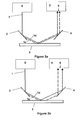
- a light source for a level sensor provides a beam 1 which includes p-polarised light and s-polarised light.
- Folding mirror 2 has a polarisation dependent Goos-Haenchen shift which causes p-polarised light to be translated (the s-polarised light is not translated).
- the beam is separated into two: a translated p-polarised beam as represented by broken line 1c, and an untranslated s-polarised beam as represented by the dotted line 1d.
- the surface of the substrate 3 reflects the p-polarised beam with an additional slight translation (the s-polarised beam is not translated).
- the detector 5 detects the p-polarised and s-polarised beams as a single beam with a centre point 6 (assuming that p-polarised and s-polarised beams are of equal intensity).
- the detected height includes an apparent surface depression which is caused in part by the mirror 2 and in part by the substrate 3.
- Figure 3b shows the effect of using the same level sensor to detect a substrate 3 having a different surface.
- the mirror 2 has the same wavelength dependent Goos-Haenchen shift, but the substrate provides a much larger shift, with the result that the centre point 6 of the detected beam is shifted to the left.
- each level sensor will suffer a different apparent surface depression error, due to differences between the mirrors of the level sensors.
- the substrate 3 comprises a 'wafer stack' (i.e. a wafer coated with several process layers) it acts as a polarisation filter, preferentially reflecting s-polarised light.
- the intensities of the p-polarised beam 1c and the s-polarised beam 1d are not equal at the detector 5, causing a shift of the detected centre point 6.
- the mirror 4 will give rise to a polarisation dependent Goos-Haenchen shift.
- the beam 1 is not a single wavelength but comprises a broad band of wavelengths.
- the broad band is used because it has been found in the past to reduce apparent surface depression (via averaging of the wavelength dependent Goos-Haenchen shift).
- a wavelength dependent Goos-Haenchen shift arises at each of the folding mirrors 2,4 and at the surface of the substrate 3.
- the folding mirrors 2,4 and especially the substrate 3 may act as wavelength filters.
- the polarisation dependent and wavelength dependent Goos-Haenchen shifts, together with the polarisation dependent and wavelength dependent filtering, provided by the folding mirrors 2, 4 and the substrate 3 give rise to an apparent surface depression which has an extremely complicated process dependency.
- the apparent surface depression has been found to vary from process to process (i.e. from processed substrate to processed substrate) and from level sensor to level sensor. It had not previously been realised until now that the mirrors provide a significant contribution to the process dependent apparent surface depression.
- the inventors have realised that this contribution may be mitigated by controlling those parameters of the mirrors which give rise to the Goos-Haenchen shift via the selection of appropriate mirrors.
- the selection of appropriate mirrors has a threefold benefit.
- the mirrors may be selected to provide a level sensor which has a reduced apparent surface depression (for a variety of processed substrates), thereby providing improved level sensing for a given level sensor.
- the mirrors may be selected to provide a level sensor which has apparent surface depression which is robust to small process variations (for example resist and oxide thickness variations). Particularly when levelling needs to be corrected for apparent surface depression by correction values, fewer measurements are needed to determine these correction values as these are applicable on other fields and wafers with the same product.
- level sensors are provided for a multiplicity of lithography apparatus, the mirrors of the levels sensors having substantially identical optical properties.
- the mirrors may be metallic, for example Ag, and may be provided with a coating, for example Al 2 O 3 (other coating materials may be used).
- the coating has been found by the inventors to give rise to a Goos-Haenchen shift, the wavelength and polarisation dependency of the shift being dependent upon the thickness of the coating. Therefore in this embodiment of the invention the thickness of the coating of the mirrors used for the level sensor is controlled to provide a minimised Goos-Haenchen shift (appropriate thicknesses of Al 2 O 3 are described further below).
- a 'family' of level sensors (and the lithographic apparatus to which they are fitted) may be defined for which the mirrors of the level sensors are substantially identical. For example, it may be specified that the mirrors are all fabricated together in a single batch.
- mirrors having an aluminium coating that is covered with a native oxide This native oxide grows naturally after deposition of the aluminium coating, when the aluminium coating is exposed to air.
- the thickness of the aluminium oxide will remain small, typically less than 10nm. It has been found that a thickness of this order provides a Goos-Haenchen shift.
- the thickness of the coating is very consistent from mirror to mirror, thereby providing mirrors with substantially identical properties. It is not desirable to provide a native oxide coating on Ag mirrors, since this will lead to blackening of the surface of the mirrors.
- level sensor mirrors having substantially identical optical properties may be obtained by using Au mirrors. No coating is needed on Au mirror surfaces, with the result that the Goos-Haenchen shift caused by the mirrors is substantially identical from mirror to mirror.
- a calibration of apparent surface depression may be performed for a lithography apparatus for a substrate to which a particular process (process A) has been applied.
- the calibration is used for that lithography apparatus each time a substrate is used to which process A has been applied.
- the calibration is time consuming and costly.
- a level sensor of a second lithography apparatus would need to be calibrated separately for process A, and similarly for third, fourth lithography apparatus, etc.
- the first aspect of the invention is applied, i.e. where the mirrors of the level sensors have substantially identical properties, only one level sensor must be calibrated for process A, and the resulting calibration is used for all of the level sensors (i.e.
- An embodiment of a second aspect of the invention comprises a level sensor provided with mirrors having optical properties which are selected to minimise process dependent apparent surface depression.
- the second aspect of the invention may be embodied in a level sensor having metallic mirrors.
- the level sensor comprises a source S, a detector 5, and folding mirrors 2, 4 comprising an Ag substrate with a Al 2 O 3 coating (other suitable coatings may be used). Coatings have been found by the inventors to give rise to a Goos-Haenchen shift, the wavelength and polarisation dependency of the shift being dependent upon the thickness of the coating. Therefore in this embodiment of the invention the thickness of the Al 2 O 3 coating of the mirrors used for the level sensor is selected to provide a minimised Goos-Haenchen shift.
- figure 4 shows an alternative level sensor to which the invention may be applied.
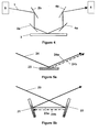
- a level sensor comprises a source S, detector 5 and four folding mirrors 2a, 2b, 4a, 4b. It can be seen that the level sensor shown in figure 4 corresponds to that shown in figure 2, except that each folding mirror 2, 4 is replaced with a pair of folding mirrors 2a, 2b, and 4a, 4b.
- the beam-steering optics may for example comprise a prism arranged to allow a beam to enter the prism, and then undergo internal reflection from a face of the prism before leaving the prism at a different angle.
- the prism may be provided with a coating on the external side of the face which provides the reflection, the coating being controlled according to the invention to provide a minimal Goos-Haenchen shift. Additionally or alternatively, the angle of incidence of the beam into the prism may be adjusted to reduce the Goos-Haenchen shift arising at the prism.
- the metallic mirrors are replaced with fully dielectric mirrors, i.e. mirrors comprising a non-conducting medium.
- Dielectric mirrors have a zero Goos-Haenchen effect, and so do not contribute to apparent surface depression.
- Apparent surface depression only occurs for reflecting surfaces that cause a phase jump of reflected light which is dependent on the angle of incidence.
- apparent surface depression only occurs when the following condition is satisfied: ⁇ ⁇ i ⁇ 0, where ⁇ is the phase jump (the argument of the complex reflection coefficient) and ⁇ i is the angle of incidence of the light beam. For a boundary between air and a dielectric medium (with a purely real refractive index) the derivative is zero.
- a disadvantage of using dielectric mirrors is that they preferentially reflect s-polarised light, with the result that apparent surface depression caused by the surface of the wafer is accentuated (the averaging effect provided by using all polarisations is lost).
- An advantage of using dielectric mirrors is that, since the apparent surface depression is caused entirely by the surface of the wafer, machine to machine variations of the apparent surface depression are substantially eliminated.
- the dielectric mirror used by the embodiment of the invention comprises a silicon slab which has an anti-reflective coating on its reverse side.
- the reflection loss caused by the silicon is at an acceptably low level.
- Dielectric mirrors may be implemented using any suitable material.
- the embodiment may for example be of the type shown in figure 2 or the type shown in figure 4.
- each folding mirror of the level sensor may be replaced with a pair of metallic mirrors.
- Each pair of metallic mirrors provides a zero net Goos-Haenchen shift, because the mirrors are arranged so that the second mirror provides a Goos-Haenchen shift which is opposite to that provided by the first mirror.
- An example of a suitable pair of mirrors is shown in figure 5b. Referring to figure 5b, a pair of identical metallic mirrors 21, 22 are symmetrically arranged so that a beam of light 23 is incident upon both mirrors with the same angle of incidence.
- the metallic mirrors 21, 22 are identical, including having the same thickness of coating layer, the Goos-Haenchen shift caused by each mirror cancels out to give a net apparent surface depression of zero. This is effective for every wavelength and every polarisation state, due to the symmetry of the mirror arrangement.
- the effect of the mirrors 21, 22 can be understood by comparing them with a single mirror, as shown in figure 5a.
- a beam 24 is incident upon a mirror 25.
- P-polarised light of the beam is translated by the mirror 25 upon reflection, whereas s-polarised light of the beam is not.
- This gives rise to an s-polarised beam 24a and a p-polarised beam 24b which are spatially separated.
- the Goos-Haenchen shift at mirror 22 gives rise to an s-polarised beam 23a and a p-polarised beam 23b.
- an equal and opposite Goos-Haenchen shift occurs at mirror 21, so that the beams 23a, 23b are recombined to form a single beam 23.
- a disadvantage of this embodiment of the invention, and of that shown in figure 5, is that it occupies extra space as compared to the embodiment of the invention shown in figure 2.
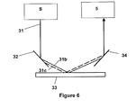
- a level sensor is constructed using two non-identical metallic mirrors which are chosen such that the Goos-Haenchen shift occurring at the first mirror is at least partially corrected by the Goos-Haenchen shift occurring at the second mirror, thereby leading to a minimal apparent surface depression.
- a first mirror 32 of the level sensor gives rise to a shift of the reflection of p-polarised light 31c but not s-polarised light 31b, whereas a second mirror 34 of the level sensor gives rise to a shift of the reflection of s-polarised light 31b but not p-polarised light 31c (for simplicity of illustration a substrate 33 is assumed not to give rise to any shift).
- the net apparent surface depression caused by the mirrors 32, 34 is zero.
- Variables which are independent of the mirrors are the angle of incidence of the level sensor beam on the mirrors, the wavelength range of the level sensor beam and the polarisation state of the level sensor beam. Variables of the mirrors themselves are the number of coating layers on the mirrors and the thickness of each coating layer.
- the inventors have modelled the effect of coating layer thickness for a level sensor comprising two folding mirrors based on a Ag substrate with an Al 2 O 3 coating, in a level sensor which uses an unpolarised light beam in the wavelength range 600-1050nm (generated by a halogen lamp).
- the angle of incidence of the light on the folding mirrors was 55 degrees.
- the level sensor performance was modelled in relation to a substrate comprising photoresist on silicon and photoresist on aluminium.
- the angle of incidence of the light on the substrate was 70 degrees.
- the apparent surface depression caused by the mirrors was determined for a range of resist thicknesses (200-1000nm), first for the silicon and photoresist substrate then for the aluminium and photoresist substrate. This gave two sets of apparent surface depression values. A set of difference values was obtained by subtracting the second set from the first set, and a weighted average of the set was obtained. The model did not include apparent surface depression caused by the substrate.
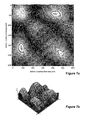
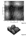
- the graphs shown in figure 7 illustrate that the apparent surface depression exhibits maxima and minima as a function of mirror coating thickness.
- a peak (light grey region in figure 7a) is indicative of a large error
- a trough (dark grey region in figure 7a) is indicative of a small error. It can been seen from figure 7 that all minima are found for non-identical coating thickness combinations.
- the data shown in figure 7 is complex it can be seen that in general terms a reasonably low error will be achieved provided that one of the mirrors is provided with a coating that is around 140nm thicker or thinner than the coating of the other mirror.
- a first mirror may have a coating which is 70nm thick and the second mirror may have a coating which is 210nm thick.
- This model indicates mirror-coating thicknesses which will give rise to a minimal apparent surface depression, assuming that no apparent surface depression is caused by the substrate. In practice it is known that the substrate will always give rise to some apparent surface depression, and so this model is of limited utility. The model is however useful to determine appropriate mirror-coating thicknesses for a level sensor to be fitted in a lithographic apparatus which will be used for a wide variety of processed substrates (since it may not be possible to model the apparent surface depression caused by the substrates).
- a lithographic apparatus will be used for a particular given processed substrate.
- a model may be used to determine the thickness of mirror coatings which provides a minimal apparent surface depression, taking into account the apparent surface depression caused by the substrate.
- the range of solutions for optimum coating stack parameters is large.
- the optimum choice depends on the angle of incidence of the level sensor beam on the mirrors, the wavelength range and polarisation state of the level sensor beam, the number of coating layers on the mirrors and the thickness of each coating layer. Additional variables are the angle of incidence of the level sensor beam on the substrate, and the expected combination of materials on the substrate.
- the inventors have constructed a second model, for a level sensor having two folding mirrors based on a Ag substrate with an Al 2 O 3 coating, a level sensor beam comprising unpolarised light in the wavelength range 600-1050nm, and a substrate comprising photoresist on silicon and photoresist on aluminium.
- the angle of incidence of the light on the folding mirrors was 55 degrees.
- the angle of incidence of the light on the substrate was 70 degrees.
- the coating thickness is centred on 275nm with a tolerance of +/- 40nm.
- Modern coating methods may allow the thickness to be controlled with a tolerance of +/- 20nm. This is preferred because it allows the coating thicknesses to be kept close to the preferred value of 275nm.
- the choice of the preferred value of 275nm is erroneous, since it does not correspond precisely with the minimum error.
- the choice of 275nm is optimal based on a combination of a small error and a small gradient.
- a low error occurs in regions where one mirror has a coating thickness of approximately 275nm and the other has a coating thickness of approximately 520nm. This region may also be used to achieve a low error, although it may be difficult to control the thickness of the coating at 520nm (the thicker a coating is, the harder it is to control the thickness).
- the second model was determined for a particular substrate, i.e. photoresist-on-silicon with a thickness range of 200nm-600nm.
- the model may be used to select appropriate mirrors for the level sensor, for example with coatings 275nm thick.
- the model may be modified to determine appropriate mirrors for the level sensor. In this way the mirrors may be tailored to be optimal for those processed substrates for which it is intended to use a given lithographic apparatus.
- FIG. 9 shows the results generated by the model. Referring to figure 9 it can be seen that areas with minimal machine-to-machine error are centred on oxide thicknesses of 75nm and 240nm for both mirrors, or a combination of 75nm on one mirror and 240nm on the other mirror.
- the results shown in figure 9 are in effect Al 2 O 3 thicknesses which are optimised for manufacturing tolerances.
- the best thickness for the coating is 275nm.
- the accuracy with which the coating thicknesses can be applied may vary from +/-40nm to +/- 20nm.
- a first mirror may have a coating which is 90nm thick and the second mirror may have a coating which is 220nm thick. These values differ slightly from those obtained in relation to figure 7. This is in order to provide an improved machine-to-machine variation.
- the accuracy with which these coating thicknesses can be applied may vary from +/-40nm to +/- 20nm.
- Machine-to-machine variation is improved by increasing the accuracy with which the thickness of the coating is controlled. This is another reason why well controlled thicknesses are preferred.
- the preferred values of coating thickness may be dependent upon the angle of incidence of light on the folding mirrors of the level sensor, or on the angle of incidence of the light on the substrate. Both of these have been investigated using the model developed by the inventors. It was found that variation by +/- 5 degrees of the angle of incidence of light on the folding mirrors (55 degrees) did not significantly modify the output of the model. Similarly, it was found that variation by +/- 5 degrees of the angle of incidence of the light on the substrate (70 degrees) did not significantly modify the output of the model. It can be concluded therefore that the selection of the coatings for the mirrors is applicable for a substantial range of angles of incidence.
- the preferred values of coating thickness were determined using a model based upon Ag mirrors. The inventors have substituted Al mirrors for the Ag mirrors, and have found that the preferred values of coating thickness remain the same.
- the preferred values of coating thickness were determined using Al 2 O 3 . It will be appreciated that different materials may be used to provide the coating, for example SiO 2 or MgF 2 . An important property of the material is that it is transparent, i.e. sufficiently transparent at the wavelength or wavelengths generated by the light source to enable the level sensor to function correctly. Where a material other than Al 2 O 3 is used, the preferred values of the coating thickness should be adjusted to take account of differences of refractive index between the material used and Al 2 O 3 . In other words, the optical thickness of the oxide layer should be equivalent to that of the Al 2 O 3 layer.
- the term 'optical thickness' is intended to mean the product of the thickness of a material and the refractive index of that material.
- the refractive index of Al 2 O 3 is 1.57 at a wavelength of 800nm (this is the central wavelength of the light used by the level sensor of the embodiment of the invention).
- the optical thickness of a 275nm layer of Al 2 O 3 is therefore 275 x 1.57, which is 432nm.
- the thickness of the material should be selected to provide an optical thickness of 432nm.
Landscapes
- Physics & Mathematics (AREA)
- General Physics & Mathematics (AREA)
- Exposure And Positioning Against Photoresist Photosensitive Materials (AREA)
- Exposure Of Semiconductors, Excluding Electron Or Ion Beam Exposure (AREA)
Priority Applications (1)
| Application Number | Priority Date | Filing Date | Title |
|---|---|---|---|
| EP04075080A EP1439428A3 (fr) | 2003-01-14 | 2004-01-13 | Détecteur de niveau pour un appareil lithographique |
Applications Claiming Priority (3)
| Application Number | Priority Date | Filing Date | Title |
|---|---|---|---|
| EP03075118 | 2003-01-14 | ||
| EP03075118 | 2003-01-14 | ||
| EP04075080A EP1439428A3 (fr) | 2003-01-14 | 2004-01-13 | Détecteur de niveau pour un appareil lithographique |
Publications (2)
| Publication Number | Publication Date |
|---|---|
| EP1439428A2 true EP1439428A2 (fr) | 2004-07-21 |
| EP1439428A3 EP1439428A3 (fr) | 2009-05-13 |
Family
ID=32598812
Family Applications (1)
| Application Number | Title | Priority Date | Filing Date |
|---|---|---|---|
| EP04075080A Withdrawn EP1439428A3 (fr) | 2003-01-14 | 2004-01-13 | Détecteur de niveau pour un appareil lithographique |
Country Status (1)
| Country | Link |
|---|---|
| EP (1) | EP1439428A3 (fr) |
Cited By (2)
| Publication number | Priority date | Publication date | Assignee | Title |
|---|---|---|---|---|
| US8432554B2 (en) | 2005-11-15 | 2013-04-30 | Nikon Corporation | Surface position detecting apparatus, exposure apparatus and device manufacturing method |
| WO2020182488A1 (fr) * | 2019-03-13 | 2020-09-17 | Asml Holding N.V. | Appareil lithographique, appareil de métrologie, système optique et procédé |
Family Cites Families (14)
| Publication number | Priority date | Publication date | Assignee | Title |
|---|---|---|---|---|
| DE1179640B (de) * | 1961-10-16 | 1964-10-15 | Ibm Deutschland | Anordnung zur Lichtsteuerung |
| JPS58113706A (ja) * | 1981-12-26 | 1983-07-06 | Nippon Kogaku Kk <Nikon> | 水平位置検出装置 |
| JP2785146B2 (ja) * | 1990-02-09 | 1998-08-13 | キヤノン株式会社 | 自動焦点調整制御装置 |
| JP2748066B2 (ja) * | 1992-04-23 | 1998-05-06 | 富士写真光機株式会社 | 反射鏡 |
| JPH06260393A (ja) * | 1993-03-09 | 1994-09-16 | Hitachi Ltd | 位置決め装置 |
| JPH07168008A (ja) * | 1993-12-13 | 1995-07-04 | Nikon Corp | Ag表面鏡 |
| SG102627A1 (en) * | 1996-11-28 | 2004-03-26 | Nikon Corp | Lithographic device |
| JPH10209039A (ja) * | 1997-01-27 | 1998-08-07 | Nikon Corp | 投影露光方法及び投影露光装置 |
| DE19838826B4 (de) * | 1998-08-26 | 2005-03-03 | Fraunhofer-Gesellschaft zur Förderung der angewandten Forschung e.V. | Optisches Element mit transparenter, kratzfester Beschichtung, Verfahren und Vorrichtung zu seiner Herstellung sowie dessen Verwendung |
| JP2001343510A (ja) * | 2000-06-02 | 2001-12-14 | Canon Inc | 金属反射鏡およびその製造方法 |
| US6470109B1 (en) * | 2000-06-08 | 2002-10-22 | Agilent Technologies, Inc. | Determining waveguide positions and angles for efficient reflective coupling |
| JP3890233B2 (ja) * | 2002-01-07 | 2007-03-07 | キヤノン株式会社 | 位置決めステージ装置、露光装置及び半導体デバイスの製造方法 |
| EP1357435A1 (fr) * | 2002-04-23 | 2003-10-29 | ASML Netherlands B.V. | Appareil lithographique et méthode de fabrication d'un dispositif |
| KR101157002B1 (ko) * | 2002-12-10 | 2012-06-21 | 가부시키가이샤 니콘 | 노광 장치 및 디바이스 제조 방법 |
-
2004
- 2004-01-13 EP EP04075080A patent/EP1439428A3/fr not_active Withdrawn
Cited By (4)
| Publication number | Priority date | Publication date | Assignee | Title |
|---|---|---|---|---|
| US8432554B2 (en) | 2005-11-15 | 2013-04-30 | Nikon Corporation | Surface position detecting apparatus, exposure apparatus and device manufacturing method |
| US9594316B2 (en) | 2005-11-15 | 2017-03-14 | Nikon Corporation | Surface positioning detecting apparatus, exposure apparatus and device manufacturing method |
| WO2020182488A1 (fr) * | 2019-03-13 | 2020-09-17 | Asml Holding N.V. | Appareil lithographique, appareil de métrologie, système optique et procédé |
| US11537055B2 (en) | 2019-03-13 | 2022-12-27 | Asml Holding N.V. | Lithographic apparatus, metrology apparatus, optical system and method |
Also Published As
| Publication number | Publication date |
|---|---|
| EP1439428A3 (fr) | 2009-05-13 |
Similar Documents
| Publication | Publication Date | Title |
|---|---|---|
| US7248337B2 (en) | Lithographic apparatus, level sensor, method of inspection, device manufacturing method, and device manufactured thereby | |
| US7466413B2 (en) | Marker structure, mask pattern, alignment method and lithographic method and apparatus | |
| US6795163B2 (en) | Lithographic manufacturing process, lithographic projection apparatus, and device manufactured thereby | |
| JP2004289123A (ja) | リソグラフ装置およびデバイス製造方法 | |
| EP1477851A1 (fr) | Méthode de fabrication d'un dispositif et appareil lithographique | |
| US6906785B2 (en) | Lithographic apparatus, device manufacturing method, and device manufactured thereby | |
| JP3978191B2 (ja) | 傾斜感度が低減されたウェハアライメント装置および方法 | |
| US7391502B2 (en) | Lithographic apparatus, device manufacturing method, and method of manufacturing a component | |
| US7084952B2 (en) | Lithographic apparatus, device manufacturing method, and computer-readable storage medium | |
| EP1491961B1 (fr) | Appareil lithographique et méthode de fabrication d'un dispositif | |
| US8252487B2 (en) | Device manufacturing method and mask for use therein | |
| EP1439428A2 (fr) | Détecteur de niveau pour un appareil lithographique | |
| US6954257B2 (en) | Lithographic apparatus and device manufacturing method | |
| EP1426826A2 (fr) | Appareil lithographique et procédé pour la production d'un dispositif | |
| EP1164436A2 (fr) | Opération d'un appareil de projection lithographique | |
| EP1400860B1 (fr) | Structure d'une marque lithograhique, appareil de projection lithographique comprenant une telle structure et procédé d'alignement d'un substrat utilisant une telle structure | |
| US6788383B1 (en) | Lithographic apparatus, device manufacturing methods, and computer-readable storage medium | |
| WO2008147175A1 (fr) | Appareil lithographique et procédé de fabrication de dispositif | |
| EP1357435A1 (fr) | Appareil lithographique et méthode de fabrication d'un dispositif | |
| EP1394815B1 (fr) | Appareil de lithographie comprenant une multicouche Mo/Si couvert par une couche protectrice | |
| EP1426823A1 (fr) | Appareil lithographique, procédé pour la production d'un dispositf et dispositif produit par ce procédé | |
| EP1318431A1 (fr) | Appareil lithographique, méthode de fabrication d'un dispositif, et méthode de fabrication d'un élément optique | |
| EP1450211A2 (fr) | Dispositif et méthode d'alignement d'une tranche de semiconducteur ayant une sensibilité à l'inclinaison réduite | |
| EP1398670A2 (fr) | Procédé d'alignement d'un substrat, programme informatique et procédé pour la production d'un dispositif | |
| EP1498779A2 (fr) | Structure d'une marque d'alignement ou de recouvrement |
Legal Events
| Date | Code | Title | Description |
|---|---|---|---|
| PUAI | Public reference made under article 153(3) epc to a published international application that has entered the european phase |
Free format text: ORIGINAL CODE: 0009012 |
|
| AK | Designated contracting states |
Kind code of ref document: A2 Designated state(s): AT BE BG CH CY CZ DE DK EE ES FI FR GB GR HU IE IT LI LU MC NL PT RO SE SI SK TR |
|
| AX | Request for extension of the european patent |
Extension state: AL LT LV MK |
|
| RIN1 | Information on inventor provided before grant (corrected) |
Inventor name: QUEENS, RENE MARINUS GERARDUS JOHAN Inventor name: BROODBAKKER, PETRUS JOHANNES MARIA Inventor name: TEUNISSEN, PAULUS ANTONIUS ANDREAS |
|
| RAP1 | Party data changed (applicant data changed or rights of an application transferred) |
Owner name: ASML NETHERLANDS B.V. |
|
| PUAL | Search report despatched |
Free format text: ORIGINAL CODE: 0009013 |
|
| AK | Designated contracting states |
Kind code of ref document: A3 Designated state(s): AT BE BG CH CY CZ DE DK EE ES FI FR GB GR HU IE IT LI LU MC NL PT RO SE SI SK TR |
|
| AX | Request for extension of the european patent |
Extension state: AL LT LV MK |
|
| RIC1 | Information provided on ipc code assigned before grant |
Ipc: G03F 9/00 20060101ALI20090406BHEP Ipc: G03F 7/20 20060101AFI20040426BHEP |
|
| STAA | Information on the status of an ep patent application or granted ep patent |
Free format text: STATUS: THE APPLICATION IS DEEMED TO BE WITHDRAWN |
|
| AKX | Designation fees paid |
Designated state(s): DE FR GB IT NL |
|
| 18D | Application deemed to be withdrawn |
Effective date: 20090801 |