EP1499172B1 - Elektromagnetisch abgeschirmte schaltungseinrichtung und abschirmverfahren dafür - Google Patents
Elektromagnetisch abgeschirmte schaltungseinrichtung und abschirmverfahren dafür Download PDFInfo
- Publication number
- EP1499172B1 EP1499172B1 EP03720949A EP03720949A EP1499172B1 EP 1499172 B1 EP1499172 B1 EP 1499172B1 EP 03720949 A EP03720949 A EP 03720949A EP 03720949 A EP03720949 A EP 03720949A EP 1499172 B1 EP1499172 B1 EP 1499172B1
- Authority
- EP
- European Patent Office
- Prior art keywords
- circuit board
- ground connection
- shield pack
- electrically conductive
- shield
- Prior art date
- Legal status (The legal status is an assumption and is not a legal conclusion. Google has not performed a legal analysis and makes no representation as to the accuracy of the status listed.)
- Expired - Lifetime
Links
- 238000000034 method Methods 0.000 title claims description 30
- 239000000463 material Substances 0.000 claims description 13
- 239000004020 conductor Substances 0.000 claims description 10
- 239000000853 adhesive Substances 0.000 claims description 8
- 238000010438 heat treatment Methods 0.000 claims description 5
- 230000005611 electricity Effects 0.000 claims 1
- 229910052751 metal Inorganic materials 0.000 description 28
- 239000002184 metal Substances 0.000 description 28
- 239000011347 resin Substances 0.000 description 19
- 229920005989 resin Polymers 0.000 description 19
- 239000010408 film Substances 0.000 description 16
- 239000004065 semiconductor Substances 0.000 description 11
- 238000010586 diagram Methods 0.000 description 7
- 230000000694 effects Effects 0.000 description 4
- 230000001070 adhesive effect Effects 0.000 description 3
- 229910052782 aluminium Inorganic materials 0.000 description 3
- XAGFODPZIPBFFR-UHFFFAOYSA-N aluminium Chemical compound [Al] XAGFODPZIPBFFR-UHFFFAOYSA-N 0.000 description 3
- 238000004519 manufacturing process Methods 0.000 description 3
- 238000007789 sealing Methods 0.000 description 3
- 229920001187 thermosetting polymer Polymers 0.000 description 3
- 239000010409 thin film Substances 0.000 description 3
- 230000006870 function Effects 0.000 description 2
- 125000000524 functional group Chemical group 0.000 description 2
- 239000003973 paint Substances 0.000 description 2
- 238000007747 plating Methods 0.000 description 2
- 239000000126 substance Substances 0.000 description 2
- OKTJSMMVPCPJKN-UHFFFAOYSA-N Carbon Chemical compound [C] OKTJSMMVPCPJKN-UHFFFAOYSA-N 0.000 description 1
- 238000005520 cutting process Methods 0.000 description 1
- 230000007547 defect Effects 0.000 description 1
- 238000000151 deposition Methods 0.000 description 1
- 238000005516 engineering process Methods 0.000 description 1
- 229910002804 graphite Inorganic materials 0.000 description 1
- 239000010439 graphite Substances 0.000 description 1
- 238000009413 insulation Methods 0.000 description 1
- 230000010354 integration Effects 0.000 description 1
- WABPQHHGFIMREM-UHFFFAOYSA-N lead(0) Chemical compound [Pb] WABPQHHGFIMREM-UHFFFAOYSA-N 0.000 description 1
- 230000004048 modification Effects 0.000 description 1
- 238000012986 modification Methods 0.000 description 1
- 230000000149 penetrating effect Effects 0.000 description 1
- 229920000642 polymer Polymers 0.000 description 1
- 230000005855 radiation Effects 0.000 description 1
- 230000035939 shock Effects 0.000 description 1
- 229910052709 silver Inorganic materials 0.000 description 1
- 239000004332 silver Substances 0.000 description 1
- 229910000679 solder Inorganic materials 0.000 description 1
- 230000003313 weakening effect Effects 0.000 description 1
Images


Classifications
-
- H—ELECTRICITY
- H05—ELECTRIC TECHNIQUES NOT OTHERWISE PROVIDED FOR
- H05K—PRINTED CIRCUITS; CASINGS OR CONSTRUCTIONAL DETAILS OF ELECTRIC APPARATUS; MANUFACTURE OF ASSEMBLAGES OF ELECTRICAL COMPONENTS
- H05K3/00—Apparatus or processes for manufacturing printed circuits
- H05K3/22—Secondary treatment of printed circuits
- H05K3/28—Applying non-metallic protective coatings
- H05K3/284—Applying non-metallic protective coatings for encapsulating mounted components
-
- H—ELECTRICITY
- H05—ELECTRIC TECHNIQUES NOT OTHERWISE PROVIDED FOR
- H05K—PRINTED CIRCUITS; CASINGS OR CONSTRUCTIONAL DETAILS OF ELECTRIC APPARATUS; MANUFACTURE OF ASSEMBLAGES OF ELECTRICAL COMPONENTS
- H05K9/00—Screening of apparatus or components against electric or magnetic fields
- H05K9/0007—Casings
- H05K9/002—Casings with localised screening
- H05K9/0039—Galvanic coupling of ground layer on printed circuit board [PCB] to conductive casing
-
- H—ELECTRICITY
- H05—ELECTRIC TECHNIQUES NOT OTHERWISE PROVIDED FOR
- H05K—PRINTED CIRCUITS; CASINGS OR CONSTRUCTIONAL DETAILS OF ELECTRIC APPARATUS; MANUFACTURE OF ASSEMBLAGES OF ELECTRICAL COMPONENTS
- H05K1/00—Printed circuits
- H05K1/02—Details
- H05K1/0213—Electrical arrangements not otherwise provided for
- H05K1/0216—Reduction of cross-talk, noise or electromagnetic interference
- H05K1/0218—Reduction of cross-talk, noise or electromagnetic interference by printed shielding conductors, ground planes or power plane
-
- H—ELECTRICITY
- H05—ELECTRIC TECHNIQUES NOT OTHERWISE PROVIDED FOR
- H05K—PRINTED CIRCUITS; CASINGS OR CONSTRUCTIONAL DETAILS OF ELECTRIC APPARATUS; MANUFACTURE OF ASSEMBLAGES OF ELECTRICAL COMPONENTS
- H05K2201/00—Indexing scheme relating to printed circuits covered by H05K1/00
- H05K2201/01—Dielectrics
- H05K2201/0104—Properties and characteristics in general
- H05K2201/0125—Shrinkable, e.g. heat-shrinkable polymer
-
- H—ELECTRICITY
- H05—ELECTRIC TECHNIQUES NOT OTHERWISE PROVIDED FOR
- H05K—PRINTED CIRCUITS; CASINGS OR CONSTRUCTIONAL DETAILS OF ELECTRIC APPARATUS; MANUFACTURE OF ASSEMBLAGES OF ELECTRICAL COMPONENTS
- H05K2201/00—Indexing scheme relating to printed circuits covered by H05K1/00
- H05K2201/10—Details of components or other objects attached to or integrated in a printed circuit board
- H05K2201/10227—Other objects, e.g. metallic pieces
- H05K2201/10295—Metallic connector elements partly mounted in a hole of the PCB
- H05K2201/10303—Pin-in-hole mounted pins
-
- H—ELECTRICITY
- H05—ELECTRIC TECHNIQUES NOT OTHERWISE PROVIDED FOR
- H05K—PRINTED CIRCUITS; CASINGS OR CONSTRUCTIONAL DETAILS OF ELECTRIC APPARATUS; MANUFACTURE OF ASSEMBLAGES OF ELECTRICAL COMPONENTS
- H05K2203/00—Indexing scheme relating to apparatus or processes for manufacturing printed circuits covered by H05K3/00
- H05K2203/11—Treatments characterised by their effect, e.g. heating, cooling, roughening
- H05K2203/1189—Pressing leads, bumps or a die through an insulating layer
-
- H—ELECTRICITY
- H05—ELECTRIC TECHNIQUES NOT OTHERWISE PROVIDED FOR
- H05K—PRINTED CIRCUITS; CASINGS OR CONSTRUCTIONAL DETAILS OF ELECTRIC APPARATUS; MANUFACTURE OF ASSEMBLAGES OF ELECTRICAL COMPONENTS
- H05K2203/00—Indexing scheme relating to apparatus or processes for manufacturing printed circuits covered by H05K3/00
- H05K2203/13—Moulding and encapsulation; Deposition techniques; Protective layers
- H05K2203/1305—Moulding and encapsulation
- H05K2203/1311—Foil encapsulation, e.g. of mounted components
Definitions
- the present invention relates to a circuit device which has been electromagnetically shielded, and a shielding method for shielding the circuit device.
- Electronic components such as semiconductor components, and functional groups such as to analog circuits and wireless circuits have been mounted on a printed circuit board.
- a printed circuit board is electromagnetically shielded
- either the electronic component or the functional group to be electromagnetically shielded is covered by a case made of metal, and the metal case is electrically connected to a ground terminal of the printed circuit board by way of solder.
- the metal case there is a case that a cover made of resin and having an inner plated metal layer may be employed.
- an electromagnetic wave absorbing sheet capable of weakening electromagnetic waves may be employed.
- the electromagnetic shielding effect is small.
- this method cannot solve electromagnetic interference among the respective electronic components, but also cannot reinforce the printed circuit board.
- an electromagnetic shielding method is disclosed in Japanese Laid Open Utility Model Application ( JU-A-Heisei 2-45699 ).
- insulating films are formed on surfaces of a circuit board on which electronic components are mounted.
- an electrically conductive shield films are formed on the insulating films.
- the electrically conductive shield films are connected to an earth line formed on the electronic circuit board.
- JP-A-Heisei 4-58596 another electromagnetic shielding method is disclosed in Japanese Laid Open patent Application ( JP-A-Heisei 4-58596 ).
- electronic circuit components on the printed circuit board is partitioned by electric conductors which are connected to a ground portion of the printed circuit board to prevent mutual electromagnetic inference between the electronic circuit components.
- the printed circuit board and the entire of electronic circuit components mounted on this printed-wiring board are covered by an insulating sealing resin or an insulating thin-film seal, which can be easily peeled later.
- a portion of the electric conductor is exposed from the sealing resin or the thin-film seal.
- a metal plating layer or an electrically conductive paint layer is coated on the sealing resin or the thin-film seal in such a manner that the metal plating layer or the electrically conductive paint layer is connectable to the electric conductor.
- JP-A-Heisei 4-72698 a shielding device is disclosed in Japanese Laid Open Patent Application (JP-A-Heisei 4-72698).
- JP-A-Heisei 4-72698 a shielding device is disclosed in Japanese Laid Open Patent Application.
- a portion of a printed circuit board where electronic components are mounted is covered by a bag made of thermal shrinkage resin.
- An electrically conductive film has been formed on the outer surface of this bag.
- a ground pattern formed on an exposed portion of the printed circuit board is connected to the electrically conductive film by a lead wire.
- JP-P2000-223647A a method of manufacturing a high frequency module is disclosed in Japanese Laid Open Patent Application ( JP-P2000-223647A ).
- a printed circuit board is provided on which electronic components have been mounted and a ground terminal having a predetermined height has been formed.
- One surface side of the printed circuit board on which electronic components have been mounted is covered by a stacked sheet in which an insulating resin film and an electrically conductive film having the shield effect are laminated.
- the printed circuit board is heated so as to soften the insulating resin film, so that the ground terminal and the electrically conductive film are electrically connected.
- JP-A-9 051 192 it is disclosed to cover a circuit board with an electrically conductive heat shrink tube and, subsequently, to apply heat in order to shrink the tube.
- a memory module is disclosed in Japanese Laid Open Patent Application ( JP-P2000-251463A ).
- a memory chip is mounted on a portion of one surface of a printed circuit board. This portion of one surface of the printed circuit board is covered by a shield sheet formed by stacking an adhesive sheet and an aluminum sheet.
- the shield sheet is adhered on the upper surface of the memory chip and the upper surface of the printed circuit board so that the semiconductor memory chip is electromagnetically shielded and is fixed on the printed circuit board.
- electromagnetic noise radiated from the memory chip is shielded by the aluminum sheet.
- the aluminum sheet functions as a heat radiating plate, so that the heat radiation of the memory module may be improved.
- a shielding film is applied onto a circuit board.
- the shielding film comprises an insulating layer and an electrically conductive layer.
- An electric contact between the electrically conductive layer and the circuit board is established by using a conductive substance such as a graphite paste or a polymer containing silver. This substance is brought in contact with the electrically conductive layer by using a sharp spike penetrating the shielding film.
- a further shielding enclosure for a circuit board is described in EP-A-0 802 710 .
- the material sheet of this shielding enclosure comprises an insulating layer and a metallic layer which is electrically connected to a grounding pad on the circuit board.
- the shielding enclosure has an opening. Trough this opening, the electric contact between the metallic layer and the grounding pad is established by using a conductive adhesive which is applied prior to connecting the edges of the material sheet, and, thus, prior to forming the enclosure itself
- a circuit board which is enveloped in a folded sheet material.
- the sheet material comprises an insulating layer and an electrically conductive layer, the latter being earthed by a screw fastening the sheet material to a mounting frame.
- an object of the present invention is to provide an elelctromagnetically shielded circuit device in which electromagnetic shield can be accomplished simply and surely without preventing high density integration of electronic components and a printed circuit board can be reinforced, and a shielding method of the circuit device.
- a method of shielding a circuit device includes the steps of claim 1.
- the base portion of the ground connection terminal may have a height which is substantially equal to a thickness of the shield pack. It is desirable that the bottom plane of the cone is connected to the electrically conductive layer when the tip portion breaks through the shield pack.
- the ground connection portion and the electrically conductive layer may be connected by passing an electrically conductive connection component through the ground connection portion between the shield pack and the circuit board, after the insulating layer of the shield pack is fitted with the electronic component and the circuit board.
- the circuit board may have a through-hole formed in the ground connection portion, and the through-hole is filled with an electric conductor connected to the ground connection portion. It is desirable that the connection component passes through the through-hole to connect the ground connection portion with the electrically conductive layer. It is desirable that the connection component is used to fix the circuit board contained within the shield pack to a housing, when the housing has an electrically conductive portion connected to the electrically conductive layer.
- the reducing step may include vacuum-sucking air contained in the shield pack such that the insulating layer of the shield pack contacts the electronic component and the circuit board.
- the reducing step may include vacuum-sucking air contained in the shield pack such that the insulating layer of the shield pack contacts the electronic component and the circuit board.
- an adhesive agent may be coated on at least a portion of the circuit board and at least a portion of an outer surface of the electronic component.
- the reducing step may include heating the shield pack such that the insulating layer of the shield pack contacts the electronic component and the circuit board.
- an electromagnetically shielded circuit device includes the features of claim 10 It is desirable that the base portion of the ground connection terminal has a height which substantially equals the thickness of the shield pack, and the bottom plane of the cone is connected to the electrically conductive layer under in a state that the tip portion breaks through the shield pack.
- the circuit board has a through-hole formed in the ground connection portion, the through-hole is filled with an electric conductor connected to the ground connection portion, and the connection component passes through the through-hole to connect the ground connection portion with the electrically conductive layer.
- connection component is a vis/screw used to fix the circuit board contained within the shield pack to a housing, and the housing has an electrically conductive portion connected to the electrically conductive layer.
- Fig. 1 is a sectional view showing the structure of a circuit device according to the first embodiment of the present invention.
- Fig. 2 is an enlarged view showing a ground connection terminal portion shown in Fig. 1 .
- Fig. 3 is a perspective view showing the structure of a printed circuit board on which electronic components shown in Fig. 1 have been mounted.
- Fig. 4 is an enlarged view showing a ground connection terminal shown in Fig. 3 .
- the circuit device is composed of a printed circuit board or a circuit board 1 as a major wiring board of a portable appliance which is strongly required to be made compact and slim.
- Mount components 2 such as an SMT (Surface Mount Technology) type electronic component
- semiconductor device components 3 such as an IC have been mounted on the printed circuit board 1 by way of a surface mounting system.
- ground connection terminals 5 are arranged on the printed circuit board 1 and provided on a ground connection pattern portion 21.
- the entire of the printed circuit board 1 on which electronic components such as the mount components 2 and the semiconductor device components 3 had been mounted is stored in a shield pack 4 and shielded.
- the ground connection terminals 5 penetrate through the shield pack 4.
- the shield pack 4 has a multi-layer structure formed of an insulating layer 9 as the innermost layer and a metal layer 8 as the outermost layer.
- the insulating layer 9 is formed on the inner side and the metal layer 8 is formed on the outer side, as shown in Fig. 2 .
- the insulating film 9 is formed of a thermosetting resin material such as a thermosetting resin film.
- the insulating layer 9 is hardened such that this insulating layer 9 is in close contact with the surfaces of the mount components 2, semiconductor device components 3, and printed circuit board 1.
- the metal film 8 is formed by vapor-depositing a metal on the insulating layer 9.
- the metal layer 8 has been previously formed on the insulating layer 9. Instead, the metal layer 8 may be formed after the ground connection terminals 5 have broken through the shield pack 4. The metal layer 8 is in contact to the ground connection terminals 5 penetrate through the shield pack 4, and are connected with the ground portion of the printed circuit board 1. At this time, in order to more firmly connect the metal layer 8 to the ground portion, the ground connection terminal 5 and the metal layer 8 may be soldered after the ground connection terminals 5 penetrate through the shield pack 4.
- the ground connection terminal 5 has a tip portion having a conical shape, and a base portion, and is previously planted in the printed circuit board on which the electronic components have been mounted.
- the base portion may be inserted to a half way of the printed circuit board 1 (not shown), or may be passed through the printed circuit board, as shown in Fig. 2 .
- the tip portion of the ground connection terminal 5 breaks through the shield pack 4, and is connected to the metal layer 8.
- the base portion of the ground connection terminal 5 has a step portion 10 having a height substantially equal to a thickness of the shield pack 4.
- the step portion 10 is formed in such a manner that the shield pack 4 cannot be easily extracted when the ground connection terminal 5 breaks through the shield pack 4.
- the ground connection terminal 5 is made of electrically conductive material characteristic such as metal, and is connected to the ground connection portion 21 of the printed circuit board 1.
- the ground connection terminal 5 functions as an electrode for electrically connecting the metal layer 8 of the shield pack 4 to the ground portion of the printed circuit board 1. It should be noted that the sectional area of the step portion 21 of the ground connection terminal 5 is smaller than the area of a bottom plane of the tip portion so as not to project from the base plane.
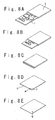
- Figs. 5A to 5D are step diagrams showing the shielding method of the circuit device according to the present invention.
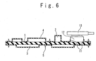
- Fig. 6 is a sectional view showing an example in which the external connection terminals are mounted on the circuit device according to this embodiment of the present invention.
- the entire of the printed circuit board 1 on which the electronic components have been mounted is inserted into the shield back 4 having a sack shape.
- a joint portion 6 of an opening portion of the shield pack 4 is adhered mainly to each other, and vacuum suction is carried out from a remaining opening portion 7 thereof.
- the inner capacity of the shield pack 4 is reduced, and the shield pack 4 is made in close contact to the surface of the printed circuit board 1 and the surfaces of the mount components.
- the shield pack 4 having sack shape has the insulating layer 9 on the inner side thereof, namely, on the side the shield pack 4 contacts the printed circuit board 1, and also has the metal layer 8 on the outer side thereof, namely, on the side where the shield pack 4 does not contact the printed circuit board 1. Since the vacuum suction is carried out, the insulating layer 9 is made to contact the mount components 2 and the semiconductor components 3, which have been mounted on the printed circuit board 1, along these mount components 2 and semiconductor components 3. It should be understood that there is no problem that the electrodes are electrically short-circuited, since the insulating layer 9 which contacts the mount component 2 and the semiconductor component 3 may play a role of electric insulation, even when the shield pack 4 is in contact with electrodes, the mount components 2 and the semiconductor device components 3.
- the shield pack 4 opposes the ground connection terminal 5, which is planted on the printed circuit board 1, and is flawed by the tip portion of the ground connection terminal 5 to form a hole in the vacuum suction.
- the ground connection terminal 5 penetrates through the shield pack 4, and contacts the metal layer 8 of the shield pack 4.
- the electromagnetic shield is achieved by the insulating layer 9 and the metal layer 8 of the shield pack 4.
- the shield pack 4 is fitted with the printed circuit board 1 on which the electronic components have been mounted, a heating operation is carried out, so that the shield pack 4 is hardened. It should be understood that since the shield pack 4 is put between the mount components 2 and the semiconductor components 3, the shield pack 4 is thermally hardened in such a manner that the strength of the entire printed circuit board 1 is reinforced, and occurrence of a defect can be prevented at a component joint portion when a shock is applied to the shield pack 4.
- a specific portion 11 of the shield pack 4 which is required to be externally connected to a connector may be cut away. As a result, a connector component 12 is exposed, so that an external connection terminal 13 can be mounted. A mechanical treatment such as cutting may be carried out every printed circuit board 1 within the shield pack 4.
- the effective electromagnetic shield can be formed only by fitting the shield pack 4 of the insulating layer 9 and the metal layer 8 to the printed circuit board 1 on which the electronic components have been mounted.
- the electromagnetic shield can be accomplished within the minimum space in the simple and firm manner without hindering the high density mounting of the electronic components.
- the printed circuit board 1 can be reinforced at the same time as the shield pack 4 is hardened in the state that it is in close contact to the printed circuit board 1.
- the shield pack 4 can be simply peeled even when any problem occurs in the printed circuit board 1 after the electromagnetic shield has been accomplished, and even when a part or entire of the printed circuit board 1 should be exposed in order to check and repair the electronic components. Also, this feature may avoid mischief since the shield pack 4 which has been once dismounted cannot be again mounted.
- Fig. 7A to Fig. 7C are manufacturing step diagrams showing a shielding method when a thermal shrinkage resin material is used for a shield pack in a circuit device according to the second embodiment mode of the present invention.
- the thermal shrinkage material is employed as the resin material of the insulating layer 9 of the shield pack 4.
- the thermal shrinkage resin material is used for the shield pack 4
- the entire portion of the printed circuit board 1 on which the electronic components have been mounted is inserted into the shield pack 4 having the sack shape.
- the shield pack 4 is heated by a heating air supplier 14, a reflow furnace, or the like, so that this shield pack 4 is thermally shrunk.
- the shield pack 4 closely contacts the printed circuit board 1.
- the ground connection terminal 5 is planted on the printed circuit board 1. However, a hole may be formed in the printed circuit board 1, and the printed circuit board 1 may be shielded by the shield pack 4, and thereafter, a pin or a screw may be inserted into the hole of the printed circuit board 1. In the third embodiment of the present invention, the ground connection terminal 5 is not provided on the printed circuit board 1. An electromagnetic shielding method carried out at this time will now be explained with reference to Figs. 8A to 8E .
- Figs. 8A to 8C the entire of the printed circuit board 1 on which the electronic components have been mounted is inserted into the shield back 4 having the sack shape.
- Fig. 8D a joint portion 6 of a major portion of an opening portion of the shield pack 4 is fitted to each other, and vacuum suction is carried out from a remaining opening portion 7 of the of the shield pack 4.
- an inner capacity of the shield pack 4 is reduced, and the shield pack 4 is made closely contact to the surface of the printed circuit board 1 and the surface of the mount components.
- an electrically conductive connection element such as a screw, bolt or pin is mounted in such a manner that this electrically conductive connection component passes through a ground connection portion 21 of the printed circuit board 1 and the shield pack 4.
- This passing state is shown in Fig. 9 .
- the metal layer 8 of the shield pack 4 can be electrically connected to a ground pattern of the printed circuit board 1.
- the projection as the ground connection terminal needs not be provided on the board. Therefore, the safe handling characteristic of the printed circuit board 1 can be increased, and an increase in cost can be suppressed.
- a through-hole is previously formed in the printed circuit board 1, and an inter portion of this through-hole is filled with an electric conductor connected to the ground connection portion.
- the above-described example has exemplified such a case that the insulating layer of the shield pack is made of the thermosetting resin. As described in the second embodiment, a similar effect can be achieved when the insulating layer is made of the thermal shrinkage resin.
- connection component such as the screw and the pin occupies the area of the printed circuit board 1. If the connection component is commonly used as a fixing screw for fixing the printed circuit board 1a to a housing (not shown), the occupied area can be suppressed as small as possible.
- an adhesive agent (not shown) is coated on at least an area of the surface of the printed circuit board 1 and a portion of the surface of each mount component, and the entire portion is vacuum-sucked.
- an adhesive agent not shown
- the effective electromagnetic shield can be achieved by merely contacting the shield pack having the insulating layer and the metal layer with the printed circuit board on which the electronic components have been mounted.
- the electromagnetic shield can be achieved in minimum space in simple and firm manner without hindering high density mounting of electronic components.
- the printed circuit board can be reinforced at the same time as the shield pack in close contact to the printed circuit board is hardened.
- the shield pack can be simply dismounted even when a certain problem occurs in the printed circuit board after the electromagnetic shield has been accomplished, and/or even when the entire or portion of the printed circuit board is wanted to be exposed in order to check and repair the electronic components. Also, there is the effect that this feature can avoid mischief since the shield pack 4 which has been once dismounted cannot be mounted again.
Landscapes
- Engineering & Computer Science (AREA)
- Microelectronics & Electronic Packaging (AREA)
- Manufacturing & Machinery (AREA)
- Shielding Devices Or Components To Electric Or Magnetic Fields (AREA)
Claims (13)
- Verfahren zum Abschirmen einer Schaltungseinrichtung, wobei die Schaltungseinrichtung Folgendes umfasst:eine Leiterplatte (1);eine elektronische Komponente (2, 3), die auf der Leiterplatte (1) angebracht ist;einen Erdungsabschnitt (21); undeinen Erdungsanschluss (5), der mit dem Erdungsabschnitt (21) verbunden ist, wobei der Erdungsanschluss (5) Folgendes umfasst:einen Spitzenabschnitt mit Kegelform; undeinen mit dem Spitzenabschnitt verbundenen Basisabschnitt, undwobei der Basisabschnitt eine Querschnittsfläche aufweist, die kleiner als eine Bodenfläche des Kegels ist, so dass der Basisabschnitt nicht über die Bodenfläche des Kegels vorsteht;wobei das Verfahren die folgenden Schritte umfasst:(a) Einführen des gesamten Abschnitts der Leiterplatte (1) in eine Abschirmung (4) mit einer Sackform, wobei die Abschirmung (4) eine Isolierschicht (9) als innerste Schicht und eine elektrisch leitfähige Schicht (8) als äußerste Schicht aufweist; und(b) In-Kontakt-Bringen der Isolierschicht (9) der Abschirmung (4) mit der elektronischen Komponente (2, 3) der Leiterplatte (1),wobei der Erdungsabschnitt (21) der Leiterplatte (1) mit der elektrisch leitfähigen Schicht der Abschirmung (4) verbunden ist,wobei der Kontaktierungsschritt (b) Folgendes umfasst:(c) Vermindern einer inneren Kapazität der Abschirmung (4) so, dass der Erdungsanschluss (5) die Abschirmung (4) durchbricht, um mit der elektrisch leitfähigen Schicht (8) verbunden zu sein.
- Abschirmverfahren einer Schaltungseinrichtung nach Anspruch 1, wobei der Basisabschnitt (10) des Erdungsanschlusses (5) eine Höhe aufweist, die der Stärke der Abschirmung (4) im Wesentlichen gleich ist, und,
wenn der Spitzenabschnitt die Abschirmung (4) durchbricht, die Bodenfläche des Kegels mit der elektrisch leitfähigen Schicht (8) verbunden ist. - Abschirmverfahren einer Schaltungseinrichtung nach Anspruch 1, weiterhin umfassend:Verbinden des Erdungsabschnitts (21) mit der elektrisch leitfähigen Schicht (8), indem eine elektrisch leitfähige Verbindungskomponente durch den Erdungsabschnitt (21) zwischen der Abschirmung (4) und der Leiterplatte (1) geführt wird, nachdem die Isolierschicht (9) der Abschirmung (4) mit der elektronischen Komponente (2, 3) und der Leiterplatte (1) versehen wird.
- Abschirmverfahren einer Schaltungseinrichtung nach Anspruch 3, wobei die Leiterplatte (1) ein Durchgangsloch aufweist, das in dem Erdungsabschnitt (21) gebildet ist,
das Durchgangsloch mit einem elektrischen Leiter gefüllt ist, der mit dem Erdungsabschnitt (21) verbunden ist, und
die Verbindungskomponente das Durchgangsloch durchtritt, um den Erdungsabschnitt (21) mit der elektrisch leitfähigen Schicht (8) zu verbinden. - Abschirmverfahren einer Schaltungseinrichtung nach Anspruch 3 oder 4, wobei die Verbindungskomponente verwendet wird, um die Leiterplatte (1), die in der Abschirmung (4) enthalten ist, an einem Gehäuse zu befestigen, und
das Gehäuse einen elektrisch leitfähigen Abschnitt aufweist, der mit der elektrisch leitfähigen Schicht (8) verbunden ist. - Abschirmverfahren einer Schaltungseinrichtung nach einem der Ansprüche 1 oder 2, wobei der Verminderungsschritt (c) Folgendes umfasst:Absaugen von in der Abschirmung (4) enthaltenen Luft, so dass die Isolierschicht (9) der Abschirmung (4) mit der elektronischen Komponente (2, 3) und der Leiterplatte (1) in Kontakt tritt.
- Abschirmverfahren einer Schaltungseinrichtung nach einem der Ansprüche 1 oder 2, wobei auf mindestens einen Abschnitt der Leiterplatte (1) und auf mindestens einen Abschnitt einer äußeren Oberfläche der elektronischen Komponente (2, 3) ein Haftmittel aufgebracht wird, und
der Verminderungsschritt (c) Folgendes umfasst:Absaugen von in der Abschirmung (4) enthaltenen Luft, so dass die Isolierschicht (9) der Abschirmung (4) mit der elektronischen Komponente (2, 3) und der Leiterplatte (1) in Kontakt tritt. - Abschirmverfahren einer Schaltungseinrichtung nach einem der Ansprüche 1 oder 2, wobei die Abschirmung (4) aus Wärmeschrumpfmaterial hergestellt ist und
der Verminderungsschritt (c) Folgendes umfasst:Erwärmen der Abschirmung (4), so dass die Isolierschicht (9) der Abschirmung (4) mit der elektronischen Komponente (2, 3) und der Leiterplatte (1) in Kontakt tritt. - Abschirmverfahren einer Schaltungseinrichtung nach einem der Ansprüche 1 oder 2, wobei auf mindestens einen Abschnitt der Leiterplatte (1) und auf mindestens einen Abschnitt einer äußeren Oberfläche der elektronischen Komponente (2, 3) ein Haftmittel aufgebracht wird,
wobei die Abschirmung (4) aus Wärmeschrumpfmaterial hergestellt ist und
der Verminderungsschritt (c) Folgendes umfasst:Erwärmen der Abschirmung (4), so dass die Isolierschicht (9) der Abschirmung (4) mit der elektronischen Komponente (2, 3) und der Leiterplatte (1) in Kontakt tritt. - Elektromagnetisch abgeschirmte Schaltungseinrichtung, umfassend:eine Leiterplatte (1), an die eine elektronische Komponente angebracht wurde und die einen Erdungsabschnitt (21) aufweist;eine sackförmige Abschirmung (4), die einen ganzen Abschnitt der Leiterplatte (1) bedeckt, wobei die Abschirmung (4) eine Isolierschicht (9) als innerste Schicht und eine elektrisch leitfähige Schicht (8) als äußerste Schicht umfasst; undeine elektrisch leitfähige Verbindungskomponente, die durch die Abschirmung (4) zu der Leiterplatte (1) läuft, um den Erdungsabschnitt (21) mit der elektrisch leitfähigen Schicht (8) der Abschirmung (4) zu verbinden,wobei die Verbindungskomponente ein Erdungsanschluss (5) ist, der vorher fest an dem Erdungsabschnitt (21) der Leiterplatte (1) vorgesehen wird, wobeider Erdungsanschluss (5) einen Spitzenabschnitt mit einer Kegelform und einen mit dem Spitzenabschnitt verbundenen Basisabschnitt aufweist undder Basisabschnitt eine Querschnittsfläche aufweist, die kleiner als die Bodenfläche des Kegels ist, so dass der Basisabschnitt nicht über die Bodenfläche des Kegels vorsteht.
- Elektromagnetisch abgeschirmte Schaltungseinrichtung nach Anspruch 10, wobei der Basisabschnitt (10) des Erdungsanschlusses (5) eine Höhe aufweist, die der Stärke der Abschirmung (4) im Wesentlichen gleich ist, und
die Bodenplatte des Kegels mit der elektrisch leitfähigen Schicht (8) in einem solchen Zustand verbunden ist, dass der Spitzenabschnitt die Abschirmung (4) durchbricht. - Elektromagnetisch abgeschirmte Schaltungseinrichtung nach Anspruch 10, wobei die Leiterplatte (1) ein Durchgangsloch aufweist, das in dem Erdungsabschnitt (21) gebildet ist,
das Durchgangsloch mit einem elektrischen Leiter gefüllt ist, der mit dem Erdungsabschnitt (21) verbunden ist, und
die Verbindungskomponente das Durchgangsloch durchtritt, um den Erdungsabschnitt (21) mit der elektrisch leitfähigen Schicht (8) zu verbinden. - Elektromagnetisch abgeschirmte Schaltungseinrichtung nach Anspruch 10 oder 12, wobei die Verbindungskomponente eine Schraube ist und verwendet wird, um die in der Abschirmung (4) enthaltene Leiterplatte (1) an einem Gehäuse zu befestigen, und das Gehäuse einen elektrisch leitfähigen Abschnitt aufweist, der mit der elektrisch leitfähigen Schicht (8) verbunden ist.
Applications Claiming Priority (3)
| Application Number | Priority Date | Filing Date | Title |
|---|---|---|---|
| JP2002120828A JP4096605B2 (ja) | 2002-04-23 | 2002-04-23 | 半導体装置および半導体装置のシールド形成方法 |
| JP2002120828 | 2002-04-23 | ||
| PCT/JP2003/005136 WO2003092347A1 (en) | 2002-04-23 | 2003-04-23 | Electromagnetically shielded circuit device and shielding method therefor |
Publications (3)
| Publication Number | Publication Date |
|---|---|
| EP1499172A1 EP1499172A1 (de) | 2005-01-19 |
| EP1499172A4 EP1499172A4 (de) | 2008-07-23 |
| EP1499172B1 true EP1499172B1 (de) | 2012-09-05 |
Family
ID=29267385
Family Applications (1)
| Application Number | Title | Priority Date | Filing Date |
|---|---|---|---|
| EP03720949A Expired - Lifetime EP1499172B1 (de) | 2002-04-23 | 2003-04-23 | Elektromagnetisch abgeschirmte schaltungseinrichtung und abschirmverfahren dafür |
Country Status (5)
| Country | Link |
|---|---|
| US (1) | US7202422B2 (de) |
| EP (1) | EP1499172B1 (de) |
| JP (1) | JP4096605B2 (de) |
| CN (1) | CN1295951C (de) |
| WO (1) | WO2003092347A1 (de) |
Families Citing this family (40)
| Publication number | Priority date | Publication date | Assignee | Title |
|---|---|---|---|---|
| JP4284607B2 (ja) * | 2004-02-09 | 2009-06-24 | 富士電機システムズ株式会社 | 線量計 |
| JP4678207B2 (ja) * | 2005-02-18 | 2011-04-27 | 住友電装株式会社 | プリント配線板収納ケース |
| US7446265B2 (en) * | 2005-04-15 | 2008-11-04 | Parker Hannifin Corporation | Board level shielding module |
| JP4690908B2 (ja) * | 2006-02-22 | 2011-06-01 | ポリマテック株式会社 | コネクタシート及び携帯型電子機器 |
| US8004860B2 (en) * | 2006-08-29 | 2011-08-23 | Texas Instruments Incorporated | Radiofrequency and electromagnetic interference shielding |
| WO2008026257A1 (en) * | 2006-08-29 | 2008-03-06 | Pioneer Corporation | Electronic device and method for manufacturing shielding material for same |
| WO2008026247A1 (en) * | 2006-08-29 | 2008-03-06 | Nihon Houzai Co., Ltd. | Electromagnetic wave shield structure and formation method thereof |
| DE102006045895A1 (de) * | 2006-09-28 | 2008-04-10 | Siemens Ag | Elektronikbaugruppe sowie Verfahren zur Herstellung einer Elektronikbaugruppe zur Verwendung in der Automobilelektronik |
| CN101321154B (zh) * | 2007-06-08 | 2012-06-06 | 华硕电脑股份有限公司 | 电路板 |
| EP2043149A1 (de) * | 2007-09-27 | 2009-04-01 | Oticon A/S | Anordnung mit einem elektromagnetischen abgeschirmten SMD-Bauelement, Herstellungsverfahren und Anwendung |
| US8276268B2 (en) | 2008-11-03 | 2012-10-02 | General Electric Company | System and method of forming a patterned conformal structure |
| JP2010177520A (ja) * | 2009-01-30 | 2010-08-12 | Toshiba Corp | 電子回路モジュールおよびその製造方法 |
| TWM367571U (en) * | 2009-06-26 | 2009-10-21 | Quanta Comp Inc | Electro-magnetic interference preventing module |
| WO2011133108A1 (en) * | 2010-04-20 | 2011-10-27 | Amtek Precision Technology Pte Ltd | Electromagnetic interference shielding arrangement |
| KR101873407B1 (ko) * | 2011-07-13 | 2018-07-02 | 엘지전자 주식회사 | 이동 단말기 |
| US9155188B2 (en) * | 2011-11-04 | 2015-10-06 | Apple Inc. | Electromagnetic interference shielding techniques |
| CN103200474A (zh) * | 2012-01-04 | 2013-07-10 | 苏州恒听电子有限公司 | 用于微型扬声器装置的微电路板装置 |
| EP2618373B1 (de) * | 2012-01-20 | 2016-08-03 | BlackBerry Limited | Tragbare drahtlose Kommunikationsvorrichtung, die einen anpassbaren, formbeständigen vakuumgeformten Film enthält, und verwandte Verfahren |
| US8718701B2 (en) | 2012-01-20 | 2014-05-06 | Blackberry Limited | Mobile wireless communications device including conformable, shape-retaining vacuum formed film and related methods |
| TWI506756B (zh) * | 2012-03-07 | 2015-11-01 | Hon Hai Prec Ind Co Ltd | 晶片模組及電路板 |
| US9282630B2 (en) * | 2012-04-30 | 2016-03-08 | Apple Inc. | Method of forming a conformal electromagnetic interference shield |
| JP6171402B2 (ja) * | 2013-03-01 | 2017-08-02 | セイコーエプソン株式会社 | モジュール、電子機器、および移動体 |
| JP5576543B1 (ja) * | 2013-09-12 | 2014-08-20 | 太陽誘電株式会社 | 回路モジュール |
| DE102013226066A1 (de) * | 2013-12-16 | 2015-06-18 | Siemens Aktiengesellschaft | Planartransformator und elektrisches Bauteil |
| EP2906030B1 (de) * | 2014-02-11 | 2018-09-19 | Siemens Aktiengesellschaft | Elektronische Baugruppe mit elektrisch leitfähiger Verbindung |
| JP2016012721A (ja) * | 2014-06-03 | 2016-01-21 | 住友ベークライト株式会社 | 金属ベース実装基板および金属ベース実装基板の製造方法 |
| US20180228062A1 (en) * | 2015-08-06 | 2018-08-09 | 3M Innovative Properties Company | Flexible electrically conductive bonding films |
| KR102452781B1 (ko) * | 2015-12-15 | 2022-10-12 | 삼성전자주식회사 | 차폐 구조를 포함하는 전자 장치 |
| WO2017159531A1 (ja) * | 2016-03-16 | 2017-09-21 | 株式会社ソニー・インタラクティブエンタテインメント | 電子機器 |
| CN105873354A (zh) * | 2016-03-28 | 2016-08-17 | 乐视控股(北京)有限公司 | 印刷电路板组件及电子设备 |
| US10299416B2 (en) | 2016-06-28 | 2019-05-21 | Microsoft Technology Licensing, Llc | Shield for electronic components |
| CN109840238A (zh) * | 2017-11-29 | 2019-06-04 | 北京搜狗科技发展有限公司 | 一种主板和翻译机 |
| KR102567412B1 (ko) * | 2018-10-31 | 2023-08-16 | 삼성전자주식회사 | 복수의 레이어를 포함하는 차폐 필름 및 그것을 사용하는 전자 장치 |
| JP7562526B2 (ja) * | 2019-06-17 | 2024-10-07 | 株式会社ソニー・インタラクティブエンタテインメント | 電子機器 |
| CN112203393A (zh) * | 2019-07-08 | 2021-01-08 | 广州方邦电子股份有限公司 | 高频传输用线路板及屏蔽方法 |
| CN111491439A (zh) * | 2020-04-17 | 2020-08-04 | 维沃移动通信有限公司 | 电路板组件以及电子设备 |
| WO2021251218A1 (ja) | 2020-06-11 | 2021-12-16 | 株式会社村田製作所 | モジュール |
| CN219395428U (zh) * | 2020-06-16 | 2023-07-21 | 株式会社村田制作所 | 模块 |
| EP4195468A1 (de) * | 2021-12-07 | 2023-06-14 | Dr. Fritz Faulhaber GmbH & Co. KG | Elektromotor mit entstörvorrichtung sowie verfahren zur anordnung einer entstörvorrichtung an einem elektromotor |
| CN117677168A (zh) * | 2022-09-07 | 2024-03-08 | 鹏鼎控股(深圳)股份有限公司 | 封装结构以及封装结构的制作方法 |
Family Cites Families (23)
| Publication number | Priority date | Publication date | Assignee | Title |
|---|---|---|---|---|
| JPS5956745A (ja) * | 1982-09-24 | 1984-04-02 | Sharp Corp | 電子部品 |
| JPS60241237A (ja) * | 1984-05-15 | 1985-11-30 | Mitsubishi Electric Corp | 混成集積回路装置 |
| US4858075A (en) * | 1987-01-30 | 1989-08-15 | Bell Of Pennsylvania | RF shielded and electrically insulated circuit board structure and method of making same |
| DE3825632A1 (de) | 1988-07-28 | 1990-02-01 | Skf Gmbh | Antriebsvorrichtung fuer pumpen oder dgl. |
| JPH0634152Y2 (ja) | 1988-12-08 | 1994-09-07 | 多機能カード | |
| FR2656494B1 (fr) * | 1989-12-21 | 1992-04-30 | Telemecanique | Dispositif de blindage et d'isolation d'une carte de circuit electronique. |
| JPH0458596A (ja) | 1990-06-28 | 1992-02-25 | Nippon Telegr & Teleph Corp <Ntt> | 電磁シールド方法 |
| JPH0472698A (ja) | 1990-07-12 | 1992-03-06 | Matsushita Electric Ind Co Ltd | シールド装置 |
| US5166864A (en) * | 1991-05-17 | 1992-11-24 | Hughes Aircraft Company | Protected circuit card assembly and process |
| US5285619A (en) * | 1992-10-06 | 1994-02-15 | Williams International Corporation | Self tooling, molded electronics packaging |
| WO1994018815A1 (en) * | 1993-02-11 | 1994-08-18 | Telefonaktiebolaget Lm Ericsson | A flexible device for encapsulating electronic components |
| US5436803A (en) * | 1993-12-16 | 1995-07-25 | Schlegel Corporation | Emi shielding having flexible conductive envelope |
| IL113065A (en) * | 1994-04-11 | 2000-06-01 | Raychem Corp | Sealed electronic packaging and a method for environmental protection of active electronics |
| US5557064A (en) * | 1994-04-18 | 1996-09-17 | Motorola, Inc. | Conformal shield and method for forming same |
| JPH0951192A (ja) * | 1995-08-04 | 1997-02-18 | Hitachi Ltd | 基板のシールド方法 |
| FI956226L (fi) | 1995-12-22 | 1997-06-23 | Nokia Mobile Phones Ltd | Menetelmä ja järjestely elektronisen väliaineen sähkömagneettiseksi suojaamiseksi |
| US5689878A (en) * | 1996-04-17 | 1997-11-25 | Lucent Technologies Inc. | Method for protecting electronic circuit components |
| US6140575A (en) * | 1997-10-28 | 2000-10-31 | 3Com Corporation | Shielded electronic circuit assembly |
| JP2000223647A (ja) | 1999-02-03 | 2000-08-11 | Murata Mfg Co Ltd | 高周波モジュールの製造方法 |
| JP2000251463A (ja) | 1999-02-25 | 2000-09-14 | Mitsubishi Electric Corp | メモリモジュール |
| JP3876109B2 (ja) * | 2000-03-29 | 2007-01-31 | 松下電器産業株式会社 | 電子回路形成品の製造方法 |
| US20010033478A1 (en) * | 2000-04-21 | 2001-10-25 | Shielding For Electronics, Inc. | EMI and RFI shielding for printed circuit boards |
| US6900383B2 (en) * | 2001-03-19 | 2005-05-31 | Hewlett-Packard Development Company, L.P. | Board-level EMI shield that adheres to and conforms with printed circuit board component and board surfaces |
-
2002
- 2002-04-23 JP JP2002120828A patent/JP4096605B2/ja not_active Expired - Fee Related
-
2003
- 2003-04-23 US US10/511,994 patent/US7202422B2/en not_active Expired - Fee Related
- 2003-04-23 WO PCT/JP2003/005136 patent/WO2003092347A1/ja not_active Ceased
- 2003-04-23 CN CNB038112310A patent/CN1295951C/zh not_active Expired - Fee Related
- 2003-04-23 EP EP03720949A patent/EP1499172B1/de not_active Expired - Lifetime
Also Published As
| Publication number | Publication date |
|---|---|
| WO2003092347A1 (en) | 2003-11-06 |
| JP4096605B2 (ja) | 2008-06-04 |
| CN1653878A (zh) | 2005-08-10 |
| JP2003318592A (ja) | 2003-11-07 |
| EP1499172A1 (de) | 2005-01-19 |
| CN1295951C (zh) | 2007-01-17 |
| US20050162841A1 (en) | 2005-07-28 |
| EP1499172A4 (de) | 2008-07-23 |
| US7202422B2 (en) | 2007-04-10 |
Similar Documents
| Publication | Publication Date | Title |
|---|---|---|
| EP1499172B1 (de) | Elektromagnetisch abgeschirmte schaltungseinrichtung und abschirmverfahren dafür | |
| US5586011A (en) | Side plated electromagnetic interference shield strip for a printed circuit board | |
| US7161252B2 (en) | Module component | |
| US6515870B1 (en) | Package integrated faraday cage to reduce electromagnetic emissions from an integrated circuit | |
| US7253505B2 (en) | IC substrate with over voltage protection function | |
| EP0872888A2 (de) | Kugelmatrixmodul | |
| US5352925A (en) | Semiconductor device with electromagnetic shield | |
| US4754366A (en) | Decoupling capacitor for leadless surface mounted chip carrier | |
| US4658327A (en) | Decoupling capacitor for surface mounted chip carrier | |
| US10971455B2 (en) | Ground shield plane for ball grid array (BGA) package | |
| US20060214278A1 (en) | Shield and semiconductor die assembly | |
| CN1095319C (zh) | 电路板组件及其热传导装置 | |
| US6320762B1 (en) | Fixed conductive pin for printed wiring substrate electronics case and method of manufacture therefor | |
| JP3715120B2 (ja) | ハイブリッドモジュール | |
| JPH0815236B2 (ja) | 表面実装部品用シ−ルドパッケ−ジ | |
| JPH0982826A (ja) | 半導体素子封止用パッケージおよびそれを用いた回路装置の実装構造 | |
| KR100698570B1 (ko) | 전자파 간섭을 감소시키는 패키지 디바이스 | |
| JPH01135099A (ja) | 電子回路パッケージ | |
| JPH012399A (ja) | 半導体装置 | |
| KR20200090718A (ko) | 전자 소자 모듈 | |
| JP2598344B2 (ja) | 両面実装基板用リードレスパッケージケース | |
| JPH02184096A (ja) | 電子回路基板 | |
| GB2265760A (en) | Electromagnetically shielding printed circuit boards | |
| JPH03179796A (ja) | ハイブリッド集積回路 | |
| JPS63314898A (ja) | 表面実装部品用シ−ルドパッケ−ジ |
Legal Events
| Date | Code | Title | Description |
|---|---|---|---|
| PUAI | Public reference made under article 153(3) epc to a published international application that has entered the european phase |
Free format text: ORIGINAL CODE: 0009012 |
|
| 17P | Request for examination filed |
Effective date: 20041027 |
|
| AK | Designated contracting states |
Kind code of ref document: A1 Designated state(s): AT BE BG CH CY CZ DE DK EE ES FI FR GB GR HU IE IT LI LU MC NL PT RO SE SI SK TR |
|
| A4 | Supplementary search report drawn up and despatched |
Effective date: 20080619 |
|
| 17Q | First examination report despatched |
Effective date: 20090302 |
|
| GRAP | Despatch of communication of intention to grant a patent |
Free format text: ORIGINAL CODE: EPIDOSNIGR1 |
|
| GRAS | Grant fee paid |
Free format text: ORIGINAL CODE: EPIDOSNIGR3 |
|
| GRAA | (expected) grant |
Free format text: ORIGINAL CODE: 0009210 |
|
| AK | Designated contracting states |
Kind code of ref document: B1 Designated state(s): AT BE BG CH CY CZ DE DK EE ES FI FR GB GR HU IE IT LI LU MC NL PT RO SE SI SK TR |
|
| REG | Reference to a national code |
Ref country code: GB Ref legal event code: FG4D |
|
| REG | Reference to a national code |
Ref country code: CH Ref legal event code: EP |
|
| REG | Reference to a national code |
Ref country code: AT Ref legal event code: REF Ref document number: 574600 Country of ref document: AT Kind code of ref document: T Effective date: 20120915 |
|
| REG | Reference to a national code |
Ref country code: IE Ref legal event code: FG4D |
|
| REG | Reference to a national code |
Ref country code: DE Ref legal event code: R096 Ref document number: 60342014 Country of ref document: DE Effective date: 20121031 |
|
| REG | Reference to a national code |
Ref country code: AT Ref legal event code: MK05 Ref document number: 574600 Country of ref document: AT Kind code of ref document: T Effective date: 20120905 |
|
| REG | Reference to a national code |
Ref country code: NL Ref legal event code: VDEP Effective date: 20120905 |
|
| PG25 | Lapsed in a contracting state [announced via postgrant information from national office to epo] |
Ref country code: FI Free format text: LAPSE BECAUSE OF FAILURE TO SUBMIT A TRANSLATION OF THE DESCRIPTION OR TO PAY THE FEE WITHIN THE PRESCRIBED TIME-LIMIT Effective date: 20120905 Ref country code: CY Free format text: LAPSE BECAUSE OF FAILURE TO SUBMIT A TRANSLATION OF THE DESCRIPTION OR TO PAY THE FEE WITHIN THE PRESCRIBED TIME-LIMIT Effective date: 20120905 Ref country code: AT Free format text: LAPSE BECAUSE OF FAILURE TO SUBMIT A TRANSLATION OF THE DESCRIPTION OR TO PAY THE FEE WITHIN THE PRESCRIBED TIME-LIMIT Effective date: 20120905 |
|
| PG25 | Lapsed in a contracting state [announced via postgrant information from national office to epo] |
Ref country code: SE Free format text: LAPSE BECAUSE OF FAILURE TO SUBMIT A TRANSLATION OF THE DESCRIPTION OR TO PAY THE FEE WITHIN THE PRESCRIBED TIME-LIMIT Effective date: 20120905 Ref country code: GR Free format text: LAPSE BECAUSE OF FAILURE TO SUBMIT A TRANSLATION OF THE DESCRIPTION OR TO PAY THE FEE WITHIN THE PRESCRIBED TIME-LIMIT Effective date: 20121206 Ref country code: SI Free format text: LAPSE BECAUSE OF FAILURE TO SUBMIT A TRANSLATION OF THE DESCRIPTION OR TO PAY THE FEE WITHIN THE PRESCRIBED TIME-LIMIT Effective date: 20120905 |
|
| PG25 | Lapsed in a contracting state [announced via postgrant information from national office to epo] |
Ref country code: NL Free format text: LAPSE BECAUSE OF FAILURE TO SUBMIT A TRANSLATION OF THE DESCRIPTION OR TO PAY THE FEE WITHIN THE PRESCRIBED TIME-LIMIT Effective date: 20120905 Ref country code: CZ Free format text: LAPSE BECAUSE OF FAILURE TO SUBMIT A TRANSLATION OF THE DESCRIPTION OR TO PAY THE FEE WITHIN THE PRESCRIBED TIME-LIMIT Effective date: 20120905 Ref country code: BE Free format text: LAPSE BECAUSE OF FAILURE TO SUBMIT A TRANSLATION OF THE DESCRIPTION OR TO PAY THE FEE WITHIN THE PRESCRIBED TIME-LIMIT Effective date: 20120905 Ref country code: RO Free format text: LAPSE BECAUSE OF FAILURE TO SUBMIT A TRANSLATION OF THE DESCRIPTION OR TO PAY THE FEE WITHIN THE PRESCRIBED TIME-LIMIT Effective date: 20120905 Ref country code: EE Free format text: LAPSE BECAUSE OF FAILURE TO SUBMIT A TRANSLATION OF THE DESCRIPTION OR TO PAY THE FEE WITHIN THE PRESCRIBED TIME-LIMIT Effective date: 20120905 Ref country code: ES Free format text: LAPSE BECAUSE OF FAILURE TO SUBMIT A TRANSLATION OF THE DESCRIPTION OR TO PAY THE FEE WITHIN THE PRESCRIBED TIME-LIMIT Effective date: 20121216 |
|
| PG25 | Lapsed in a contracting state [announced via postgrant information from national office to epo] |
Ref country code: SK Free format text: LAPSE BECAUSE OF FAILURE TO SUBMIT A TRANSLATION OF THE DESCRIPTION OR TO PAY THE FEE WITHIN THE PRESCRIBED TIME-LIMIT Effective date: 20120905 Ref country code: PT Free format text: LAPSE BECAUSE OF FAILURE TO SUBMIT A TRANSLATION OF THE DESCRIPTION OR TO PAY THE FEE WITHIN THE PRESCRIBED TIME-LIMIT Effective date: 20130107 |
|
| PLBE | No opposition filed within time limit |
Free format text: ORIGINAL CODE: 0009261 |
|
| STAA | Information on the status of an ep patent application or granted ep patent |
Free format text: STATUS: NO OPPOSITION FILED WITHIN TIME LIMIT |
|
| PG25 | Lapsed in a contracting state [announced via postgrant information from national office to epo] |
Ref country code: BG Free format text: LAPSE BECAUSE OF FAILURE TO SUBMIT A TRANSLATION OF THE DESCRIPTION OR TO PAY THE FEE WITHIN THE PRESCRIBED TIME-LIMIT Effective date: 20121205 Ref country code: DK Free format text: LAPSE BECAUSE OF FAILURE TO SUBMIT A TRANSLATION OF THE DESCRIPTION OR TO PAY THE FEE WITHIN THE PRESCRIBED TIME-LIMIT Effective date: 20120905 |
|
| 26N | No opposition filed |
Effective date: 20130606 |
|
| PG25 | Lapsed in a contracting state [announced via postgrant information from national office to epo] |
Ref country code: IT Free format text: LAPSE BECAUSE OF FAILURE TO SUBMIT A TRANSLATION OF THE DESCRIPTION OR TO PAY THE FEE WITHIN THE PRESCRIBED TIME-LIMIT Effective date: 20120905 |
|
| REG | Reference to a national code |
Ref country code: DE Ref legal event code: R097 Ref document number: 60342014 Country of ref document: DE Effective date: 20130606 |
|
| PG25 | Lapsed in a contracting state [announced via postgrant information from national office to epo] |
Ref country code: MC Free format text: LAPSE BECAUSE OF FAILURE TO SUBMIT A TRANSLATION OF THE DESCRIPTION OR TO PAY THE FEE WITHIN THE PRESCRIBED TIME-LIMIT Effective date: 20120905 |
|
| REG | Reference to a national code |
Ref country code: CH Ref legal event code: PL |
|
| REG | Reference to a national code |
Ref country code: IE Ref legal event code: MM4A |
|
| PG25 | Lapsed in a contracting state [announced via postgrant information from national office to epo] |
Ref country code: LI Free format text: LAPSE BECAUSE OF NON-PAYMENT OF DUE FEES Effective date: 20130430 Ref country code: CH Free format text: LAPSE BECAUSE OF NON-PAYMENT OF DUE FEES Effective date: 20130430 |
|
| PG25 | Lapsed in a contracting state [announced via postgrant information from national office to epo] |
Ref country code: IE Free format text: LAPSE BECAUSE OF NON-PAYMENT OF DUE FEES Effective date: 20130423 |
|
| PGFP | Annual fee paid to national office [announced via postgrant information from national office to epo] |
Ref country code: GB Payment date: 20140423 Year of fee payment: 12 |
|
| PGFP | Annual fee paid to national office [announced via postgrant information from national office to epo] |
Ref country code: FR Payment date: 20140409 Year of fee payment: 12 Ref country code: DE Payment date: 20140430 Year of fee payment: 12 |
|
| PG25 | Lapsed in a contracting state [announced via postgrant information from national office to epo] |
Ref country code: TR Free format text: LAPSE BECAUSE OF FAILURE TO SUBMIT A TRANSLATION OF THE DESCRIPTION OR TO PAY THE FEE WITHIN THE PRESCRIBED TIME-LIMIT Effective date: 20120905 |
|
| PG25 | Lapsed in a contracting state [announced via postgrant information from national office to epo] |
Ref country code: HU Free format text: LAPSE BECAUSE OF FAILURE TO SUBMIT A TRANSLATION OF THE DESCRIPTION OR TO PAY THE FEE WITHIN THE PRESCRIBED TIME-LIMIT; INVALID AB INITIO Effective date: 20030423 Ref country code: LU Free format text: LAPSE BECAUSE OF NON-PAYMENT OF DUE FEES Effective date: 20130423 |
|
| REG | Reference to a national code |
Ref country code: DE Ref legal event code: R119 Ref document number: 60342014 Country of ref document: DE |
|
| GBPC | Gb: european patent ceased through non-payment of renewal fee |
Effective date: 20150423 |
|
| PG25 | Lapsed in a contracting state [announced via postgrant information from national office to epo] |
Ref country code: GB Free format text: LAPSE BECAUSE OF NON-PAYMENT OF DUE FEES Effective date: 20150423 Ref country code: DE Free format text: LAPSE BECAUSE OF NON-PAYMENT OF DUE FEES Effective date: 20151103 |
|
| REG | Reference to a national code |
Ref country code: FR Ref legal event code: ST Effective date: 20151231 |
|
| PG25 | Lapsed in a contracting state [announced via postgrant information from national office to epo] |
Ref country code: FR Free format text: LAPSE BECAUSE OF NON-PAYMENT OF DUE FEES Effective date: 20150430 |