EP1542285A1 - Rührenlose bildaufnahmeeinrichtung und herstellungsverfahren dafür - Google Patents
Rührenlose bildaufnahmeeinrichtung und herstellungsverfahren dafür Download PDFInfo
- Publication number
- EP1542285A1 EP1542285A1 EP02807808A EP02807808A EP1542285A1 EP 1542285 A1 EP1542285 A1 EP 1542285A1 EP 02807808 A EP02807808 A EP 02807808A EP 02807808 A EP02807808 A EP 02807808A EP 1542285 A1 EP1542285 A1 EP 1542285A1
- Authority
- EP
- European Patent Office
- Prior art keywords
- transistor
- region
- imaging apparatus
- solid
- mos type
- Prior art date
- Legal status (The legal status is an assumption and is not a legal conclusion. Google has not performed a legal analysis and makes no representation as to the accuracy of the status listed.)
- Withdrawn
Links
Images


Classifications
-
- H—ELECTRICITY
- H10—SEMICONDUCTOR DEVICES; ELECTRIC SOLID-STATE DEVICES NOT OTHERWISE PROVIDED FOR
- H10F—INORGANIC SEMICONDUCTOR DEVICES SENSITIVE TO INFRARED RADIATION, LIGHT, ELECTROMAGNETIC RADIATION OF SHORTER WAVELENGTH OR CORPUSCULAR RADIATION
- H10F39/00—Integrated devices, or assemblies of multiple devices, comprising at least one element covered by group H10F30/00, e.g. radiation detectors comprising photodiode arrays
- H10F39/80—Constructional details of image sensors
- H10F39/803—Pixels having integrated switching, control, storage or amplification elements
-
- H—ELECTRICITY
- H04—ELECTRIC COMMUNICATION TECHNIQUE
- H04N—PICTORIAL COMMUNICATION, e.g. TELEVISION
- H04N25/00—Circuitry of solid-state image sensors [SSIS]; Control thereof
- H04N25/60—Noise processing, e.g. detecting, correcting, reducing or removing noise
- H04N25/62—Detection or reduction of noise due to excess charges produced by the exposure, e.g. smear, blooming, ghost image, crosstalk or leakage between pixels
- H04N25/626—Reduction of noise due to residual charges remaining after image readout, e.g. to remove ghost images or afterimages
-
- H—ELECTRICITY
- H04—ELECTRIC COMMUNICATION TECHNIQUE
- H04N—PICTORIAL COMMUNICATION, e.g. TELEVISION
- H04N25/00—Circuitry of solid-state image sensors [SSIS]; Control thereof
- H04N25/70—SSIS architectures; Circuits associated therewith
- H04N25/76—Addressed sensors, e.g. MOS or CMOS sensors
- H04N25/767—Horizontal readout lines, multiplexers or registers
-
- H—ELECTRICITY
- H10—SEMICONDUCTOR DEVICES; ELECTRIC SOLID-STATE DEVICES NOT OTHERWISE PROVIDED FOR
- H10F—INORGANIC SEMICONDUCTOR DEVICES SENSITIVE TO INFRARED RADIATION, LIGHT, ELECTROMAGNETIC RADIATION OF SHORTER WAVELENGTH OR CORPUSCULAR RADIATION
- H10F39/00—Integrated devices, or assemblies of multiple devices, comprising at least one element covered by group H10F30/00, e.g. radiation detectors comprising photodiode arrays
- H10F39/011—Manufacture or treatment of image sensors covered by group H10F39/12
- H10F39/014—Manufacture or treatment of image sensors covered by group H10F39/12 of CMOS image sensors
-
- H—ELECTRICITY
- H10—SEMICONDUCTOR DEVICES; ELECTRIC SOLID-STATE DEVICES NOT OTHERWISE PROVIDED FOR
- H10F—INORGANIC SEMICONDUCTOR DEVICES SENSITIVE TO INFRARED RADIATION, LIGHT, ELECTROMAGNETIC RADIATION OF SHORTER WAVELENGTH OR CORPUSCULAR RADIATION
- H10F39/00—Integrated devices, or assemblies of multiple devices, comprising at least one element covered by group H10F30/00, e.g. radiation detectors comprising photodiode arrays
- H10F39/011—Manufacture or treatment of image sensors covered by group H10F39/12
- H10F39/026—Wafer-level processing
-
- H—ELECTRICITY
- H10—SEMICONDUCTOR DEVICES; ELECTRIC SOLID-STATE DEVICES NOT OTHERWISE PROVIDED FOR
- H10F—INORGANIC SEMICONDUCTOR DEVICES SENSITIVE TO INFRARED RADIATION, LIGHT, ELECTROMAGNETIC RADIATION OF SHORTER WAVELENGTH OR CORPUSCULAR RADIATION
- H10F39/00—Integrated devices, or assemblies of multiple devices, comprising at least one element covered by group H10F30/00, e.g. radiation detectors comprising photodiode arrays
- H10F39/10—Integrated devices
- H10F39/12—Image sensors
- H10F39/18—Complementary metal-oxide-semiconductor [CMOS] image sensors; Photodiode array image sensors
Definitions
- the n-channel MOS type transistors in the imaging region and the n-channel MOS type transistors in the drive circuit region usually have the same structure.
- the stated manufacturing method can manufacture a solid-state imaging apparatus with high quality images and less noise during the driving operation that is capable of reducing the damage on the photodiode unit and the amplification unit, which is a cause of the leakage current in the photodiode unit and the characteristic deterioration in the amplification unit.
- the MOS type transistors formed in the both steps are of n-channel MOS type.
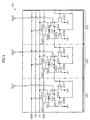
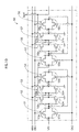
- circuits included in the regions 10 and 20 are shown as blocks. In practice, however, functional device units included in the regions 10 and 20 are densely formed on the Si substrate 31.
- each of the pixels 11 to 16 accumulates the signal charge generated by the photoelectric conversion.
- the signal charge is amplified and output.
- circuits 21 to 24 included in the drive circuit region 20 the following describes the circuit structure of the horizontal shift resistor 23, with reference to FIG.3.
- the drain region of the output transistor 2322 included in the 2 nd stage 232 is connected with a signal line for a drive pulse V2.
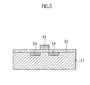
- MOS type imaging apparatus 1 pertaining to the embodiment of the present invention is characterized in that all the transistors included in both the imaging region 10 and the drive circuit region 20 are n-channel MOS type transistors. The following describes the device structure of the transistors with reference to FIG.5.
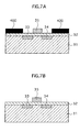
- the four steps for removing resists namely steps 3, 6, 11 and 14 damages the surface of the Si substrate 61 on which the photodiode unit is to be formed, and this damage becomes the cause of the leakage current during the driving operation.
- This leakage current is to be added to the signal generated by the photoelectric conversion, resulting in the deterioration of the image quality caused by an increase of pixel defects.
- the manufacturing method pertaining to the embodiment suppresses the 1/f noise in the amplification unit caused by a defect at a bottom part of the gate electrode 35, a leakage current in the amplification unit caused by damage of the gate insulator 32 on both sides of the gate electrode 35, and a leakage current in the photodiode unit caused by a defect of the Si substrate 31 at a bottom part of the photodiode unit.
- the leakage current can be greatly suppressed when the gate insulator 32 is a thin film of which the thickness is not more than 20 (nm) as well. This shows that the MOS type imaging apparatus 1, in which all the transistors are formed with n-channel MOS type transistors, has advantages.
Landscapes
- Engineering & Computer Science (AREA)
- Multimedia (AREA)
- Signal Processing (AREA)
- Solid State Image Pick-Up Elements (AREA)
- Transforming Light Signals Into Electric Signals (AREA)
Applications Claiming Priority (1)
| Application Number | Priority Date | Filing Date | Title |
|---|---|---|---|
| PCT/JP2002/009324 WO2004025732A1 (ja) | 2002-09-12 | 2002-09-12 | 固体撮像装置およびその製造方法 |
Publications (2)
| Publication Number | Publication Date |
|---|---|
| EP1542285A1 true EP1542285A1 (de) | 2005-06-15 |
| EP1542285A4 EP1542285A4 (de) | 2007-02-28 |
Family
ID=31986091
Family Applications (1)
| Application Number | Title | Priority Date | Filing Date |
|---|---|---|---|
| EP02807808A Withdrawn EP1542285A4 (de) | 2002-09-12 | 2002-09-12 | Rührenlose bildaufnahmeeinrichtung und herstellungsverfahren dafür |
Country Status (6)
| Country | Link |
|---|---|
| US (1) | US7352020B2 (de) |
| EP (1) | EP1542285A4 (de) |
| JP (1) | JPWO2004025732A1 (de) |
| CN (1) | CN100431160C (de) |
| TW (1) | TWI223444B (de) |
| WO (1) | WO2004025732A1 (de) |
Cited By (1)
| Publication number | Priority date | Publication date | Assignee | Title |
|---|---|---|---|---|
| EP1755159A3 (de) * | 2005-08-16 | 2008-02-20 | Matsushita Electric Industrial Co., Ltd. | Halbleiterbauelement |
Families Citing this family (22)
| Publication number | Priority date | Publication date | Assignee | Title |
|---|---|---|---|---|
| US7009663B2 (en) * | 2003-12-17 | 2006-03-07 | Planar Systems, Inc. | Integrated optical light sensitive active matrix liquid crystal display |
| US7408598B2 (en) | 2002-02-20 | 2008-08-05 | Planar Systems, Inc. | Light sensitive display with selected interval of light sensitive elements |
| US7053967B2 (en) * | 2002-05-23 | 2006-05-30 | Planar Systems, Inc. | Light sensitive display |
| US20080048995A1 (en) * | 2003-02-20 | 2008-02-28 | Planar Systems, Inc. | Light sensitive display |
| US20080084374A1 (en) * | 2003-02-20 | 2008-04-10 | Planar Systems, Inc. | Light sensitive display |
| ES2298485T3 (es) * | 2003-11-21 | 2008-05-16 | Carestream Health, Inc. | Aparato de radiologia dental. |
| US7773139B2 (en) * | 2004-04-16 | 2010-08-10 | Apple Inc. | Image sensor with photosensitive thin film transistors |
| JP2006294871A (ja) * | 2005-04-11 | 2006-10-26 | Matsushita Electric Ind Co Ltd | 固体撮像装置 |
| US20070109239A1 (en) * | 2005-11-14 | 2007-05-17 | Den Boer Willem | Integrated light sensitive liquid crystal display |
| US9310923B2 (en) | 2010-12-03 | 2016-04-12 | Apple Inc. | Input device for touch sensitive devices |
| US9329703B2 (en) | 2011-06-22 | 2016-05-03 | Apple Inc. | Intelligent stylus |
| US8638320B2 (en) | 2011-06-22 | 2014-01-28 | Apple Inc. | Stylus orientation detection |
| US8928635B2 (en) | 2011-06-22 | 2015-01-06 | Apple Inc. | Active stylus |
| US9652090B2 (en) | 2012-07-27 | 2017-05-16 | Apple Inc. | Device for digital communication through capacitive coupling |
| US9557845B2 (en) | 2012-07-27 | 2017-01-31 | Apple Inc. | Input device for and method of communication with capacitive devices through frequency variation |
| US9176604B2 (en) | 2012-07-27 | 2015-11-03 | Apple Inc. | Stylus device |
| US10048775B2 (en) | 2013-03-14 | 2018-08-14 | Apple Inc. | Stylus detection and demodulation |
| WO2014171316A1 (ja) * | 2013-04-18 | 2014-10-23 | オリンパスメディカルシステムズ株式会社 | 撮像素子、撮像装置および内視鏡システム |
| US9939935B2 (en) | 2013-07-31 | 2018-04-10 | Apple Inc. | Scan engine for touch controller architecture |
| US10061450B2 (en) | 2014-12-04 | 2018-08-28 | Apple Inc. | Coarse scan and targeted active mode scan for touch |
| US10474277B2 (en) | 2016-05-31 | 2019-11-12 | Apple Inc. | Position-based stylus communication |
| US12153764B1 (en) | 2020-09-25 | 2024-11-26 | Apple Inc. | Stylus with receive architecture for position determination |
Family Cites Families (19)
| Publication number | Priority date | Publication date | Assignee | Title |
|---|---|---|---|---|
| JP2634409B2 (ja) * | 1987-04-01 | 1997-07-23 | オリンパス光学工業株式会社 | 焦点検出用光電変換装置および焦点検出用光電変換装置の制御方法 |
| JPH05275690A (ja) | 1992-03-27 | 1993-10-22 | Toshiba Corp | 半導体装置 |
| JPH08213595A (ja) * | 1994-09-13 | 1996-08-20 | Toshiba Corp | 半導体装置 |
| US5990516A (en) * | 1994-09-13 | 1999-11-23 | Kabushiki Kaisha Toshiba | MOSFET with a thin gate insulating film |
| JPH0897292A (ja) * | 1994-09-22 | 1996-04-12 | Sharp Corp | Mosトランジスタ及び相補型mosトランジスタの製造方法 |
| JPH08148424A (ja) * | 1994-11-18 | 1996-06-07 | Yamaha Corp | 半導体装置の製造方法 |
| JPH08148677A (ja) * | 1994-11-18 | 1996-06-07 | Yamaha Corp | 半導体装置の製造方法 |
| JP3474692B2 (ja) * | 1994-12-19 | 2003-12-08 | 松下電器産業株式会社 | 半導体装置及びその製造方法 |
| KR100215759B1 (ko) * | 1994-12-19 | 1999-08-16 | 모리시타 요이치 | 반도체 장치 및 그 제조방법 |
| DE69631356T2 (de) * | 1995-08-02 | 2004-07-15 | Canon K.K. | Halbleiter-Bildaufnehmer mit gemeinsamer Ausgangsleistung |
| JP3320335B2 (ja) | 1997-05-30 | 2002-09-03 | キヤノン株式会社 | 光電変換装置及び密着型イメージセンサ |
| KR100278285B1 (ko) | 1998-02-28 | 2001-01-15 | 김영환 | 씨모스 이미지센서 및 그 제조방법 |
| JP4006111B2 (ja) * | 1998-09-28 | 2007-11-14 | キヤノン株式会社 | 固体撮像装置 |
| JP3624140B2 (ja) * | 1999-08-05 | 2005-03-02 | キヤノン株式会社 | 光電変換装置およびその製造方法、デジタルスチルカメラ又はデジタルビデオカメラ |
| JP2001339643A (ja) * | 2000-05-30 | 2001-12-07 | Nec Corp | 固体撮像装置用黒レベル発生回路及び固体撮像装置 |
| JP3558589B2 (ja) | 2000-06-14 | 2004-08-25 | Necエレクトロニクス株式会社 | Mos型イメージセンサ及びその駆動方法 |
| JP2002016839A (ja) * | 2000-06-30 | 2002-01-18 | Minolta Co Ltd | 固体撮像装置 |
| JP2002016893A (ja) | 2000-06-30 | 2002-01-18 | Sony Corp | 放送番組情報伝達方法及びデジタル放送送信機及びデジタル放送受信機及びデジタル放送記録機及びデジタル放送記録再生機 |
| JP2002133890A (ja) * | 2000-10-24 | 2002-05-10 | Alps Electric Co Ltd | シフトレジスタ |
-
2002
- 2002-09-12 CN CNB028294858A patent/CN100431160C/zh not_active Expired - Lifetime
- 2002-09-12 WO PCT/JP2002/009324 patent/WO2004025732A1/ja not_active Ceased
- 2002-09-12 EP EP02807808A patent/EP1542285A4/de not_active Withdrawn
- 2002-09-12 US US10/526,564 patent/US7352020B2/en not_active Expired - Lifetime
- 2002-09-12 JP JP2003533383A patent/JPWO2004025732A1/ja active Pending
-
2003
- 2003-06-16 TW TW092116286A patent/TWI223444B/zh not_active IP Right Cessation
Cited By (2)
| Publication number | Priority date | Publication date | Assignee | Title |
|---|---|---|---|---|
| EP1755159A3 (de) * | 2005-08-16 | 2008-02-20 | Matsushita Electric Industrial Co., Ltd. | Halbleiterbauelement |
| US7675327B2 (en) | 2005-08-16 | 2010-03-09 | Panasonic Corporation | Semiconductor device |
Also Published As
| Publication number | Publication date |
|---|---|
| TWI223444B (en) | 2004-11-01 |
| TW200404367A (en) | 2004-03-16 |
| US7352020B2 (en) | 2008-04-01 |
| WO2004025732A1 (ja) | 2004-03-25 |
| CN100431160C (zh) | 2008-11-05 |
| US20060007336A1 (en) | 2006-01-12 |
| CN1650432A (zh) | 2005-08-03 |
| EP1542285A4 (de) | 2007-02-28 |
| JPWO2004025732A1 (ja) | 2006-01-12 |
Similar Documents
| Publication | Publication Date | Title |
|---|---|---|
| US7352020B2 (en) | Solid-state image pickup device, and manufacturing method thereof | |
| US8299512B2 (en) | Solid-state imaging device | |
| EP1492334B1 (de) | Festkörper-bildaufnahmevorrichtung | |
| US7459335B2 (en) | Solid-state imaging apparatus and method for producing the same | |
| US7612819B2 (en) | CMOS image sensor and method of operating the same | |
| WO2014083730A1 (ja) | 固体撮像装置およびその駆動方法 | |
| CN113542633A (zh) | 成像装置和成像设备 | |
| CN101853851B (zh) | 电容元件及其制造方法、固态成像器件以及成像装置 | |
| JP2000201300A (ja) | 固体撮像装置、画像入力装置及び固体撮像装置のリセット方法 | |
| KR20070110767A (ko) | 고체 촬상 장치 | |
| JP2011054832A (ja) | 増幅型固体撮像素子およびその製造方法 | |
| JP2004128296A (ja) | 固体撮像素子及びその製造方法 | |
| JP4692262B2 (ja) | 固体撮像装置、固体撮像装置の駆動方法および撮像装置 | |
| KR100873280B1 (ko) | 향상된 리셋 트랜지스터를 구비한 시모스 이미지센서의단위화소 | |
| KR100464949B1 (ko) | 포토다이오드의 표면 특성을 향상시킬 수 있는 이미지센서 제조 방법 | |
| JP2001085658A (ja) | 固体撮像装置 | |
| KR20050092358A (ko) | 고체 촬상 장치 및 그 제조 방법 | |
| JPH1093868A (ja) | 固体撮像素子及びその駆動方法 | |
| JPH0697408A (ja) | 光電変換装置及びその製造方法 | |
| JP2006352169A (ja) | 固体撮像装置およびその製造方法 | |
| JP4655785B2 (ja) | 固体撮像素子の駆動方法 | |
| JPH0722611A (ja) | 電荷転送装置 | |
| KR20070021031A (ko) | 반도체 장치 |
Legal Events
| Date | Code | Title | Description |
|---|---|---|---|
| PUAI | Public reference made under article 153(3) epc to a published international application that has entered the european phase |
Free format text: ORIGINAL CODE: 0009012 |
|
| 17P | Request for examination filed |
Effective date: 20050127 |
|
| AK | Designated contracting states |
Kind code of ref document: A1 Designated state(s): DE FR GB NL |
|
| A4 | Supplementary search report drawn up and despatched |
Effective date: 20070126 |
|
| RAP1 | Party data changed (applicant data changed or rights of an application transferred) |
Owner name: PANASONIC CORPORATION |
|
| STAA | Information on the status of an ep patent application or granted ep patent |
Free format text: STATUS: THE APPLICATION HAS BEEN WITHDRAWN |
|
| 18W | Application withdrawn |
Effective date: 20090403 |