EP1545176A1 - Mehrschichtige leiterplatte und herstellungsverfahren dafür - Google Patents
Mehrschichtige leiterplatte und herstellungsverfahren dafür Download PDFInfo
- Publication number
- EP1545176A1 EP1545176A1 EP03788053A EP03788053A EP1545176A1 EP 1545176 A1 EP1545176 A1 EP 1545176A1 EP 03788053 A EP03788053 A EP 03788053A EP 03788053 A EP03788053 A EP 03788053A EP 1545176 A1 EP1545176 A1 EP 1545176A1
- Authority
- EP
- European Patent Office
- Prior art keywords
- via holes
- printed wiring
- wiring board
- multilayer printed
- double
- Prior art date
- Legal status (The legal status is an assumption and is not a legal conclusion. Google has not performed a legal analysis and makes no representation as to the accuracy of the status listed.)
- Withdrawn
Links
Images


Classifications
-
- H—ELECTRICITY
- H05—ELECTRIC TECHNIQUES NOT OTHERWISE PROVIDED FOR
- H05K—PRINTED CIRCUITS; CASINGS OR CONSTRUCTIONAL DETAILS OF ELECTRIC APPARATUS; MANUFACTURE OF ASSEMBLAGES OF ELECTRICAL COMPONENTS
- H05K3/00—Apparatus or processes for manufacturing printed circuits
- H05K3/46—Manufacturing multilayer circuits
- H05K3/4611—Manufacturing multilayer circuits by laminating two or more circuit boards
- H05K3/4614—Manufacturing multilayer circuits by laminating two or more circuit boards the electrical connections between the circuit boards being made during lamination
- H05K3/462—Manufacturing multilayer circuits by laminating two or more circuit boards the electrical connections between the circuit boards being made during lamination characterized by laminating only or mainly similar double-sided circuit boards
-
- H—ELECTRICITY
- H05—ELECTRIC TECHNIQUES NOT OTHERWISE PROVIDED FOR
- H05K—PRINTED CIRCUITS; CASINGS OR CONSTRUCTIONAL DETAILS OF ELECTRIC APPARATUS; MANUFACTURE OF ASSEMBLAGES OF ELECTRICAL COMPONENTS
- H05K3/00—Apparatus or processes for manufacturing printed circuits
- H05K3/40—Forming printed elements for providing electric connections to or between printed circuits
- H05K3/4038—Through-connections; Vertical interconnect access [VIA] connections
-
- H—ELECTRICITY
- H05—ELECTRIC TECHNIQUES NOT OTHERWISE PROVIDED FOR
- H05K—PRINTED CIRCUITS; CASINGS OR CONSTRUCTIONAL DETAILS OF ELECTRIC APPARATUS; MANUFACTURE OF ASSEMBLAGES OF ELECTRICAL COMPONENTS
- H05K2201/00—Indexing scheme relating to printed circuits covered by H05K1/00
- H05K2201/03—Conductive materials
- H05K2201/0332—Structure of the conductor
- H05K2201/0335—Layered conductors or foils
- H05K2201/0355—Metal foils
-
- H—ELECTRICITY
- H05—ELECTRIC TECHNIQUES NOT OTHERWISE PROVIDED FOR
- H05K—PRINTED CIRCUITS; CASINGS OR CONSTRUCTIONAL DETAILS OF ELECTRIC APPARATUS; MANUFACTURE OF ASSEMBLAGES OF ELECTRICAL COMPONENTS
- H05K2201/00—Indexing scheme relating to printed circuits covered by H05K1/00
- H05K2201/10—Details of components or other objects attached to or integrated in a printed circuit board
- H05K2201/10227—Other objects, e.g. metallic pieces
- H05K2201/10378—Interposers
-
- H—ELECTRICITY
- H05—ELECTRIC TECHNIQUES NOT OTHERWISE PROVIDED FOR
- H05K—PRINTED CIRCUITS; CASINGS OR CONSTRUCTIONAL DETAILS OF ELECTRIC APPARATUS; MANUFACTURE OF ASSEMBLAGES OF ELECTRICAL COMPONENTS
- H05K2203/00—Indexing scheme relating to apparatus or processes for manufacturing printed circuits covered by H05K3/00
- H05K2203/01—Tools for processing; Objects used during processing
- H05K2203/0147—Carriers and holders
- H05K2203/0156—Temporary polymeric carrier or foil, e.g. for processing or transferring
-
- H—ELECTRICITY
- H05—ELECTRIC TECHNIQUES NOT OTHERWISE PROVIDED FOR
- H05K—PRINTED CIRCUITS; CASINGS OR CONSTRUCTIONAL DETAILS OF ELECTRIC APPARATUS; MANUFACTURE OF ASSEMBLAGES OF ELECTRICAL COMPONENTS
- H05K2203/00—Indexing scheme relating to apparatus or processes for manufacturing printed circuits covered by H05K3/00
- H05K2203/07—Treatments involving liquids, e.g. plating, rinsing
- H05K2203/0703—Plating
- H05K2203/0733—Method for plating stud vias, i.e. massive vias formed by plating the bottom of a hole without plating on the walls
-
- H—ELECTRICITY
- H05—ELECTRIC TECHNIQUES NOT OTHERWISE PROVIDED FOR
- H05K—PRINTED CIRCUITS; CASINGS OR CONSTRUCTIONAL DETAILS OF ELECTRIC APPARATUS; MANUFACTURE OF ASSEMBLAGES OF ELECTRICAL COMPONENTS
- H05K2203/00—Indexing scheme relating to apparatus or processes for manufacturing printed circuits covered by H05K3/00
- H05K2203/11—Treatments characterised by their effect, e.g. heating, cooling, roughening
- H05K2203/1189—Pressing leads, bumps or a die through an insulating layer
-
- H—ELECTRICITY
- H05—ELECTRIC TECHNIQUES NOT OTHERWISE PROVIDED FOR
- H05K—PRINTED CIRCUITS; CASINGS OR CONSTRUCTIONAL DETAILS OF ELECTRIC APPARATUS; MANUFACTURE OF ASSEMBLAGES OF ELECTRICAL COMPONENTS
- H05K2203/00—Indexing scheme relating to apparatus or processes for manufacturing printed circuits covered by H05K3/00
- H05K2203/14—Related to the order of processing steps
- H05K2203/1461—Applying or finishing the circuit pattern after another process, e.g. after filling of vias with conductive paste, after making printed resistors
-
- H—ELECTRICITY
- H05—ELECTRIC TECHNIQUES NOT OTHERWISE PROVIDED FOR
- H05K—PRINTED CIRCUITS; CASINGS OR CONSTRUCTIONAL DETAILS OF ELECTRIC APPARATUS; MANUFACTURE OF ASSEMBLAGES OF ELECTRICAL COMPONENTS
- H05K3/00—Apparatus or processes for manufacturing printed circuits
- H05K3/02—Apparatus or processes for manufacturing printed circuits in which the conductive material is applied to the surface of the insulating support and is thereafter removed from such areas of the surface which are not intended for current conducting or shielding
- H05K3/06—Apparatus or processes for manufacturing printed circuits in which the conductive material is applied to the surface of the insulating support and is thereafter removed from such areas of the surface which are not intended for current conducting or shielding the conductive material being removed chemically or electrolytically, e.g. by photo-etch process
-
- H—ELECTRICITY
- H05—ELECTRIC TECHNIQUES NOT OTHERWISE PROVIDED FOR
- H05K—PRINTED CIRCUITS; CASINGS OR CONSTRUCTIONAL DETAILS OF ELECTRIC APPARATUS; MANUFACTURE OF ASSEMBLAGES OF ELECTRICAL COMPONENTS
- H05K3/00—Apparatus or processes for manufacturing printed circuits
- H05K3/10—Apparatus or processes for manufacturing printed circuits in which conductive material is applied to the insulating support in such a manner as to form the desired conductive pattern
- H05K3/20—Apparatus or processes for manufacturing printed circuits in which conductive material is applied to the insulating support in such a manner as to form the desired conductive pattern by affixing prefabricated conductor pattern
-
- H—ELECTRICITY
- H05—ELECTRIC TECHNIQUES NOT OTHERWISE PROVIDED FOR
- H05K—PRINTED CIRCUITS; CASINGS OR CONSTRUCTIONAL DETAILS OF ELECTRIC APPARATUS; MANUFACTURE OF ASSEMBLAGES OF ELECTRICAL COMPONENTS
- H05K3/00—Apparatus or processes for manufacturing printed circuits
- H05K3/38—Improvement of the adhesion between the insulating substrate and the metal
- H05K3/382—Improvement of the adhesion between the insulating substrate and the metal by special treatment of the metal
- H05K3/383—Improvement of the adhesion between the insulating substrate and the metal by special treatment of the metal by microetching
-
- H—ELECTRICITY
- H05—ELECTRIC TECHNIQUES NOT OTHERWISE PROVIDED FOR
- H05K—PRINTED CIRCUITS; CASINGS OR CONSTRUCTIONAL DETAILS OF ELECTRIC APPARATUS; MANUFACTURE OF ASSEMBLAGES OF ELECTRICAL COMPONENTS
- H05K3/00—Apparatus or processes for manufacturing printed circuits
- H05K3/38—Improvement of the adhesion between the insulating substrate and the metal
- H05K3/382—Improvement of the adhesion between the insulating substrate and the metal by special treatment of the metal
- H05K3/384—Improvement of the adhesion between the insulating substrate and the metal by special treatment of the metal by plating
-
- H—ELECTRICITY
- H05—ELECTRIC TECHNIQUES NOT OTHERWISE PROVIDED FOR
- H05K—PRINTED CIRCUITS; CASINGS OR CONSTRUCTIONAL DETAILS OF ELECTRIC APPARATUS; MANUFACTURE OF ASSEMBLAGES OF ELECTRICAL COMPONENTS
- H05K3/00—Apparatus or processes for manufacturing printed circuits
- H05K3/46—Manufacturing multilayer circuits
- H05K3/4611—Manufacturing multilayer circuits by laminating two or more circuit boards
- H05K3/4623—Manufacturing multilayer circuits by laminating two or more circuit boards the circuit boards having internal via connections between two or more circuit layers before lamination, e.g. double-sided circuit boards
-
- Y—GENERAL TAGGING OF NEW TECHNOLOGICAL DEVELOPMENTS; GENERAL TAGGING OF CROSS-SECTIONAL TECHNOLOGIES SPANNING OVER SEVERAL SECTIONS OF THE IPC; TECHNICAL SUBJECTS COVERED BY FORMER USPC CROSS-REFERENCE ART COLLECTIONS [XRACs] AND DIGESTS
- Y10—TECHNICAL SUBJECTS COVERED BY FORMER USPC
- Y10T—TECHNICAL SUBJECTS COVERED BY FORMER US CLASSIFICATION
- Y10T29/00—Metal working
- Y10T29/49—Method of mechanical manufacture
- Y10T29/49002—Electrical device making
- Y10T29/49117—Conductor or circuit manufacturing
- Y10T29/49124—On flat or curved insulated base, e.g., printed circuit, etc.
- Y10T29/49126—Assembling bases
-
- Y—GENERAL TAGGING OF NEW TECHNOLOGICAL DEVELOPMENTS; GENERAL TAGGING OF CROSS-SECTIONAL TECHNOLOGIES SPANNING OVER SEVERAL SECTIONS OF THE IPC; TECHNICAL SUBJECTS COVERED BY FORMER USPC CROSS-REFERENCE ART COLLECTIONS [XRACs] AND DIGESTS
- Y10—TECHNICAL SUBJECTS COVERED BY FORMER USPC
- Y10T—TECHNICAL SUBJECTS COVERED BY FORMER US CLASSIFICATION
- Y10T29/00—Metal working
- Y10T29/49—Method of mechanical manufacture
- Y10T29/49002—Electrical device making
- Y10T29/49117—Conductor or circuit manufacturing
- Y10T29/49124—On flat or curved insulated base, e.g., printed circuit, etc.
- Y10T29/49155—Manufacturing circuit on or in base
- Y10T29/49165—Manufacturing circuit on or in base by forming conductive walled aperture in base
Definitions
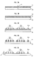
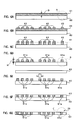
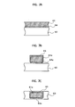
- the columnar conductors 61a which functions as the via hole 26, are coated with the low temperature diffusion metal (64a, 65). Accordingly, the following merit is obtained; i.e., the junction performance between the conductor circuits (the lower face side conductor circuit 24 and the upper face side conductor circuit 25) on the double-sided substrates 22 adjacent to the junction substrate 23 and the via holes 26 in the junction substrate 23 is increased.
Landscapes
- Engineering & Computer Science (AREA)
- Manufacturing & Machinery (AREA)
- Microelectronics & Electronic Packaging (AREA)
- Production Of Multi-Layered Print Wiring Board (AREA)
- Printing Elements For Providing Electric Connections Between Printed Circuits (AREA)
- Manufacturing Of Printed Wiring (AREA)
Applications Claiming Priority (3)
| Application Number | Priority Date | Filing Date | Title |
|---|---|---|---|
| JP2002237866 | 2002-08-19 | ||
| JP2002237866A JP2004079773A (ja) | 2002-08-19 | 2002-08-19 | 多層プリント配線板及びその製造方法 |
| PCT/JP2003/010049 WO2004017689A1 (ja) | 2002-08-19 | 2003-08-07 | 多層プリント配線板及びその製造方法 |
Publications (2)
| Publication Number | Publication Date |
|---|---|
| EP1545176A1 true EP1545176A1 (de) | 2005-06-22 |
| EP1545176A4 EP1545176A4 (de) | 2009-03-04 |
Family
ID=31884446
Family Applications (1)
| Application Number | Title | Priority Date | Filing Date |
|---|---|---|---|
| EP03788053A Withdrawn EP1545176A4 (de) | 2002-08-19 | 2003-08-07 | Mehrschichtige leiterplatte und herstellungsverfahren dafür |
Country Status (6)
| Country | Link |
|---|---|
| US (1) | US7278205B2 (de) |
| EP (1) | EP1545176A4 (de) |
| JP (1) | JP2004079773A (de) |
| CN (1) | CN1689382A (de) |
| AU (1) | AU2003254848A1 (de) |
| WO (1) | WO2004017689A1 (de) |
Families Citing this family (12)
| Publication number | Priority date | Publication date | Assignee | Title |
|---|---|---|---|---|
| US20050124197A1 (en) * | 2003-12-04 | 2005-06-09 | Matsushita Electric Industrial Co., Ltd. | Circuit board and method for manufacturing the same, semiconductor package, component built-in module and board for electronic equipment |
| JP2007059821A (ja) * | 2005-08-26 | 2007-03-08 | Shinko Electric Ind Co Ltd | 配線基板の製造方法 |
| US20160343593A1 (en) * | 2006-05-10 | 2016-11-24 | Amkor Technology, Inc. | Semiconductor package including premold and method of manufacturing the same |
| CN101472404B (zh) * | 2007-12-25 | 2011-12-07 | 富葵精密组件(深圳)有限公司 | 多层电路板及其制作方法 |
| CN102369600B (zh) * | 2009-04-02 | 2014-09-10 | 株式会社村田制作所 | 电路基板 |
| US8161637B2 (en) * | 2009-07-24 | 2012-04-24 | Ibiden Co., Ltd. | Manufacturing method for printed wiring board |
| CN103068172B (zh) * | 2012-12-26 | 2015-04-22 | 华映视讯(吴江)有限公司 | 本压印刷线路板支撑装置 |
| KR20140134479A (ko) * | 2013-05-14 | 2014-11-24 | 삼성전기주식회사 | 인쇄회로기판 |
| JP6450620B2 (ja) * | 2015-03-26 | 2019-01-09 | 東京応化工業株式会社 | 基板剥離装置および基板剥離方法 |
| JP2016219452A (ja) * | 2015-05-14 | 2016-12-22 | 富士通株式会社 | 多層基板及び多層基板の製造方法 |
| MX2020003771A (es) | 2017-09-29 | 2020-11-09 | Printpack Illinois Inc | Material de empaque con apariencia mate y brillante, y adhesivo de sellado en frio. |
| CN111491458A (zh) * | 2019-01-25 | 2020-08-04 | 鹏鼎控股(深圳)股份有限公司 | 电路板及其制作方法 |
Family Cites Families (22)
| Publication number | Priority date | Publication date | Assignee | Title |
|---|---|---|---|---|
| US3405227A (en) * | 1966-09-16 | 1968-10-08 | Control Data Corp | Multilayer universal printed circuit board |
| US3488429A (en) * | 1969-02-24 | 1970-01-06 | Gerald Boucher | Multilayer printed circuits |
| JPH04112596A (ja) * | 1990-08-31 | 1992-04-14 | Matsushita Electric Ind Co Ltd | 多層プリント配線板の製造方法 |
| JPH07106761A (ja) * | 1993-10-08 | 1995-04-21 | Hitachi Chem Co Ltd | 多層プリント配線板の製造法 |
| JPH07142863A (ja) * | 1993-11-12 | 1995-06-02 | Matsushita Electric Ind Co Ltd | 多層プリント配線板及びその製造方法 |
| JP3474913B2 (ja) | 1994-03-14 | 2003-12-08 | 株式会社東芝 | プリント配線板の製造方法 |
| JP3513827B2 (ja) * | 1996-07-01 | 2004-03-31 | 日立化成工業株式会社 | 多層プリント配線板用塑性流動シート及びそれを用いた多層プリント配線板の製造方法 |
| JPH1187921A (ja) * | 1997-09-11 | 1999-03-30 | Hitachi Chem Co Ltd | 多層配線板の製造法 |
| JPH1187922A (ja) * | 1997-09-11 | 1999-03-30 | Hitachi Chem Co Ltd | 多層配線板の製造法 |
| JPH1187923A (ja) * | 1997-09-11 | 1999-03-30 | Hitachi Chem Co Ltd | 多層配線板の製造法 |
| JP3988227B2 (ja) | 1997-12-01 | 2007-10-10 | 日立化成工業株式会社 | 半導体チップ搭載用基板の製造法および半導体装置 |
| JPH11204943A (ja) | 1998-01-08 | 1999-07-30 | Hitachi Ltd | 電子回路基板およびその製造方法 |
| JP2001111189A (ja) | 1999-10-12 | 2001-04-20 | North:Kk | 配線回路基板とその製造方法 |
| JP3981227B2 (ja) | 1999-12-28 | 2007-09-26 | テセラ・インターコネクト・マテリアルズ,インコーポレイテッド | 多層配線基板とその製造方法 |
| TW512467B (en) | 1999-10-12 | 2002-12-01 | North Kk | Wiring circuit substrate and manufacturing method therefor |
| JP2001326459A (ja) | 2000-05-16 | 2001-11-22 | North:Kk | 配線回路基板とその製造方法 |
| JP2001230551A (ja) * | 2000-02-14 | 2001-08-24 | Ibiden Co Ltd | プリント配線板並びに多層プリント配線板及びその製造方法 |
| JP3636290B2 (ja) * | 2000-03-27 | 2005-04-06 | 株式会社東芝 | プリント配線基板、及びその製造方法 |
| JP4322402B2 (ja) * | 2000-06-22 | 2009-09-02 | 大日本印刷株式会社 | プリント配線基板及びその製造方法 |
| JP2002050870A (ja) * | 2000-08-01 | 2002-02-15 | Hitachi Chem Co Ltd | 接続基板とその接続基板を用いた多層配線板と半導体パッケージ用基板と半導体パッケージ並びに接続基板の製造方法とその方法を用いた多層配線板の製造方法と半導体パッケージ用基板の製造方法と半導体パッケージの製造方法 |
| JP3769587B2 (ja) | 2000-11-01 | 2006-04-26 | 株式会社ノース | 配線回路用部材とその製造方法と多層配線回路基板と半導体集積回路装置 |
| JP2002190672A (ja) * | 2000-12-19 | 2002-07-05 | Hitachi Metals Ltd | ビルドアップコア基板、ビルドアップ配線基板、及びその製造方法 |
-
2002
- 2002-08-19 JP JP2002237866A patent/JP2004079773A/ja active Pending
-
2003
- 2003-08-07 EP EP03788053A patent/EP1545176A4/de not_active Withdrawn
- 2003-08-07 CN CN03823880.2A patent/CN1689382A/zh active Pending
- 2003-08-07 US US10/525,037 patent/US7278205B2/en not_active Expired - Fee Related
- 2003-08-07 AU AU2003254848A patent/AU2003254848A1/en not_active Abandoned
- 2003-08-07 WO PCT/JP2003/010049 patent/WO2004017689A1/ja not_active Ceased
Also Published As
| Publication number | Publication date |
|---|---|
| CN1689382A (zh) | 2005-10-26 |
| US7278205B2 (en) | 2007-10-09 |
| EP1545176A4 (de) | 2009-03-04 |
| US20060016620A1 (en) | 2006-01-26 |
| WO2004017689A1 (ja) | 2004-02-26 |
| AU2003254848A1 (en) | 2004-03-03 |
| JP2004079773A (ja) | 2004-03-11 |
Similar Documents
| Publication | Publication Date | Title |
|---|---|---|
| CN1115083C (zh) | 印刷电路板的制造方法和制成印刷电路板 | |
| US7937833B2 (en) | Method of manufacturing circuit board | |
| JP2874329B2 (ja) | 多層印刷配線板の製造方法 | |
| JP2008109140A (ja) | 回路基板及びその製造方法 | |
| US7278205B2 (en) | Multilayer printed wiring board and production method therefor | |
| US11310922B2 (en) | Board-to-board connecting structure and method for manufacturing the same | |
| JPH11186698A (ja) | 回路基板の製造方法および回路基板 | |
| GB2294363A (en) | Flexible multi-layered wiring board | |
| KR100993342B1 (ko) | 인쇄회로기판 및 그 제조방법 | |
| CN103379749A (zh) | 多层电路板及其制作方法 | |
| KR100832650B1 (ko) | 다층 인쇄회로기판 및 그 제조 방법 | |
| KR100701353B1 (ko) | 다층 인쇄 회로 기판 및 그 제조 방법 | |
| US20070029109A1 (en) | Multilayer printed wiring board and production method therefor | |
| JP3705370B2 (ja) | 多層プリント配線板の製造方法 | |
| US6492007B1 (en) | Multi-layer printed circuit bare board enabling higher density wiring and a method of manufacturing the same | |
| JP2000323841A (ja) | 多層回路基板とその製造方法 | |
| KR100441253B1 (ko) | 범프를 이용한 다층인쇄회로기판의 제조방법 | |
| JPH1174640A (ja) | プリント配線基板の製造方法 | |
| EP0572232A2 (de) | Mehrschichtige Leiterplatte und Verfahren zu ihrer Herstellung | |
| JP2004214393A (ja) | 多層配線基板の製造方法 | |
| JP4160813B2 (ja) | 多層回路基板の製造法 | |
| JP2000133943A (ja) | 多層基板の製造方法 | |
| JP3179564B2 (ja) | 多層プリント配線板およびその製造方法 | |
| JP3238901B2 (ja) | 多層プリント配線基板およびその製造方法 | |
| JPS63137498A (ja) | スル−ホ−ルプリント板の製法 |
Legal Events
| Date | Code | Title | Description |
|---|---|---|---|
| PUAI | Public reference made under article 153(3) epc to a published international application that has entered the european phase |
Free format text: ORIGINAL CODE: 0009012 |
|
| 17P | Request for examination filed |
Effective date: 20050216 |
|
| AK | Designated contracting states |
Kind code of ref document: A1 Designated state(s): AT BE BG CH CY CZ DE DK EE ES FI FR GB GR HU IE IT LI LU MC NL PT RO SE SI SK TR |
|
| AX | Request for extension of the european patent |
Extension state: AL LT LV MK |
|
| DAX | Request for extension of the european patent (deleted) | ||
| A4 | Supplementary search report drawn up and despatched |
Effective date: 20090129 |
|
| STAA | Information on the status of an ep patent application or granted ep patent |
Free format text: STATUS: THE APPLICATION IS DEEMED TO BE WITHDRAWN |
|
| 18D | Application deemed to be withdrawn |
Effective date: 20090428 |