EP1633521B1 - Film de tensioactif utilise dans un usinage laser - Google Patents
Film de tensioactif utilise dans un usinage laser Download PDFInfo
- Publication number
- EP1633521B1 EP1633521B1 EP04739567A EP04739567A EP1633521B1 EP 1633521 B1 EP1633521 B1 EP 1633521B1 EP 04739567 A EP04739567 A EP 04739567A EP 04739567 A EP04739567 A EP 04739567A EP 1633521 B1 EP1633521 B1 EP 1633521B1
- Authority
- EP
- European Patent Office
- Prior art keywords
- wafer
- surfactant
- laser machining
- laser
- film
- Prior art date
- Legal status (The legal status is an assumption and is not a legal conclusion. Google has not performed a legal analysis and makes no representation as to the accuracy of the status listed.)
- Expired - Lifetime
Links
Images


Classifications
-
- B—PERFORMING OPERATIONS; TRANSPORTING
- B23—MACHINE TOOLS; METAL-WORKING NOT OTHERWISE PROVIDED FOR
- B23K—SOLDERING OR UNSOLDERING; WELDING; CLADDING OR PLATING BY SOLDERING OR WELDING; CUTTING BY APPLYING HEAT LOCALLY, e.g. FLAME CUTTING; WORKING BY LASER BEAM
- B23K26/00—Working by laser beam, e.g. welding, cutting or boring
- B23K26/18—Working by laser beam, e.g. welding, cutting or boring using absorbing layers on the workpiece, e.g. for marking or protecting purposes
-
- B—PERFORMING OPERATIONS; TRANSPORTING
- B23—MACHINE TOOLS; METAL-WORKING NOT OTHERWISE PROVIDED FOR
- B23K—SOLDERING OR UNSOLDERING; WELDING; CLADDING OR PLATING BY SOLDERING OR WELDING; CUTTING BY APPLYING HEAT LOCALLY, e.g. FLAME CUTTING; WORKING BY LASER BEAM
- B23K26/00—Working by laser beam, e.g. welding, cutting or boring
- B23K26/16—Removal of by-products, e.g. particles or vapours produced during treatment of a workpiece
-
- Y—GENERAL TAGGING OF NEW TECHNOLOGICAL DEVELOPMENTS; GENERAL TAGGING OF CROSS-SECTIONAL TECHNOLOGIES SPANNING OVER SEVERAL SECTIONS OF THE IPC; TECHNICAL SUBJECTS COVERED BY FORMER USPC CROSS-REFERENCE ART COLLECTIONS [XRACs] AND DIGESTS
- Y10—TECHNICAL SUBJECTS COVERED BY FORMER USPC
- Y10T—TECHNICAL SUBJECTS COVERED BY FORMER US CLASSIFICATION
- Y10T428/00—Stock material or miscellaneous articles
- Y10T428/26—Web or sheet containing structurally defined element or component, the element or component having a specified physical dimension
- Y10T428/263—Coating layer not in excess of 5 mils thick or equivalent
- Y10T428/264—Up to 3 mils
- Y10T428/265—1 mil or less
-
- Y—GENERAL TAGGING OF NEW TECHNOLOGICAL DEVELOPMENTS; GENERAL TAGGING OF CROSS-SECTIONAL TECHNOLOGIES SPANNING OVER SEVERAL SECTIONS OF THE IPC; TECHNICAL SUBJECTS COVERED BY FORMER USPC CROSS-REFERENCE ART COLLECTIONS [XRACs] AND DIGESTS
- Y10—TECHNICAL SUBJECTS COVERED BY FORMER USPC
- Y10T—TECHNICAL SUBJECTS COVERED BY FORMER US CLASSIFICATION
- Y10T428/00—Stock material or miscellaneous articles
- Y10T428/31504—Composite [nonstructural laminate]
Definitions
- This invention relates to use of a surfactant film to reduce adhesion of laser machining debris to a workpiece being machined.
- some material removed from a machining zone is deposited on a surface of the wafer substrate on which machining is being carried out, for example as debris at the edge of a laser cut.
- Material ejected from the machining zone during laser machining is in a molten or gaseous form and adheres to the surface of the wafer substrate upon cooling during, and subsequent to, machining.
- adherent debris may, for example, damage thermally-sensitive electronic circuitry on the surface of the wafer substrate as the debris cools upon contact with the surface and re-solidifies.
- Such re-solidified debris is difficult to remove from the surface of the wafer substrate using conventional wafer cleaning techniques due to its adherent nature.
- US 2003/052098 discloses a method of cutting a substrate, in particular a glass substrate to be used in a liquid crystal display, using a coolant rapidly to cool a heated portion of the substrate which may be heated by a scribing laser beam.
- the coolant may be water containing a surfactant to cause the water to spread over a larger area.
- US 6,048,671 discloses ultra-fine micro-fabrication using nanoparticles as shielding members.
- the micro-particles are dispersed on the surface in a solvent stirred with a surfactant to obtain uniform dispersion. Subsequently the solvent is evaporated to leave only the micro-particles on the surface. The surface is then irradiated with an atomic beam with the micro-particles forming an etch mask.
- the surfactant is dispensed in a pre-wash of the workpiece.
- the method includes a further step of at least partially drying the surfactant film before laser machining the workpiece.
- the step of dispensing a surfactant comprises dispensing a surfactant onto surfaces of a plurality of workpieces in a batch process before the workpieces are laser machined.
- the step of dispensing a surfactant comprises dispensing a surfactant which is soluble in a solvent in which the surface of the workpiece is insoluble and wherein the step of removing the surfactant film comprises dissolving the surfactant film in the solvent.
- the solvent is water.
- the step of laser machining the workpiece comprises laser machining a multilayer workpiece.
- the multilayer workpiece comprises a semiconductor wafer and associated layers forming an active region of the wafer.
- the step of dispensing the surfactant comprises spray depositing the surfactant film on the surface.
- the step of dispensing the surfactant comprises knife-edge depositing the surfactant film on the surface.
- the step of dispensing the surfactant comprises roller depositing the surfactant film on the surface.
- the step of dispensing the surfactant comprises immersing the surface of the workpiece in a surfactant solution.
- the step of dispensing the surfactant comprises dipping a batch of wafers to be machined into a surfactant solution.
- the step of dispensing the surfactant comprises dispensing an anionic, non-ionic or amphoteric surfactant.
- the step of dispensing the surfactant comprises coating the surface with a surfactant film having a sufficiently high degree of wetting to wet substantially all the surface.
- the step of laser machining includes optimisation of machining parameters and such optimisation includes seeking to minimise adherence of debris to the surfactant film.
- the step of removing the surfactant film comprises a spin-rinse-dry process.
- the step of laser machining comprises laser scribing the workpiece and the step of removing the surfactant film comprises at least partially removing the thin film of surfactant and any debris with a coolant used in a subsequent dicing step using a dicing saw.
- the step of laser machining comprises providing a gas environment for the laser machining for reducing solid debris created in the laser machining step.
- the step of dispensing the surfactant comprises coating the surface with a surfactant dissolved or suspended in a liquid carrier and evaporating the liquid carrier from the surface.
- the step of dispensing the surfactant to form a thin film of surfactant comprises the step of acquiring an image of the film of surfactant on the workpiece and comparing the image with a reference image of a workpiece with an optimum thin film of surfactant and where the image is not sufficiently comparable with the reference image washing the surfactant film form the workpiece and redispensing surfactant on the surface of the workpiece.
- the step of comparing the image with a reference image includes comparing the image with at least one of a second reference image of a workpiece with an excess of surfactant on a surface and a third reference image of a workpiece with insufficient surfactant on a surface to determine whether the thin film of surfactant is excessive or insufficient respectively.
- the step of dispensing a surfactant onto a surface of the workpiece comprises a step of using a camera and associated hardware and software to align a wafer on an xy table with machine coordinates of a laser apparatus with which the wafer is to be machined, or with a laser of the laser apparatus, before the surfactant is dispensed on the wafer, such that the surfactant is dispensed on the wafer on the xy table after the wafer has been clamped in position thereon.
- the step of dispensing a surfactant comprises the steps of: removing a wafer from wafer carrier means; transporting the wafer to a surfactant dispensing station and coating the surface of the wafer with a surfactant film to form a coated wafer; and the step of laser machining comprises transporting the coated wafer to a laser machining station and laser machining the coated wafer to form a machined coated wafer such that debris from the laser machining is deposited on the surfactant film; and the step of removing the surfactant film comprises the steps of transporting the machined coated wafer to a surfactant removal station and removing the surfactant film and the debris deposited thereon to form an uncoated machined wafer.
- the surfactant dispensing means comprises pre-washing means.
- the surfactant film removal means comprises spin-rinse-dry means
- the pre-washing means and the post-washing means are a same washing means.
- the laser machining apparatus is arranged for at least one of laser scribing, laser dicing and laser via drilling the workpiece.
- the laser machining apparatus further comprises drying means arranged at least partially to dry the surface subsequent to coating the surface.
- the laser machining apparatus further comprises imaging means for obtaining an image of the surfactant film on the surface of the workpiece and image comparison means for comparing the image with a least one reference image for determining whether the thin film of the surfactant is sufficiently optimised for laser machining.
- the surfactant dispensing means comprises a surfactant dispensing station for coating a surface of a workpiece to be laser machined with the surfactant film for reducing adherence to the surface of debris produced during laser machining by producing a coated workpiece;
- the laser machining apparatus further comprises a laser machining station for machining the coated workpiece;
- the surfactant removal means comprise a surfactant film removal station for removing the surfactant film subsequent to laser machining together with any debris from the laser machining deposited thereon; and the laser machining apparatus further comprises transport means for transporting the workpiece from the surfactant dispensing station to the laser machining station and from the laser machining station to the surfactant film coating removal station.
- the surfactant film is removable subsequent to laser machining without significantly damaging the at least one surface.
- the surfactant film is not more than 10 micron thick.
- the surfactant film is an anionic, ionic or amphoteric surfactant film.
- the thin film of surfactant is less than 10 microns thick.
- the thin film of surfactant 11 has a sufficiently high degree of wetability to ensure that the film uniformly wets the wafer surface and remains on the wafer surface during machining.
- the surfactant film is applied in a pre-wash of the wafer.
- the surface is at least partially dried after the thin flm of surfactant has been applied and before laser machining.
- the wafer substrate is machined while the surface is still wet.
- the wafers may be pre-deposited, for example hours or days before laser machining, and then fed into a laser machining apparatus in a normal manner.
- a full boat of wafers may be coated by a dipping process or alternative batch process in advance of insertion into the laser machining apparatus.
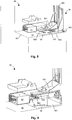
- Laser beam parameters such as wavelength, laser pulse energy, laser repetition rate and scanning velocity of the laser beam 14 over the wafer substrate 12, determine a nature of the debris 15 produced during laser machining.
- a combination of parameters, such as wavelength, laser pulse energy, laser repetition rate and scanning velocity of the laser beam 14 over the wafer substrate 12, are preferably chosen, subject to other constraints, to produce debris 15 that has low adherence to the thin film of surfactant upon re-solidification and is therefore more easily removed in a wash process. That is, the presence of the thin film of surfactant on the wafer surface after a pre-wash step reduces the surface adhesive properties thus permitting easier removal of the laser-machined debris.
- molten and gaseous material 15 is ejected from the laser machining site 13 during laser machining. Such material moves back toward the wafer surface both during and after laser machining and is deposited on the thin film of surfactant 11 as re-solidified material 151, as shown in Figure 1(b) .
- the surfactant film reduces adherence of the debris to the workpiece, easing subsequent removal of debris from the workpiece. This differs from a known protective coating which physically prevents debris coming into contact with the surface of the wafer by acting as a barrier. In the case of the thin film of surfactant of the invention, the process of physically or chemically bonding debris or laser re-deposited material to the wafer is prevented.
- the surfactant acts as an "anti-fluxing" agent.
- This may be understood as a reverse process to that of a solder flux in which a chemical is added to allow metal to bond better to a metal pad, for example, by chemically stimulating the bonding process at elevated temperature.
- the wafer substrate 12 is washed using a conventional wash for semiconductor substrates, such as a spin-rinse-dry process with water, and both the thin film of surfactant 11 and re-solidified debris 151 are removed from the wafer surface, leaving the surface clean and undamaged, as shown in Figure 1(c) .
- a conventional wash for semiconductor substrates such as a spin-rinse-dry process with water
- laser machining is performed in an active gas environment or in a gas environment where photo-dissociation produces active radicals.
- Laser machining in an active gas environment can change the chemical nature of debris produced.
- a chemical reaction between the active gas and the debris 15 while in a molten state can result in removal of debris in gaseous form, with consequentially reduced deposition of solid debris 151 around the laser machining site 13.
- FIG. 2 which shows a nozzle 21, for emitting a jet of liquid surfactant, mounted above the wafer substrate 12.
- the wafer substrate 12 is rotated in the sense of arcuate arrow 22 and the nozzle 21 is translated in the plane of the wafer in direction of double arrow headed line 23 to ensure complete wafer coverage with the liquid surfactant.
- Figure 3 illustrates liquid surfactant dispensing through a linear dispensing head 31 via a linear knife edge type nozzle 311 that is at least a same length as a diameter of the wafer substrate 12.
- a roller 41 may be used to dispense surfactant on the wafer substrate 12 by rotation in the sense of arcuate arrow 44 and translation over the wafer surface in the direction of double arrow headed line 43.
- the wafer substrate 12 may be rotated in the sense of arcuate arrow 42.
- a wafer may be placed on an XY table, the wafer aligned and the surfactant solution deposited on the wafer prior to machining, that is the deposition head or mechanism is used on the XY table after the wafer has been clamped in position.
- the surface is at least partially dried subsequent to pre-washing and before laser machining since the thin film 11 is also efficient in reducing the adhesive properties of the substrate 12 when a primary solvent carrying the surfactant has evaporated or where the thin layer is formed by a phase change or congealing of a deposited surfactant solution.
- the surface may be laser machined with a wet surfactant film.
- the thin film of surfactant 11 may be deposited in a batch process.
- the wafers are pre-deposited, for example hours or days before laser machining, and then fed into a laser machining apparatus in a normal manner.
- a full boat of wafers may be coated by a dipping process in advance of insertion into the laser machining apparatus.
- a laser machining apparatus 50 for carrying out the steps of the method of the invention is illustrated schematically in Figures 5 to 9 .
- a cassette holder 51 for holding a stack of spaced-apart wafers 12, is located on a table or frame 52 at a first end 521 thereof.
- the cassette holder 51 is generally cuboid with open opposed vertical ends transverse to a longitudinal axis of the table or frame 52, to provide access to wafers 12 stacked therein.
- the cassette holder 51 Spaced generally vertically above, in use, the cassette holder 51 is a surfactant dispensing (pre-wash) station 53 having a roller 531 with an axle 532 transverse to the longitudinal axis of the table or frame 52 and parallel to a plane defined by a surface of the table or frame 52.
- the roller 531 is partially immersed in a bath 533 for containing surfactant solution to be deposited on a surface of the wafer substrate 12.
- the apparatus preferably includes a drying station, not shown, possibly combined with the surfactant dispensing station, for drying the surface subsequent to pre-washing and before laser machining.
- a drying station possibly combined with the surfactant dispensing station, for drying the surface subsequent to pre-washing and before laser machining.
- An infrared lamp, an oven or a warm air jet are examples of suitable means of drying the surface.
- a laser machining head 54 is located offset from the table or frame 52 corresponding to a position on the table or frame 52 between the cassette holder 51 and a second end 522 of the table or frame 52 opposed to the first end 521.
- the laser machining head 54 has a vertical access end 541 open for loading wafers to be machined and unloading machined wafers, which is most proximate the table or frame 52 and parallel to the longitudinal axis thereof.
- a coating removal bath 55 is sunk in a well 551 in the table or frame 52 between the cassette holder 51 and the second end 522 of the table or frame 52 and proximate the access end 541 of the laser machining head 54.
- a same bath may be used for pre-washing to deposit the surfactant on the surface and for post-washing to remove the surfactant film and debris from the surface.
- a robot 56 located at the second end 522 of the table or frame 52, proximate the well 551, is a robot 56 having a substantially horizontal, in use, platform 561, vertically movable with respect to the table or frame 52 above the well 551 on vertical, in use, guide rails 560 substantially perpendicular to the surface of the table or frame 52.
- An end effector carrier 562 is rotatably suspended from the platform 561 by a vertical axle 563 passing through the platform 561 for rotation of the end effector carrier 562 with respect to the platform 561 and substantially parallel to the surface of the table or frame 52.
- An end effector 564 is slideably mounted on the end effector carrier 562 for movement with respect to the end effector carrier 562 parallel to a longitudinal axis thereof between an extended position and a retracted position.
- Figures 5 to 9 illustrate, in sequence, use of the laser machining apparatus to perform the process steps of a complete cycle of the method of the invention of pre-washing a substrate to form a thin film of surfactant on the substrate, laser machining the substrate and removing the thin film surfactant from the substrate.
- the cassette holder 51 is loaded with wafer substrates 12 to be laser machined.
- the wafer substrates may optionally be mounted on respective tape frames 121.
- a selected wafer substrate 12 is removed from the wafer cassette holder 51, as shown in Figure 5 , using the end-effector 564 attached to the robot 56, by locating the platform 561 at a suitable height above the surface of the table or frame 52 to extend the end effector 564, with a longitudinal axis of the end effector carrier 562 parallel to the longitudinal axis of the table or frame 52, towards the cassette holder 51 for the end effector 564 to engage the selected wafer substrate 12 in the cassette holder and by retracting the end effector 564 with the selected wafer substrate 12 held by the end effector 564.
- a slide mechanism may be used instead of the robot.
- the wafer substrate 12, held by the end effector 564, is transported vertically away from the surface of the table or frame 52 by the robot to the pre-wash station 53.
- the end effector 564 is extended such that a lower, in use, surface of the wafer substrate 12 to be machined engages the roller 531, as shown in Figure 6 .
- the roller 531 is rotated about the roller axle 532 as the end effector 564 moves the wafer substrate 12 over the roller 531 to wash the lower surface of the wafer substrate 12 in a surfactant solution from the bath 533.
- Alternative dispensing tools such as a nozzle or knife edge dispenser may alternatively be used, optionally with the wafer being rotated with respect to the dispensing tool during pre-washing.
- the wafer substrate 12 When pre-washed, the wafer substrate 12 is removed from the prewash station 53 by retracting the end effector 564 and lowering the platform 561 and end effector 564 towards the surface of the table or frame 52 to a suitable distance from the surface to position the wafer substrate 12 at a machining position in the laser machining head 54. As shown in figure 7 , the end effector carrier is rotated through substantially 90° about the axle 563 thereof towards the laser machining head 54. The end effector 564 is extended to pass the pre-washed wafer substrate 12 through the laser machining head access 541 for laser machining of the pre-washed wafer substrate 12, from the lower, in use, pre-washed surface thereof. During laser machining, debris which would otherwise be deposited on the lower surface of the wafer substrate 12 is deposited on the thin film of surfactant.
- the wafer substrate 12 is removed from the laser machining head 54 by retracting the end effector 564 and rotating the end effector carrier 562 through substantially 90° in an opposite sense to that in which the carrier was rotated to load the substrate into the laser machining head and lowering the platform 561 in the direction of the surface of the table or frame 52 to immerse the machined substrate in the washing system 55. Both the surfactant layer and debris are removed during a wash cycle.
- the wafer substrate 12 is then removed from the washing system 55 by moving the platform 561 away from the surface of the table or frame 52 to a distance from the surface sufficient to re-insert the machined and washed wafer substrate 12 into the cassette holder 51.
- the end effector 564 is extended to insert the wafer substrate 12 in the cassette holder 51 and the wafer substrate 12 released from the end effector 564 in the cassette holder 51.
- the wafer substrate 12 is returned to the wafer cassette holder 51 immediately after laser machining and remains therein until all wafers 12 in the cassette holder 51 have been sequentially pre-washed and laser machined.
- the entire batch of wafers in the cassette is then loaded into the washing system 55 and all wafers 12 are washed in one wash cycle, thus reducing machine cycling time for a wafer batch.
- throughput of the system may be improved through the use of a buffer.
- wafers are sequentially passed through the dispense and dry step and fed into a buffer.
- the buffer is unloaded sequentially to feed wafers into the XY table where machining occurs and following machining the wafers are unloaded to the washer.
- Optimisation of the number of wafers in the buffer will depend on the number of wafers in a cassette as well as deposition and dry times, handling times, machining time and wash times. A correctly optimised buffer significantly increases throughput.
- the camera system used to perform wafer alignment is used to detect and confirm the presence of surfactant on the wafer before machining. This for example may be achieved through use of an ideal or "golden" image of an ideal wafer. In further refinement, excess or insufficient surfactant may also be detected through comparison with images of workpieces with excess or insufficient surfactant. This method may be used as an inline control system to prevent machining of wafers which have, through operator error or machine fault, not received an amount of surfactant sufficiently close to an optimum amount.
- the method of the present invention is to laser machine semiconductor substrates, for example, that have been pre-washed in a surfactant solution in order to reduce the adhesive properties of a surface of the substrate upon which laser machined debris will collect.
- This thin film of surfactant, and the debris deposited on the thin film of surfactant, are removed subsequent to laser machining of the substrate thus leaving the wafer surface free of debris and undamaged.
- This invention is applicable to, for example, laser dicing, laser scribing and laser via drilling in single substrate and multi-layer substrate materials consisting of layers such as plastic, dielectric, glass, metal and semiconductor materials.
- the invention provides the advantages that the thin film of surfactant is easier to remove than known protective plastics films and the surfactant is compatible with known processing being similar to that used as a wetability agent in mechanical sawing of wafers.
- a dicing process or dicing saw is used in subsequent processing and the sawing process uses water as a coolant or lubricant, that water may also be used to remove the thin film of surfactant.
Landscapes
- Engineering & Computer Science (AREA)
- Physics & Mathematics (AREA)
- Optics & Photonics (AREA)
- Plasma & Fusion (AREA)
- Mechanical Engineering (AREA)
- Laser Beam Processing (AREA)
- Dicing (AREA)
- Cleaning Or Drying Semiconductors (AREA)
Claims (33)
- Procédé de réduction des propriétés de liaison à une tranche de semi-conducteur de débris resolidifiés produits pendant l'usinage laser de la tranche (12), et de facilitation de l'enlèvement des débris de la tranche après son usinage laser, dans lequel l'usinage laser de la tranche comprend l'un d'un traçage au laser, d'un découpage au laser et d'un perçage de trous d'interconnexion au laser de la tranche, le procédécomprenant les étapes consistant à :a. avant l'usinage laser, appliquer un film de tensioactif comprenant un tensioactif dissous ou mis en suspension dans un entraîneur liquide sur une surface de la tranche à usiner au laser, le film de tensioactif ayant un degré suffisamment élevé de mouillabilité pour garantir que le film mouille de manière uniforme la surface de la tranche et reste sur la surface pendant l'usinage laser ; etb. après le revêtement de la surface de la tranche, collecter les débris sur le film de tensioactif pendant et après l'usinage laser de la tranche, dans lequel l'usinage laser est appliqué à partir de la surface sur laquelle se trouve le film de tensioactif ; etc. après la collecte des débris, enlever par lavage le film de tensioactif avec les débris collectés de la tranche dans des moyens de bain.
- Procédé selon la revendication 1, comprenant l'étape supplémentaire consistant à, après l'application du film de tensioactif et avant l'usinage laser de la tranche, évaporer l'entraîneur liquide de la surface pour fournir un film de tensioactif sec (11) sur la surface ; dans lequel l'usinage laser comprend l'étape consistant à usiner au laser la tranche à partir de la surface sur laquelle se trouve le film de tensioactif sec ; et dans lequel la collecte des débris comprend l'étape consistant à collecter les débris sur le film de tensioactif sec.
- Procédé selon la revendication 1 ou 2, dans lequel le film de tensioactif est appliqué dans un prélavage de la tranche.
- Procédé selon la revendication 2, dans lequel l'évaporation comprend l'étape consistant à sécher avec au moins l'un d'une lampe à infrarouge, d'un four et d'un jet d'air chaud.
- Procédé selon l'une quelconque des revendications précédentes, dans lequel l'application du film de tensioactif comprend l'étape consistant à appliquer le film de tensioactif sur des surfaces d'une pluralité de tranches dans un procédédiscontinu avant que les tranches ne soient usinées au laser.
- Procédé selon l'une quelconque des revendications précédentes, dans lequel l'application du film de tensioactif comprend l'étape consistant à appliquer un tensioactif qui est soluble dans un solvant dans lequel la surface de la tranche est insoluble et dans lequel l'enlèvement du film de tensioactif comprend l'étape consistant à dissoudre le film de tensioactif dans le solvant.
- Procédé selon la revendication 6, dans lequel le solvant est de l'eau.
- Procédé selon l'une quelque des revendicationsprécédentes, dans lequel l'usinage laser de la tranche comprend l'étape consistant à usiner au laser une tranche multicouche.
- Procédé selon la revendication 8, dans lequel l'usinage laser d'une tranche multicouche comprend l'étape consistant à usiner une tranche de semi-conducteur et les couches associées formant une région active de la tranche.
- Procédé selon l'une quelque des revendicationsprécédentes, dans lequel l'application du film de tensioactif comprend l'étape consistant à déposer par pulvérisationle film de tensioactif sur la surface.
- Procédé selon l'une quelconque des revendications 1 à 9, dans lequel l'application du film de tensioactif comprend l'étape consistant à appliquer au tranchant le film de tensioactif sur la surface.
- Procédé selon l'une quelconque des revendications 1 à 9, dans lequel l'application du film de tensioactif comprend l'étape consistant à appliquer au rouleau le film de tensioactif sur la surface.
- Procédé selon l'une quelconque des revendications 1 à 9, dans lequel l'application du film de tensioactif comprend l'étape consistant à immerger la surface de la tranche dans une solution de tensioactif.
- Procédé selon la revendication 13, dans lequel l'application du film de tensioactif comprend l'étape consistant à immerger un lot de tranches à usiner dans la solution de tensioactif.
- Procédé selon l'une quelconque des revendications précédentes, dans lequel l'application du film de tensioactif comprend l'étape consistant à appliquer un tensioactif anionique, non ionique ou amphotère.
- Procédé selon l'une quelconque des revendications précédentes, dans lequel l'usinage laser comprend l'étape consistant à optimiser les paramètres d'usinage et ladite optimisation comprend l'étape consistant à chercher à minimiser l'adhérence de débris (15) au film de tensioactif.
- Procédé selon l'une quelque des revendicationsprécédentes, dans lequel l'enlèvement du film de tensioactif comprend un processus d'essorage/rinçage/séchage.
- Procédé selon l'une quelconque des revendications précédentes, dans lequel l'usinage laser comprend l'étape consistant à tracer au laser la tranche et l'enlèvement du film de tensioactif comprend l'étape consistant à enlever au moins partiellement le mince film de tensioactif et tout débris avec un liquide de refroidissement utilisé dans une étape subséquente de découpage en utilisant une scie de découpage.
- Procédé selon l'une quelconque des revendications précédentes, dans lequel l'usinage laser comprend l'étape consistant à fournir un environnement gazeux pour l'usinage laser pour réduire les débris solides créés lors de l'usinage laser.
- Procédé selon l'une quelconque des revendications précédentes, dans lequel l'application du film liquide (11) comprend l'étape consistant à acquérir une image du film de tensioactif sur la tranche et à comparer l'image avec une image de référence d'une tranche avec un film mince optimum de tensioactifs et lorsque l'image n'est pas suffisamment comparable avec l'image de référence, laver la tranche et réappliquer le tensioactif sur la surface de la tranche.
- Procédé selon la revendication 20, dans lequel la comparaison de l'image à une image de référence comprend l'étape consistant à comparer l'image à au moins l'une d'une deuxième image de référence d'une tranche avec un excès de tensioactif sur une surface et à une troisième image de référence d'une tranche avec un manque de tensioactif sur une surface.
- Procédé selon l'une quelconque des revendications précédentes, dans lequel l'application du film de tensioactif sur une surface de la tranche comprend une étape consistant à utiliser une caméra et le matériel et le logiciel associés pour aligner une tranche sur une table XY avec des coordonnées d'usinage d'un appareil laser avec lequel la tranche doit être usinée, ou avec un laser de l'appareil laser, avant que le tensioactif ne soit appliqué sur la tranche, de telle sorte que le tensioactif soit appliqué sur la tranche sur la table XY après que la tranche a été fixée en position sur elle.
- Procédé selon l'une quelconque des revendications précédentes, comprenant les étapes consistant à :a. enlever une tranche (12) de moyens formant entraîneur de tranche (51) ;b. transporter la tranche jusqu'à une station d'application de tensioactif (53) et recouvrir la surface de la tranche avec un film de tensioactif (11) pour former une tranche à revêtement ;c. transporter la tranche à revêtement jusqu'à une station d'usinage laser (54) et usiner au laser la tranche à revêtement pour former une tranche à revêtement usinée de telle sorte que les débris (151) provenantde l'usinage laser sont déposés sur le film de tensioactif ; etd. transporter la tranche à revêtement usinée jusqu'à une station d'enlèvement de tensioactif (55) et enlever le film de tensioactif et les débris (151) déposés dessus pour former une tranche usinée sans revêtement.
- Appareild'usinage laser agencé pour l'un d'un traçage au laser, d'un découpage au laser et d'un perçage de trous d'interconnexion au laser d'une tranche à revêtement, caractérisé par :a. des moyens d'application de tensioactif comprenant l'un de :i. moyens de dépôt par pulvérisation comprenant une buse (21) pouvant être translatée sur un plan parallèle à la trancheet des moyens de rotation pour faire tourner la tranche en dessous de la buse ;ii. une buse à tranchant linéaire pouvant être translatée sur un plan parallèle à la trancheet des moyens de rotation pour faire tourner la tranche en dessous de la buse ;iii. qui des moyens de rouleau pouvant être translatés sur un plan parallèle à la tranche et des moyens de rotation pour faire tourner la tranche sous les moyens de rouleau ; etiv. des moyens de bain de prélavage pour l'immersion de la tranche dedansagencés pour appliquer un film de tensioactif comprenant un tensioactif dissous ou mis en suspension dans un entraîneur liquide sur une surface de la tranche (12) à usiner, le film de tensioactif ayant une mouillabilité uniforme pour recouvrir une surface de la tranche, agencés pour réduire les propriétés adhésives de surface des débris (151) déposés dessus pendant l'usinage laser par l'appareil ;b. des moyens de génération de faisceau laser et de contrôle d'environnement gazeux agencés pour réduire le dépôt solide des débris résultants produits au cours de l'usinage laser sur le film de tensioactif ;c. et des moyens d'enlèvement de film de tensioactif comprenant des moyens de bain postlavage agencés pour enlever par lavage le film de tensioactif avec les débris déposés de la surface de la tranche après l'usinage laser.
- Appareild'usinage laser selon la revendication 26, comprenant en outre des moyens de séchage agencés au moins partiellement pour évaporer l'entraîneur liquide de la surface, après l'application du film de tensioactif pour recouvrir la surface avec un tensioactif sec (11).
- Appareild'usinage laser selon la revendication 24, dans lequel les moyens d'application de tensioactif comprennent des moyens de prélavage.
- Appareild'usinage laser selon les revendications 24 à 26, dans lequel les moyens d'enlèvement de film de tensioactif comprennent des moyens d'essorage/rinçage/séchage.
- Appareild'usinage laser selon les revendications 24 à 26, dans lequel les moyens d'enlèvement de film de tensioactif comprennent des moyens de postlavage.
- Appareil d'usinage laser selon la revendication 28, dans lequel les moyens de prélavage et les moyens de postlavage sont les mêmes moyens de lavage.
- Appareild'usinage laser selon l'une quelconque des revendications 24 à 29, dans lequel les moyens d'application de tensioactif comprennent des moyens d'immersion pour le trempage par lot d'une pluralité de tranches.
- Appareild'usinage laser selon l'une quelconque des revendications 24 à 30, comprenant en outre des moyens de contrôle d'environnement gazeux pour produire un environnement gazeux pour l'usinage laser agencés pour réduire les débris solides (15) produits pendant l'usinage laser.
- Appareild'usinage laser selon l'une quelconque des revendications 24 à 31, comprenant en outre des moyens d'imagerie pour obtenir une image du film de tensioactif sur la surface de la tranche et des moyens de comparaison d'image pour comparer l'image à au moins une image de référence pour déterminer si le mince film du tensioactif est suffisamment optimisé pour l'usinage laser.
- Appareild'usinage laser selon la revendication 24, comprenant : une station d'application de tensioactif (53) pour recouvrir une surface d'une tranche (12) devant être usinée au laser avec le film de tensioactif (11) pour réduire l'adhérence à la surface des débris (15) produits pendant l'usinage laser par production d'une tranche à revêtement ; une station d'usinage laser pour usiner la tranche à revêtement ; une station d'enlèvement de film de tensioactif pour enlever le film de tensioactif (11) après l'usinage laser avec les débris (151) de l'usinage laser déposés dessus ; et des moyens de transport (560, 561, 562, 563, 564) pour transporter la tranche de la station d'application de tensioactif (53) à la station d'usinage laser (54) et de la station d'usinage laser (54) à la station d'enlèvement de revêtement de film de tensioactif (55).
Applications Claiming Priority (3)
| Application Number | Priority Date | Filing Date | Title |
|---|---|---|---|
| GB0313115A GB0313115D0 (en) | 2003-06-06 | 2003-06-06 | Laser machining using a protective coating |
| GB0400677A GB2409998B (en) | 2004-01-13 | 2004-01-13 | Laser machining using a surfactant film |
| PCT/EP2004/006001 WO2004110694A2 (fr) | 2003-06-06 | 2004-06-03 | Film de tensioactif utilise dans un usinage laser |
Publications (2)
| Publication Number | Publication Date |
|---|---|
| EP1633521A2 EP1633521A2 (fr) | 2006-03-15 |
| EP1633521B1 true EP1633521B1 (fr) | 2012-04-11 |
Family
ID=33554138
Family Applications (1)
| Application Number | Title | Priority Date | Filing Date |
|---|---|---|---|
| EP04739567A Expired - Lifetime EP1633521B1 (fr) | 2003-06-06 | 2004-06-03 | Film de tensioactif utilise dans un usinage laser |
Country Status (8)
| Country | Link |
|---|---|
| US (1) | US9242312B2 (fr) |
| EP (1) | EP1633521B1 (fr) |
| JP (2) | JP4961206B2 (fr) |
| KR (1) | KR101061863B1 (fr) |
| AT (1) | ATE552934T1 (fr) |
| MY (1) | MY139967A (fr) |
| TW (1) | TWI292183B (fr) |
| WO (1) | WO2004110694A2 (fr) |
Families Citing this family (10)
| Publication number | Priority date | Publication date | Assignee | Title |
|---|---|---|---|---|
| JP4648056B2 (ja) * | 2005-03-31 | 2011-03-09 | 株式会社ディスコ | ウエーハのレーザー加工方法およびレーザー加工装置 |
| JP4903523B2 (ja) * | 2006-09-25 | 2012-03-28 | 株式会社ディスコ | ウエーハのレーザー加工方法 |
| JP4845834B2 (ja) * | 2007-08-21 | 2011-12-28 | 株式会社ネオス | ガラス加工時のガラス表面への切り屑付着防止方法 |
| WO2010144778A2 (fr) * | 2009-06-12 | 2010-12-16 | Applied Materials, Inc. | Procédés et systèmes pour un alignement de lignes gravées au laser |
| JP2013523471A (ja) * | 2010-03-26 | 2013-06-17 | パーフェクト ポイント イーディーエム コーポレイション | 締結具ヘッドを分断するためのデバイスおよび方法 |
| US20130277336A1 (en) * | 2010-11-03 | 2013-10-24 | Perfect Point Edm Corporation | Devices and methods for dissecting fastener head and sleeve buffer |
| JP5881464B2 (ja) * | 2012-02-27 | 2016-03-09 | 株式会社ディスコ | ウェーハのレーザー加工方法 |
| JP6368364B2 (ja) * | 2015-03-24 | 2018-08-01 | AvanStrate株式会社 | ガラス基板の製造方法 |
| KR102362654B1 (ko) | 2015-07-03 | 2022-02-15 | 삼성전자주식회사 | 오븐 |
| JP6585422B2 (ja) * | 2015-08-24 | 2019-10-02 | 株式会社ディスコ | レーザー加工方法 |
Citations (7)
| Publication number | Priority date | Publication date | Assignee | Title |
|---|---|---|---|---|
| US4532403A (en) * | 1984-04-16 | 1985-07-30 | United Technologies Corporation | Weld spatter protective coating |
| US6048671A (en) * | 1995-03-02 | 2000-04-11 | Ebara Corporation | Ultra-fine microfabrication method using an energy beam |
| US20020007913A1 (en) * | 1999-08-11 | 2002-01-24 | Gonzales David B. | Endpoint stabilization for polishing process |
| US6344402B1 (en) * | 1999-07-28 | 2002-02-05 | Disco Corporation | Method of dicing workpiece |
| US20030052098A1 (en) * | 2001-05-23 | 2003-03-20 | Gi-Heon Kim | Method and apparatus for cutting substrate using coolant |
| US20040211762A1 (en) * | 2003-04-25 | 2004-10-28 | Kazuma Sekiya | Laser beam processing machine |
| JP2005324217A (ja) * | 2004-05-13 | 2005-11-24 | Yasuo Fukutani | 溶接スパッタ付着防止剤 |
Family Cites Families (35)
| Publication number | Priority date | Publication date | Assignee | Title |
|---|---|---|---|---|
| JPS538634A (en) * | 1976-07-14 | 1978-01-26 | Nippon Electric Co | Coating liquid for laser scriber |
| JPS5347270A (en) * | 1976-10-12 | 1978-04-27 | Nec Home Electronics Ltd | Semiconductor waver protecting film |
| JPS554980A (en) * | 1978-06-27 | 1980-01-14 | Nec Home Electronics Ltd | Semicondutor device manufacturing method |
| JPS58110190A (ja) * | 1981-12-23 | 1983-06-30 | Toshiba Corp | レ−ザ加工方法 |
| JPS6041266A (ja) * | 1983-08-15 | 1985-03-04 | Semiconductor Energy Lab Co Ltd | 半導体装置作製方法およびその作製用装置 |
| SU1636231A1 (ru) | 1988-07-21 | 1991-03-23 | Рославльский завод алмазного инструмента | Способ получени алмазных волок |
| JP2680897B2 (ja) | 1989-07-31 | 1997-11-19 | 株式会社日平トヤマ | レーザ加工システム |
| JP2748727B2 (ja) | 1991-06-28 | 1998-05-13 | 日本電気株式会社 | 搬送波同期回路 |
| JPH05211381A (ja) | 1991-11-12 | 1993-08-20 | Nec Corp | 混成集積回路の製造方法 |
| JP2697447B2 (ja) * | 1992-01-17 | 1998-01-14 | 富士通株式会社 | レーザアブレーション加工方法と電子装置 |
| JPH07106238A (ja) | 1993-09-29 | 1995-04-21 | Ricoh Co Ltd | 半導体装置の製造方法 |
| JP2845738B2 (ja) | 1993-10-28 | 1999-01-13 | 大日本スクリーン製造株式会社 | 回転式基板処理装置の基板回転保持具 |
| JPH07185875A (ja) | 1993-12-24 | 1995-07-25 | Nissin Electric Co Ltd | パルスレーザによる材料加工方法 |
| JPH08132260A (ja) * | 1994-10-31 | 1996-05-28 | Canon Inc | レーザ加工方法およびこれを用いた液体噴射記録ヘッドの製造方法 |
| US5718615A (en) * | 1995-10-20 | 1998-02-17 | Boucher; John N. | Semiconductor wafer dicing method |
| US5641416A (en) * | 1995-10-25 | 1997-06-24 | Micron Display Technology, Inc. | Method for particulate-free energy beam cutting of a wafer of die assemblies |
| JP3404456B2 (ja) * | 1997-12-26 | 2003-05-06 | シャープ株式会社 | 固体材料ダイシング方法 |
| JP3012926B1 (ja) * | 1998-09-21 | 2000-02-28 | 工業技術院長 | 透明材料のレーザー微細加工法 |
| US6379746B1 (en) * | 1999-02-02 | 2002-04-30 | Corning Incorporated | Method for temporarily protecting glass articles |
| US6420245B1 (en) * | 1999-06-08 | 2002-07-16 | Kulicke & Soffa Investments, Inc. | Method for singulating semiconductor wafers |
| US6468362B1 (en) * | 1999-08-25 | 2002-10-22 | Applied Materials, Inc. | Method and apparatus for cleaning/drying hydrophobic wafers |
| JP2001118781A (ja) * | 1999-10-20 | 2001-04-27 | United Microelectronics Corp | ビデオセンサ利用のレジストコーティング状況検査方法及び装置 |
| JP4697823B2 (ja) | 2000-05-16 | 2011-06-08 | 株式会社ディスコ | 脆性基板の分割方法 |
| JP3544343B2 (ja) | 2000-06-16 | 2004-07-21 | 松下電器産業株式会社 | 半導体集積回路の不良チップ除外装置 |
| EP1404481B1 (fr) * | 2001-03-22 | 2006-04-19 | Xsil Technology Limited | Systeme et procede d'usinage par laser |
| US6797404B2 (en) * | 2001-09-07 | 2004-09-28 | Siemens Vdo Automotive Corporation | Anti-spatter coating for laser machining |
| AU2003246348A1 (en) * | 2002-02-25 | 2003-09-09 | Disco Corporation | Method for dividing semiconductor wafer |
| JP2003285192A (ja) * | 2002-03-26 | 2003-10-07 | Kyocera Corp | セラミック基板へのレーザー加工方法 |
| JP2004188475A (ja) * | 2002-12-13 | 2004-07-08 | Disco Abrasive Syst Ltd | レーザー加工方法 |
| TWI248244B (en) * | 2003-02-19 | 2006-01-21 | J P Sercel Associates Inc | System and method for cutting using a variable astigmatic focal beam spot |
| JP4471632B2 (ja) * | 2003-11-18 | 2010-06-02 | 株式会社ディスコ | ウエーハの加工方法 |
| US6974726B2 (en) * | 2003-12-30 | 2005-12-13 | Intel Corporation | Silicon wafer with soluble protective coating |
| JP4571850B2 (ja) | 2004-11-12 | 2010-10-27 | 東京応化工業株式会社 | レーザーダイシング用保護膜剤及び該保護膜剤を用いたウエーハの加工方法 |
| JP5347270B2 (ja) | 2008-01-08 | 2013-11-20 | 富士通セミコンダクター株式会社 | 半導体装置及びその制御方法 |
| JP5747933B2 (ja) | 2013-03-27 | 2015-07-15 | 株式会社三洋物産 | 遊技機 |
-
2004
- 2004-06-03 US US10/559,442 patent/US9242312B2/en not_active Expired - Fee Related
- 2004-06-03 WO PCT/EP2004/006001 patent/WO2004110694A2/fr not_active Ceased
- 2004-06-03 JP JP2006508262A patent/JP4961206B2/ja not_active Expired - Fee Related
- 2004-06-03 KR KR1020057023201A patent/KR101061863B1/ko not_active Expired - Fee Related
- 2004-06-03 AT AT04739567T patent/ATE552934T1/de active
- 2004-06-03 EP EP04739567A patent/EP1633521B1/fr not_active Expired - Lifetime
- 2004-06-04 MY MYPI20042159A patent/MY139967A/en unknown
- 2004-06-04 TW TW93116148A patent/TWI292183B/zh not_active IP Right Cessation
-
2012
- 2012-01-19 JP JP2012009470A patent/JP5504292B2/ja not_active Expired - Fee Related
Patent Citations (7)
| Publication number | Priority date | Publication date | Assignee | Title |
|---|---|---|---|---|
| US4532403A (en) * | 1984-04-16 | 1985-07-30 | United Technologies Corporation | Weld spatter protective coating |
| US6048671A (en) * | 1995-03-02 | 2000-04-11 | Ebara Corporation | Ultra-fine microfabrication method using an energy beam |
| US6344402B1 (en) * | 1999-07-28 | 2002-02-05 | Disco Corporation | Method of dicing workpiece |
| US20020007913A1 (en) * | 1999-08-11 | 2002-01-24 | Gonzales David B. | Endpoint stabilization for polishing process |
| US20030052098A1 (en) * | 2001-05-23 | 2003-03-20 | Gi-Heon Kim | Method and apparatus for cutting substrate using coolant |
| US20040211762A1 (en) * | 2003-04-25 | 2004-10-28 | Kazuma Sekiya | Laser beam processing machine |
| JP2005324217A (ja) * | 2004-05-13 | 2005-11-24 | Yasuo Fukutani | 溶接スパッタ付着防止剤 |
Also Published As
| Publication number | Publication date |
|---|---|
| JP4961206B2 (ja) | 2012-06-27 |
| JP5504292B2 (ja) | 2014-05-28 |
| WO2004110694A2 (fr) | 2004-12-23 |
| TWI292183B (en) | 2008-01-01 |
| JP2006527477A (ja) | 2006-11-30 |
| MY139967A (en) | 2009-11-30 |
| TW200507096A (en) | 2005-02-16 |
| KR101061863B1 (ko) | 2011-09-02 |
| US9242312B2 (en) | 2016-01-26 |
| WO2004110694A3 (fr) | 2005-04-21 |
| ATE552934T1 (de) | 2012-04-15 |
| US20070090099A1 (en) | 2007-04-26 |
| KR20060009023A (ko) | 2006-01-27 |
| JP2012110964A (ja) | 2012-06-14 |
| EP1633521A2 (fr) | 2006-03-15 |
Similar Documents
| Publication | Publication Date | Title |
|---|---|---|
| JP5504292B2 (ja) | 界面活性剤膜を用いるレーザ切削加工 | |
| US7649157B2 (en) | Chuck table for use in a laser beam processing machine | |
| JP6739873B2 (ja) | ウェーハの加工方法 | |
| KR102948999B1 (ko) | 웨이퍼 처리 툴들 및 그의 방법들 | |
| TW201308416A (zh) | 在裁切晶粒附著膜或其它材料層之前,蝕刻雷射切割半導體 | |
| TWI222154B (en) | Integrated system for processing semiconductor wafers | |
| KR100292935B1 (ko) | 기판 처리 장치 | |
| KR20160135659A (ko) | 가공 장치 | |
| KR20200124332A (ko) | 도금 시스템의 기판 세정 컴포넌트들 및 방법들 | |
| TW201824382A (zh) | 切斷裝置及加工手段之裝卸方法 | |
| JP5129002B2 (ja) | 加工装置 | |
| CN101085541A (zh) | 晶片的切削方法 | |
| JP2006527477A5 (fr) | ||
| GB2409998A (en) | Laser machining using a surfactant film | |
| CN1816415B (zh) | 使用表面活性剂薄膜进行激光加工 | |
| JPH07130638A (ja) | 半導体製造装置 | |
| JP2023175130A (ja) | 切削装置 | |
| CN109994406B (zh) | 切削装置 | |
| US20250083359A1 (en) | Semiconductor package cutting system and method | |
| JP2021111646A (ja) | レーザ加工装置及び加工方法 | |
| JP2005517308A (ja) | 半導体ウェハ処理一体型システム | |
| JP2006080099A (ja) | 接合方法および装置 | |
| US20250087504A1 (en) | Semiconductor package cutting system and method | |
| US20250087503A1 (en) | Semiconductor package cutting system and method | |
| TWI876538B (zh) | 基板處理裝置及基板處理方法 |
Legal Events
| Date | Code | Title | Description |
|---|---|---|---|
| PUAI | Public reference made under article 153(3) epc to a published international application that has entered the european phase |
Free format text: ORIGINAL CODE: 0009012 |
|
| 17P | Request for examination filed |
Effective date: 20051212 |
|
| AK | Designated contracting states |
Kind code of ref document: A2 Designated state(s): AT BE BG CH CY CZ DE DK EE ES FI FR GB GR HU IE IT LI LU MC NL PL PT RO SE SI SK TR |
|
| DAX | Request for extension of the european patent (deleted) | ||
| RAP1 | Party data changed (applicant data changed or rights of an application transferred) |
Owner name: XSIL TECHNOLOGY LIMITED |
|
| RAP1 | Party data changed (applicant data changed or rights of an application transferred) |
Owner name: ELECTRO SCIENTIFIC INDUSTRIES, INC. |
|
| GRAP | Despatch of communication of intention to grant a patent |
Free format text: ORIGINAL CODE: EPIDOSNIGR1 |
|
| GRAS | Grant fee paid |
Free format text: ORIGINAL CODE: EPIDOSNIGR3 |
|
| GRAA | (expected) grant |
Free format text: ORIGINAL CODE: 0009210 |
|
| AK | Designated contracting states |
Kind code of ref document: B1 Designated state(s): AT BE BG CH CY CZ DE DK EE ES FI FR GB GR HU IE IT LI LU MC NL PL PT RO SE SI SK TR |
|
| REG | Reference to a national code |
Ref country code: GB Ref legal event code: FG4D |
|
| REG | Reference to a national code |
Ref country code: CH Ref legal event code: EP |
|
| REG | Reference to a national code |
Ref country code: AT Ref legal event code: REF Ref document number: 552934 Country of ref document: AT Kind code of ref document: T Effective date: 20120415 |
|
| REG | Reference to a national code |
Ref country code: IE Ref legal event code: FG4D |
|
| REG | Reference to a national code |
Ref country code: DE Ref legal event code: R096 Ref document number: 602004037307 Country of ref document: DE Effective date: 20120606 |
|
| REG | Reference to a national code |
Ref country code: NL Ref legal event code: T3 |
|
| REG | Reference to a national code |
Ref country code: AT Ref legal event code: MK05 Ref document number: 552934 Country of ref document: AT Kind code of ref document: T Effective date: 20120411 |
|
| PG25 | Lapsed in a contracting state [announced via postgrant information from national office to epo] |
Ref country code: FI Free format text: LAPSE BECAUSE OF FAILURE TO SUBMIT A TRANSLATION OF THE DESCRIPTION OR TO PAY THE FEE WITHIN THE PRESCRIBED TIME-LIMIT Effective date: 20120411 Ref country code: CY Free format text: LAPSE BECAUSE OF FAILURE TO SUBMIT A TRANSLATION OF THE DESCRIPTION OR TO PAY THE FEE WITHIN THE PRESCRIBED TIME-LIMIT Effective date: 20120411 Ref country code: SE Free format text: LAPSE BECAUSE OF FAILURE TO SUBMIT A TRANSLATION OF THE DESCRIPTION OR TO PAY THE FEE WITHIN THE PRESCRIBED TIME-LIMIT Effective date: 20120411 Ref country code: PL Free format text: LAPSE BECAUSE OF FAILURE TO SUBMIT A TRANSLATION OF THE DESCRIPTION OR TO PAY THE FEE WITHIN THE PRESCRIBED TIME-LIMIT Effective date: 20120411 |
|
| PG25 | Lapsed in a contracting state [announced via postgrant information from national office to epo] |
Ref country code: SI Free format text: LAPSE BECAUSE OF FAILURE TO SUBMIT A TRANSLATION OF THE DESCRIPTION OR TO PAY THE FEE WITHIN THE PRESCRIBED TIME-LIMIT Effective date: 20120411 Ref country code: PT Free format text: LAPSE BECAUSE OF FAILURE TO SUBMIT A TRANSLATION OF THE DESCRIPTION OR TO PAY THE FEE WITHIN THE PRESCRIBED TIME-LIMIT Effective date: 20120813 Ref country code: GR Free format text: LAPSE BECAUSE OF FAILURE TO SUBMIT A TRANSLATION OF THE DESCRIPTION OR TO PAY THE FEE WITHIN THE PRESCRIBED TIME-LIMIT Effective date: 20120712 |
|
| PG25 | Lapsed in a contracting state [announced via postgrant information from national office to epo] |
Ref country code: BE Free format text: LAPSE BECAUSE OF FAILURE TO SUBMIT A TRANSLATION OF THE DESCRIPTION OR TO PAY THE FEE WITHIN THE PRESCRIBED TIME-LIMIT Effective date: 20120411 |
|
| PG25 | Lapsed in a contracting state [announced via postgrant information from national office to epo] |
Ref country code: MC Free format text: LAPSE BECAUSE OF NON-PAYMENT OF DUE FEES Effective date: 20120630 Ref country code: SK Free format text: LAPSE BECAUSE OF FAILURE TO SUBMIT A TRANSLATION OF THE DESCRIPTION OR TO PAY THE FEE WITHIN THE PRESCRIBED TIME-LIMIT Effective date: 20120411 Ref country code: RO Free format text: LAPSE BECAUSE OF FAILURE TO SUBMIT A TRANSLATION OF THE DESCRIPTION OR TO PAY THE FEE WITHIN THE PRESCRIBED TIME-LIMIT Effective date: 20120411 Ref country code: AT Free format text: LAPSE BECAUSE OF FAILURE TO SUBMIT A TRANSLATION OF THE DESCRIPTION OR TO PAY THE FEE WITHIN THE PRESCRIBED TIME-LIMIT Effective date: 20120411 Ref country code: CZ Free format text: LAPSE BECAUSE OF FAILURE TO SUBMIT A TRANSLATION OF THE DESCRIPTION OR TO PAY THE FEE WITHIN THE PRESCRIBED TIME-LIMIT Effective date: 20120411 Ref country code: DK Free format text: LAPSE BECAUSE OF FAILURE TO SUBMIT A TRANSLATION OF THE DESCRIPTION OR TO PAY THE FEE WITHIN THE PRESCRIBED TIME-LIMIT Effective date: 20120411 Ref country code: EE Free format text: LAPSE BECAUSE OF FAILURE TO SUBMIT A TRANSLATION OF THE DESCRIPTION OR TO PAY THE FEE WITHIN THE PRESCRIBED TIME-LIMIT Effective date: 20120411 |
|
| PLBE | No opposition filed within time limit |
Free format text: ORIGINAL CODE: 0009261 |
|
| STAA | Information on the status of an ep patent application or granted ep patent |
Free format text: STATUS: NO OPPOSITION FILED WITHIN TIME LIMIT |
|
| PG25 | Lapsed in a contracting state [announced via postgrant information from national office to epo] |
Ref country code: IT Free format text: LAPSE BECAUSE OF FAILURE TO SUBMIT A TRANSLATION OF THE DESCRIPTION OR TO PAY THE FEE WITHIN THE PRESCRIBED TIME-LIMIT Effective date: 20120411 |
|
| 26N | No opposition filed |
Effective date: 20130114 |
|
| GBPC | Gb: european patent ceased through non-payment of renewal fee |
Effective date: 20120711 |
|
| REG | Reference to a national code |
Ref country code: IE Ref legal event code: MM4A |
|
| REG | Reference to a national code |
Ref country code: FR Ref legal event code: ST Effective date: 20130228 |
|
| PG25 | Lapsed in a contracting state [announced via postgrant information from national office to epo] |
Ref country code: FR Free format text: LAPSE BECAUSE OF NON-PAYMENT OF DUE FEES Effective date: 20120702 Ref country code: IE Free format text: LAPSE BECAUSE OF NON-PAYMENT OF DUE FEES Effective date: 20120603 Ref country code: GB Free format text: LAPSE BECAUSE OF NON-PAYMENT OF DUE FEES Effective date: 20120711 Ref country code: ES Free format text: LAPSE BECAUSE OF FAILURE TO SUBMIT A TRANSLATION OF THE DESCRIPTION OR TO PAY THE FEE WITHIN THE PRESCRIBED TIME-LIMIT Effective date: 20120722 |
|
| REG | Reference to a national code |
Ref country code: DE Ref legal event code: R097 Ref document number: 602004037307 Country of ref document: DE Effective date: 20130114 |
|
| PG25 | Lapsed in a contracting state [announced via postgrant information from national office to epo] |
Ref country code: BG Free format text: LAPSE BECAUSE OF FAILURE TO SUBMIT A TRANSLATION OF THE DESCRIPTION OR TO PAY THE FEE WITHIN THE PRESCRIBED TIME-LIMIT Effective date: 20120711 |
|
| PG25 | Lapsed in a contracting state [announced via postgrant information from national office to epo] |
Ref country code: TR Free format text: LAPSE BECAUSE OF FAILURE TO SUBMIT A TRANSLATION OF THE DESCRIPTION OR TO PAY THE FEE WITHIN THE PRESCRIBED TIME-LIMIT Effective date: 20120411 |
|
| PG25 | Lapsed in a contracting state [announced via postgrant information from national office to epo] |
Ref country code: LU Free format text: LAPSE BECAUSE OF NON-PAYMENT OF DUE FEES Effective date: 20120603 |
|
| PG25 | Lapsed in a contracting state [announced via postgrant information from national office to epo] |
Ref country code: HU Free format text: LAPSE BECAUSE OF FAILURE TO SUBMIT A TRANSLATION OF THE DESCRIPTION OR TO PAY THE FEE WITHIN THE PRESCRIBED TIME-LIMIT Effective date: 20040603 |
|
| PGFP | Annual fee paid to national office [announced via postgrant information from national office to epo] |
Ref country code: CH Payment date: 20170627 Year of fee payment: 14 |
|
| PGFP | Annual fee paid to national office [announced via postgrant information from national office to epo] |
Ref country code: NL Payment date: 20170626 Year of fee payment: 14 |
|
| PGFP | Annual fee paid to national office [announced via postgrant information from national office to epo] |
Ref country code: DE Payment date: 20170628 Year of fee payment: 14 |
|
| REG | Reference to a national code |
Ref country code: DE Ref legal event code: R119 Ref document number: 602004037307 Country of ref document: DE |
|
| REG | Reference to a national code |
Ref country code: CH Ref legal event code: PL |
|
| REG | Reference to a national code |
Ref country code: NL Ref legal event code: MM Effective date: 20180701 |
|
| PG25 | Lapsed in a contracting state [announced via postgrant information from national office to epo] |
Ref country code: NL Free format text: LAPSE BECAUSE OF NON-PAYMENT OF DUE FEES Effective date: 20180701 |
|
| PG25 | Lapsed in a contracting state [announced via postgrant information from national office to epo] |
Ref country code: DE Free format text: LAPSE BECAUSE OF NON-PAYMENT OF DUE FEES Effective date: 20190101 Ref country code: CH Free format text: LAPSE BECAUSE OF NON-PAYMENT OF DUE FEES Effective date: 20180630 Ref country code: LI Free format text: LAPSE BECAUSE OF NON-PAYMENT OF DUE FEES Effective date: 20180630 |