EP1783886A2 - Lasttreibervorrichtung - Google Patents
Lasttreibervorrichtung Download PDFInfo
- Publication number
- EP1783886A2 EP1783886A2 EP06023146A EP06023146A EP1783886A2 EP 1783886 A2 EP1783886 A2 EP 1783886A2 EP 06023146 A EP06023146 A EP 06023146A EP 06023146 A EP06023146 A EP 06023146A EP 1783886 A2 EP1783886 A2 EP 1783886A2
- Authority
- EP
- European Patent Office
- Prior art keywords
- voltage
- unit
- overcurrent
- judgment
- inter
- Prior art date
- Legal status (The legal status is an assumption and is not a legal conclusion. Google has not performed a legal analysis and makes no representation as to the accuracy of the status listed.)
- Withdrawn
Links
- 238000003745 diagnosis Methods 0.000 claims abstract description 38
- 239000004065 semiconductor Substances 0.000 claims abstract description 30
- 230000005856 abnormality Effects 0.000 claims description 22
- 101100464779 Saccharomyces cerevisiae (strain ATCC 204508 / S288c) CNA1 gene Proteins 0.000 description 26
- 238000001514 detection method Methods 0.000 description 10
- 102100029469 WD repeat and HMG-box DNA-binding protein 1 Human genes 0.000 description 9
- 101710097421 WD repeat and HMG-box DNA-binding protein 1 Proteins 0.000 description 9
- 238000010586 diagram Methods 0.000 description 7
- 230000007423 decrease Effects 0.000 description 3
- 238000012790 confirmation Methods 0.000 description 2
- 230000020169 heat generation Effects 0.000 description 2
- 238000000034 method Methods 0.000 description 2
- 238000012986 modification Methods 0.000 description 2
- 230000004048 modification Effects 0.000 description 2
- 238000012544 monitoring process Methods 0.000 description 2
- 238000012545 processing Methods 0.000 description 2
Images


Classifications
-
- H—ELECTRICITY
- H02—GENERATION; CONVERSION OR DISTRIBUTION OF ELECTRIC POWER
- H02H—EMERGENCY PROTECTIVE CIRCUIT ARRANGEMENTS
- H02H9/00—Emergency protective circuit arrangements for limiting excess current or voltage without disconnection
- H02H9/02—Emergency protective circuit arrangements for limiting excess current or voltage without disconnection responsive to excess current
-
- H—ELECTRICITY
- H02—GENERATION; CONVERSION OR DISTRIBUTION OF ELECTRIC POWER
- H02M—APPARATUS FOR CONVERSION BETWEEN AC AND AC, BETWEEN AC AND DC, OR BETWEEN DC AND DC, AND FOR USE WITH MAINS OR SIMILAR POWER SUPPLY SYSTEMS; CONVERSION OF DC OR AC INPUT POWER INTO SURGE OUTPUT POWER; CONTROL OR REGULATION THEREOF
- H02M3/00—Conversion of DC power input into DC power output
- H02M3/02—Conversion of DC power input into DC power output without intermediate conversion into AC
- H02M3/04—Conversion of DC power input into DC power output without intermediate conversion into AC by static converters
- H02M3/10—Conversion of DC power input into DC power output without intermediate conversion into AC by static converters using discharge tubes with control electrode or semiconductor devices with control electrode
- H02M3/145—Conversion of DC power input into DC power output without intermediate conversion into AC by static converters using discharge tubes with control electrode or semiconductor devices with control electrode using devices of a triode or transistor type requiring continuous application of a control signal
- H02M3/155—Conversion of DC power input into DC power output without intermediate conversion into AC by static converters using discharge tubes with control electrode or semiconductor devices with control electrode using devices of a triode or transistor type requiring continuous application of a control signal using semiconductor devices only
- H02M3/156—Conversion of DC power input into DC power output without intermediate conversion into AC by static converters using discharge tubes with control electrode or semiconductor devices with control electrode using devices of a triode or transistor type requiring continuous application of a control signal using semiconductor devices only with automatic control of output voltage or current, e.g. switching regulators
-
- H—ELECTRICITY
- H02—GENERATION; CONVERSION OR DISTRIBUTION OF ELECTRIC POWER
- H02H—EMERGENCY PROTECTIVE CIRCUIT ARRANGEMENTS
- H02H7/00—Emergency protective circuit arrangements specially adapted for specific types of electric machines or apparatus or for sectionalised protection of cable or line systems, and effecting automatic switching in the event of an undesired change from normal working conditions
- H02H7/20—Emergency protective circuit arrangements specially adapted for specific types of electric machines or apparatus or for sectionalised protection of cable or line systems, and effecting automatic switching in the event of an undesired change from normal working conditions for electronic equipment
-
- H—ELECTRICITY
- H03—ELECTRONIC CIRCUITRY
- H03K—PULSE TECHNIQUE
- H03K17/00—Electronic switching or gating, i.e. not by contact-making and –breaking
- H03K17/08—Modifications for protecting switching circuit against overcurrent or overvoltage
- H03K17/082—Modifications for protecting switching circuit against overcurrent or overvoltage by feedback from the output to the control circuit
- H03K17/0822—Modifications for protecting switching circuit against overcurrent or overvoltage by feedback from the output to the control circuit in field-effect transistor switches
-
- G—PHYSICS
- G01—MEASURING; TESTING
- G01R—MEASURING ELECTRIC VARIABLES; MEASURING MAGNETIC VARIABLES
- G01R19/00—Arrangements for measuring currents or voltages or for indicating presence or sign thereof
- G01R19/165—Indicating that current or voltage is either above or below a predetermined value or within or outside a predetermined range of values
- G01R19/16566—Circuits and arrangements for comparing voltage or current with one or several thresholds and for indicating the result not covered by subgroups G01R19/16504, G01R19/16528, G01R19/16533
- G01R19/16571—Circuits and arrangements for comparing voltage or current with one or several thresholds and for indicating the result not covered by subgroups G01R19/16504, G01R19/16528, G01R19/16533 comparing AC or DC current with one threshold, e.g. load current, over-current, surge current or fault current
-
- G—PHYSICS
- G01—MEASURING; TESTING
- G01R—MEASURING ELECTRIC VARIABLES; MEASURING MAGNETIC VARIABLES
- G01R35/00—Testing or calibrating of apparatus covered by the other groups of this subclass
-
- H—ELECTRICITY
- H02—GENERATION; CONVERSION OR DISTRIBUTION OF ELECTRIC POWER
- H02H—EMERGENCY PROTECTIVE CIRCUIT ARRANGEMENTS
- H02H1/00—Details of emergency protective circuit arrangements
- H02H1/04—Arrangements for preventing response to transient abnormal conditions, e.g. to lightning or to short duration over voltage or oscillations; Damping the influence of DC component by short circuits in AC networks
- H02H1/043—Arrangements for preventing response to transient abnormal conditions, e.g. to lightning or to short duration over voltage or oscillations; Damping the influence of DC component by short circuits in AC networks to inrush currents
-
- H—ELECTRICITY
- H02—GENERATION; CONVERSION OR DISTRIBUTION OF ELECTRIC POWER
- H02H—EMERGENCY PROTECTIVE CIRCUIT ARRANGEMENTS
- H02H3/00—Emergency protective circuit arrangements for automatic disconnection directly responsive to an undesired change from normal electric working condition with or without subsequent reconnection ; integrated protection
- H02H3/006—Calibration or setting of parameters
-
- H—ELECTRICITY
- H02—GENERATION; CONVERSION OR DISTRIBUTION OF ELECTRIC POWER
- H02H—EMERGENCY PROTECTIVE CIRCUIT ARRANGEMENTS
- H02H3/00—Emergency protective circuit arrangements for automatic disconnection directly responsive to an undesired change from normal electric working condition with or without subsequent reconnection ; integrated protection
- H02H3/08—Emergency protective circuit arrangements for automatic disconnection directly responsive to an undesired change from normal electric working condition with or without subsequent reconnection ; integrated protection responsive to excess current
-
- H—ELECTRICITY
- H02—GENERATION; CONVERSION OR DISTRIBUTION OF ELECTRIC POWER
- H02M—APPARATUS FOR CONVERSION BETWEEN AC AND AC, BETWEEN AC AND DC, OR BETWEEN DC AND DC, AND FOR USE WITH MAINS OR SIMILAR POWER SUPPLY SYSTEMS; CONVERSION OF DC OR AC INPUT POWER INTO SURGE OUTPUT POWER; CONTROL OR REGULATION THEREOF
- H02M1/00—Details of apparatus for conversion
- H02M1/32—Means for protecting converters other than automatic disconnection
Definitions
- the present invention relates to a load driving device with a function of interrupting a circuit in the event of an overcurrent.
- the invention relates to a load driving device with a self-diagnosing function of detecting a failure in an overcurrent detecting function.
- a MOSFET as an electronic switch is provided between the battery and the load and the driving and the stop of driving of the load are controlled by turning on or off the MOSFET. They are provided with an overcurrent detecting function to protect circuit components of the load, MOSFET, and electrical wires when an overcurrent flows through the load by detecting it immediately.
- Fig. 7 shows an exemplary circuit which is known as such a load driving device having an overcurrent detecting function.
- this load driving device is provided with a series circuit of a battery VB, a MOSFET T101 (hereinafter referred to simply as "FET”), and a load 101 such as a lamp or a motor.
- FET MOSFET
- a driver 102 is connected to the gate of the FET T101.
- the FET T101 is turned on and the output voltage of the battery VB is applied to the load 101 to drive it.
- the drain (voltage: V1) of the FET T101 is grounded via a series circuit of resistors R101 and R102, and the connecting point (voltage V4) of the resistors R101 and R102 is connected to the plus-side input terminal of a comparator CMP101.
- the source (voltage: V2) of the FET T101 is connected to the minus-side input terminal of the comparator CMP101.
- a term "1K" shown under the reference symbol R101 in Fig. 7 means that the resistance of the resistor R101 is 1 k ⁇ . And the same applies to the other resistors. That is, the resistance of the resistor R102 is 150 k ⁇ .
- Resistors R103, R104, and R105 are provided parallel with the resistor R102, and their resistance values are set at 150 k ⁇ , 75 k ⁇ , and 37.5 k ⁇ , respectively.
- the resistors R103, R104, and R105 are grounded via FETs T102, T103, and T104, respectively.
- VDS inter-electrode voltage
- a voltage (V1 - V4) across the resistor R101 is set as a judgment voltage. Occurrence of an overcurrent is detected through inversion of an output signal of the comparator CMP101 when the voltage VDS becomes higher than the judgment voltage (V1 - V4), in other words, when the source voltage V2 of the FET T101 becomes lower than the voltage V4.
- the voltage V4 is equal to a voltage obtained by dividing the voltage V1 between the resistors R101 and R102. Since the on-resistance of the FET T101 is usually about 5 m ⁇ and the load current ID is about 10 A in a normal state, the drain-source voltage VDS is equal to about 50 mV in a normal state. Based on this fact, the voltage V4 is set so that the voltage (V1 - V4) becomes equal to about 100 mV. In the example of Fig.
- V1 14.5 V
- a control of changing the judgment voltage (V1 - V4) is performed by supplying control signals A1-A3 to the FETs T102-T104.
- the judgment voltage (V1 - V4) is approximately doubled.
- the FET T103 is turned on additionally, the judgment voltage (V1 - V4) is approximately quadrupled.
- the FET T104 is further turned on, the judgment voltage (V1 - V4) is made about eight times greater than its original value. Controlling the FETs T102-T104 in this manner makes it possible to avoid such trouble that the circuit is interrupted erroneously due to a rush current or a normal variation of the load current ID.
- the judgment voltage (V1 - V4) is made two times or more greater than its normal-state value even in an ordinary state. In an ordinary operation, a control is performed so that all of the FETs T102-T104 are kept off. However, if the FET T102, for example, is turned on due to an on-failure, the judgment voltage (V1 - V4) is made approximately two times greater than the value that would be obtained when the FET T102 were off.
- the overcurrent cannot be detected even if the voltage VDS is higher than the standard judgment value (i.e., the voltage VDS exceeds the judgment voltage that is set when all of the FETs T102-T104 are off). Proper protection cannot be given and the FET T101 may be broken or the lines may be burnt.
- the conventional load driving device is provided with not only the function of immediately detecting an overcurrent (current ID) flowing through the load but also the resistors R103-R105 and the FETs T102-T104 for preventing erroneous detection of a current flowing in a normal state such as a rush current.
- the conventional load driving device has the problem that the circuit cannot be protected reliably in the event of an overcurrent if an on-failure occurs in one or some of the FETs T102-T104.
- the overcurrent protection circuit includes circuit elements and lines connecting those in addition to the circuit elements for the judgment voltage setting. If a failure occurs in those circuit elements and lines, the circuit protecting function may be lost. Since the loss of the circuit protecting function does not appear immediately, a failure continues to exist for a long time once it occurs. As a result, the circuit may not be protected in the event of an overcurrent accident though its probability of occurrence is low.
- the present invention has been made to solve the above problems in the art, and an object of the invention is therefore to provide a load driving circuit having a self-diagnosing function capable of performing a diagnosis as to whether or not an abnormality has occurred in an overcurrent detecting/protecting function.
- a load driving device for controlling a driving and a stop of a load through on/off switching of a semiconductor device under the control of a driving circuit, comprising:
- a diagnosis as to whether or not the overcurrent detecting unit is operating normally is performed while the semiconductor device is the on-state. If it is judged that an abnormality has occurred in the overcurrent detecting unit, the semiconductor device is turned off to stop the driving of the load. This makes to possible to prevent trouble that the driving of the load is continued in a state that the overcurrent detecting unit has an abnormality. As a result, when an overcurrent has occurred, the circuit can be protected reliably by cutting off the semiconductor device.
- the overcurrent detecting unit includes a comparing unit which compares the inter-electrode voltage with the judgment voltage.
- the diagnosing unit switches so as to change the judgment voltage to a diagnosis judgment voltage which is smaller than the inter-electrode voltage of the semiconductor device obtained when an ordinary current flows through the load, and judges that an abnormality has occurred in the overcurrent detecting unit when the comparing unit judges that the inter-electrode voltage is lower than or equal to the diagnosis judgment voltage.
- the diagnosing unit diagnoses the overcurrent detecting unit
- the judgment voltage to be compared with the inter-electrode voltage is changed to the diagnosis judgment voltage which is lower than an ordinary judgment voltage. Therefore, the output signal of the comparing unit is inverted if no abnormality has occurred in the overcurrent detecting unit, and is not inverted if an abnormality has occurred in the overcurrent detecting unit. Whether or not an abnormality has occurred in the overcurrent detecting unit can be judged by judging whether the output signal of the comparing unit is inverted or not. Whether or not an unduly small current is flowing through the load can also be detected.
- the overcurrent detecting unit includes a comparing unit which compares the inter-electrode voltage with the judgment voltage.
- the diagnosing unit performs the diagnosis of the overcurrent detecting unit
- the diagnosing unit generates an added voltage by adding a prescribed voltage to the inter-electrode voltage
- the comparing unit compares the added voltage instead of the inter-electrode voltage with the judgment voltage.
- the diagnosing unit judges that an abnormality has occurred in the overcurrent detecting unit when the comparing unit judges that the added voltage is lower than or equal to the judgment voltage.
- the diagnosing unit diagnoses the overcurrent detecting unit
- the added voltage obtained by adding the prescribed voltage to the inter-electrode voltage is supplied to the comparing unit instead of the inter-electrode voltage and the comparing unit compares the added voltage with the judgment voltage. Therefore, when no abnormality has occurred in the overcurrent detecting unit, the added voltage is higher than the judgment voltage and hence the output signal of the comparing unit is inverted. On the other hand, when an abnormality has occurred in the overcurrent detecting unit, the output signal of the comparing unit is not inverted. Whether or not an abnormality has occurred in the overcurrent detecting unit can be judged by judging whether the output signal of the comparing unit is inverted or not.
- this diagnosing method if the added voltage is set higher than or equal to a standard judgment voltage, the overcurrent detecting unit is judged normal even if the load current is unduly small.
- This diagnosing method is applicable to a case that it is considered that the semiconductor device need not be cut off even in the event of an unduly small load current because it is not a factor of causing such trouble as heat generation.
- the second embodiment is applicable to such a case.
- the overcurrent detecting unit includes a comparing unit which compares the inter-electrode voltage with the judgment voltage.
- the diagnosing unit switches so as to change the judgment voltage to a diagnosis judgment voltage which is smaller than the inter-electrode voltage of the semiconductor device obtained when an ordinary current flows through the load, and generates an added voltage by adding a prescribed voltage to the inter-electrode voltage.
- the comparing unit compares the added voltage instead of the inter-electrode voltage with the diagnosis judgment voltage.
- the diagnosing unit judges that an abnormality has occurred in the overcurrent detecting unit when the comparing unit judges that the added voltage is lower than or equal to the diagnosis judgment voltage.
- the diagnosing unit diagnoses the overcurrent detecting unit
- the judgment voltage is changed to the diagnosis judgment voltage which is lower than an ordinary judgment voltage and the added voltage obtained by adding the prescribed voltage to the inter-electrode voltage is supplied to the comparing unit instead of the inter-electrode voltage. Therefore, the output signal of the comparing unit is inverted if no abnormality has occurred in the overcurrent detecting unit, and is not inverted if an abnormality has occurred in the overcurrent detecting unit.
- Whether or not an abnormality has occurred in the overcurrent detecting unit can be judged by judging whether the output signal of the comparing unit is inverted or not.
- the output signal of the comparing unit is inverted. Therefore, only whether or not an abnormality has occurred in the overcurrent detecting unit can be detected, that is, occurrence of an unduly small load current is not detected.
- the overcurrent detecting unit has a function of detecting an overcurrent when the comparing unit judges that the inter-electrode voltage is higher than the judgment voltage in an ordinary state excluding a diagnosis state.
- the overcurrent detecting unit includes a prohibiting unit which disables the function of detecting the overcurrent on the basis of an output of the comparing unit while the diagnosing unit diagnoses the overcurrent detecting unit.
- the prohibiting unit disables the overcurrent judgment which is based on the output signal of the comparing unit. This makes it possible to prevent erroneous overcurrent detection caused by an inversion of the output signal of the comparing unit during a diagnosis.
- FIG. 1 is a circuit diagram showing the configuration of a load driving device having a self-diagnosing function according to a first embodiment of the invention.
- this load driving device is provided with a series circuit of a battery VB, a MOSFET T1 (semiconductor device; hereinafter referred to simply as "FET”), and a load 1 such as a lamp or a motor.
- a MOSFET T1 semiconductor device; hereinafter referred to simply as "FET”
- FET semiconductor device
- a driver (driving circuit) 2 is connected to the gate of the FET T1.
- the FET T1 When a drive signal is output from the driver 2, the FET T1 is turned on and the output voltage of the battery VB is applied to the load 1 to drive it.
- the drain (first electrode; voltage: V1) of the FET T1 is grounded via a series circuit of resistors R1 and R2, and the connecting point (voltage V4) of the resistors R1 and R2 is connected to the plus-side input terminal of a comparator CMP1.
- the source (second electrode; voltage: V2) of the FET T1 is connected to the minus-side input terminal of the comparator CMP1.
- a term "1K" shown under the reference symbol R1 in Fig. 1 means that the resistance of the resistor R1 is 1 k ⁇ . And the same applies to the other resistors. That is, the resistance of the resistor R2 is 600 k ⁇ .
- Two branch lines branch off the output terminal of the comparator CMP1.
- One branch line is connected to one input terminal of an AND circuit AND1 (a prohibiting unit) and the other branch line is connected to a control circuit 3 (a overcurrent detecting unit, a diagnosing unit).
- the other input terminal of the AND circuit AND1 is connected to the control circuit 3.
- Resistors R3, R4, and R5 are provided parallel with the resistor R2, and their resistance values are set at 150 k ⁇ , 75 k ⁇ , and 37.5 k ⁇ , respectively.
- the resistors R3, R4, and R5 are grounded via FETs T2, T3, and T4, respectively.
- a resistor R21 is connected in parallel to the resistor R2 and is grounded via an FET T5.
- the resistance values of the resistors R2 and R21 are 600 k ⁇ and 200 k ⁇ , respectively, and hence their combined resistance (parallel connection) is equal to 150 k ⁇ , which is equal to the resistance of the resistor R102 of the conventional device of Fig. 7.
- the gates of the FETs T2-T5 are connected to the control circuit 3, and the FETs T2-T5 are on/off-controlled according to control signals A1-A3 and C which are output from the control circuit 3.
- VDS inter-electrode voltage
- the voltage VDS varies in proportion to the load current ID. Therefore, whether or not the load current ID is an overcurrent can be judged by monitoring the magnitude of the voltage VDS. This is done in the following manner.
- a voltage (V1 - V4) across the resistor R1 is set as a judgment voltage. Occurrence of an overcurrent is detected through inversion of an output signal of the comparator CMP1 when the voltage VDS becomes higher than the voltage (V1 - V4), in other words, when the source voltage V2 of the FET T1 becomes lower than the voltage V4.
- the voltage V4 is equal to a voltage obtained by dividing the voltage V1 between the resistors R1 (1 k ⁇ ) and the combined resistor (150 k ⁇ ) of the resistors R2 and R21 (parallel connection). Since the on-resistance of the FET T1 is usually about 5 m ⁇ and the load current ID is about 10 A in a normal state, the drain-source voltage VDS is equal to about 50 mV in a normal state. Based on this fact, the voltage V4 is set so that the judgment voltage (V1 - V4) becomes equal to about 100 mV. In the example of Fig.
- V1 14.5 V
- R2 ⁇ R21 means the combined resistance of the resistors R2 and R21 (parallel connection).
- a relationship V4 ⁇ V2 holds in an ordinary state. If an overcurrent occurs and the voltage V2 decreases to establish a relationship V4 > V2, the output signal of the comparator CMP1 is inverted. The occurrence of the overcurrent is detected by detecting such inversion. Detecting inversion of the output signal of the comparator CMP1, the control circuit 3 outputs, to the driver 2, an instruction signal for turning off the FET T1.
- a control of changing the judgment voltage (V1 - V4) is performed by the control circuit 3's outputting control signals A1-A3 to the FETs T2-T4.
- the judgment voltage (V1 - V4) is approximately doubled.
- the judgment voltage (V1 - V4) is approximately quadrupled.
- the judgment voltage (V1 - V4) is made about eight times greater than its original value. Controlling the FETs T2-T4 in this manner makes it possible to avoid such trouble that the circuit is interrupted erroneously due to a rush current or a normal variation of the load current ID.
- the FET T1 is cut off. If no overcurrent is detected, the FET T2 is turned off after a lapse of a prescribed time. If an overcurrent is detected in this state, the FET T1 is cut off. On the other hand, if no overcurrent is detected, the present state is maintained with a recognition that the overcurrent is due to an ordinary current variation like a rush current. That is, the driving of the load 1 is continued with the FETs T2-T4 kept off.
- the FETs T2-T4 are on/off-controlled individually in the above manner, when too large a current as would flow in the event of a dead short-circuiting flows through the FET T1, the circuit is interrupted immediately, whereby the FET T1, the load 1, and the lines can be protected. Furthermore, for a current that would occur in an ordinary state such as a rush current is not judged as an overcurrent and hence a erroneous interruption that would otherwise result from it can be avoided.
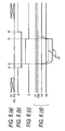
- Fig. 2 is a timing chart showing variations of the control signals for the respective FETs T2-T5 which are output from the control circuit 3, the control signal B which is input to the one input terminal of the AND circuit AND1, and various voltages.
- Fig. 2(a) shows the control signals A1-A3
- Fig. 2(b) shows the control signal B
- Fig. 2(c) shows the control signal C.
- Fig. 2(d) shows variations of the voltage V1, a voltage V2a (described later), the voltage V2, the voltage V4, and a voltage V4a (described later).
- a diagnosis is performed when all of the control signals A1-A3 are off (i.e., at the L level) and the judgment voltage is in the standard state.
- the level of the control signal B shown in Fig. 2(b) is switched from “H” to "L” at time t1, whereby the level of the signal that is supplied to the one input terminal of the AND circuit AND1 (a prohibiting unit) is made “L.” Therefore, the level of the output signal of the AND circuit AND1 is fixed to “L.” That is, output of an overcurrent judgment signal is prohibited even if it is generated by the comparator CMP1.
- the level of the control signal C shown in Fig. 2(c) is switched from “H” to "L” at time t2, whereby the FET T5 is turned off and the resistor R21 is interrupted.
- the voltage V4 comes to be generated by the series circuit of the resistors R1 and R2. Since switching is made from the combined resistance (150 k ⁇ ) of the resistors R2 and R21 (parallel connection) to the resistor R2 (600 k ⁇ ), the judgment voltage (V1 - V4) decreases rapidly (to a diagnosis judgment value). That is, the voltage V4 increases rapidly as shown in Fig. 2(d). The voltage V4 exceeds the voltage V2, whereby the output signal of the comparator CMP1 is inverted. This does not result in detection of an overcurrent because the AND circuit AND1 is prohibited from outputting an overcurrent judgment signal. Therefore, occurrence of an overcurrent is not detected.
- the control circuit 3 detects whether or not the output signal of the comparator CMP1 has been inverted. If detecting inversion, the control circuit 3 judges that the overcurrent detection circuit including the FETs T2-T4 is operating normally.
- the level of the control signal C is returned from “L” to “H” at time t3, whereupon the voltage V4 becomes lower than the voltage V2 (the judgment voltage changes from the diagnosis judgment value to the ordinary judgment value).
- the level of the control signal B is returned from "L” to "H” at time t4, whereby the ordinary overcurrent detecting function is restored.
- the above-described diagnostic function is performed at prescribed intervals by performing the above manipulations of time t1 to t4 cyclically.
- the voltage V4 becomes lower than the value in an ordinary operation (i.e., the value obtained when the resistors R2 and R21 are connected to each other in parallel). That is, as shown in Fig. 2(d), the voltage V4a which is a voltage V4 in this situation is lower, by a voltage Vx, than the value that is obtained when only the resistor R2 is effective. Therefore, the voltage V4a does not exceed the voltage V2 and the output signal of the comparator CMP1 is not inverted.
- the control circuit 3 can judge that the overcurrent detection circuit is not functional. If the control circuit 3 detects, plural times (e.g., three times) consecutively, that the output signal of the comparator CMP1 is not inverted in the processing of time t1 to t4 which is performed cyclically, the control circuit 3 judges that the overcurrent detection circuit is certainly dysfunctional. To prevent such trouble as may cause a vehicle fire in the worst case, the control circuit 3 outputs a stop signal to the driver 2 and thereby cuts off the FET T1. Furthermore, the control circuit 3 announces the occurrence of an abnormality in the overcurrent detecting function using a lamp, a buzzer, or the like (not shown).
- the resistor R102 for voltage division in an ordinary state (see Fig. 7) is replaced by the parallel connection of the resistors R2 and R21 as shown in Fig. 1 and their combined resistance is set the same as the resistance of the resistor R102 (150 k ⁇ ).
- the FET T5 is turned off, whereby the judgment voltage (V1 - V4) is made the diagnosis judgment value which is smaller than the ordinary judgment value and the output signal of the comparator CMP1 is inverted.
- the above circuit can also detect a state that the current flowing through the load 1 is unduly small. This will be described below.
- the current flowing through the load 1 i.e., load current ID
- the voltage VDS becomes low according to Equation (1). That is, the source voltage V2 of the FET T1 (i.e., the voltage V2a shown in Fig. 2(d)) becomes higher than in an ordinary state.
- the voltage V4 does not exceed the voltage V2a even if the FET T5 is turned off to increase the voltage V4.
- the control circuit 3 judges that the overcurrent detecting function is lost. This indicates that an abnormality that the current flowing through the load 1 is unduly small can also be detected by making the judgment voltage (V1 - V4) lower than in the standard state by turning off the FET T5.
- ⁇ V4 represent an increase of the voltage V4 that occurs when the FET T5 is turned off.
- V1 - V4 the relationship (V1 - V4) ⁇ VDS is established if the voltage V4 is increased by ⁇ V4 in a state that the judgment voltage (V1 - V4) is in the standard state (i.e., a control is made so that the FETs T2-T4 are turned off) assures that the overcurrent detecting function works surely when the voltage VDS is increased by ⁇ V4 or more by a line failure or the like.
- an on-failure in one or some of the FETs T2-T4 is a factor of impairing the overcurrent protecting function.
- a confirmation that the output signal of the comparator CMP1 is inverted if the voltage V4 is increased by ⁇ V4 means a confirmation that not only are the FETs T2-T4 normal but also all of the components and lines involved in the overcurrent detecting function operate normally.
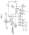
- Fig. 3 is a circuit diagram showing the configuration of a load driving device according to the second embodiment.
- the circuit according to this embodiment is the same in configuration as the circuit of Fig. 1 except that the former is equipped with resistors R6 and R7 and an FET T6.
- the resistor R6 is provided between the source of the FET T1 and the minus-side input terminal of the comparator CMP1 and a series circuit of the resistor R7 and the FET T6 is provided between one end of the resistor R6 and the ground.
- the gate of the FET T6 is connected to the source of the FET T5.
- the load driving device In an ordinary state, the load driving device according to the second embodiment operates in the same manner as that according to the first embodiment. A diagnostic operation will be described below with reference to a timing chart of Fig. 4.
- the level of the control signal B is changed to "L" at time t1, whereby the level of the output signal of the AND circuit AND1 is fixed to “L.”
- a control signal C is input to the gate of the FET T5 at time t2, whereby the FET T5 is turned off.
- the voltage V4 increases as in the case of the first embodiment.
- the voltage V4 increases in a period from time t2 to t3 and exceeds the voltage V2. Therefore, the output signal of the comparator CMP1 is inverted, and it is detected that the overcurrent protecting function is normal including the fact that no on-failure has occurred in the FETs T2-T4.
- the FET T6 is turned on at time t2, whereon a current flows through the resistors R6 and R7 and a voltage drop occurs across the resistor R6.
- a voltage V3 which is lower than the voltage V2 is supplied to the minus input terminal of the comparator CMP1. That is, the voltage (V1 - V3) is an added voltage obtained by adding a prescribed voltage to the voltage VDS (inter-electrode voltage).
- the load current ID being unduly small is detected through non-inversion of the output signal of the comparator CMP1.
- such an event can be excluded from subjects of detection because the output signal of the comparator CMP1 is inverted when the load current ID is unduly small. It is possible to consider that the FET T1 need not be cut off even in the event of an unduly small load current because, in contrast to an overcurrent, an unduly small current is not a safety-related problem.
- the second embodiment is applicable to such a case.
- Fig. 5 is a circuit diagram showing a load driving device according to the third embodiment.
- the circuit of this embodiment is different from the circuit of Fig. 3 in that the resistor R21, the FET T5 are removed and the resistor R2 (600 k ⁇ ) is replaced by a resistor R20 (150 k ⁇ ), and that a control signal C is supplied to the gate of the FET T6.
- the control signal C of this embodiment is an inverted version of the control signal shown in Fig. 4(c).
- the resistance values of the resistors R6 and R7 are changed.
- the voltage V4 is not changed and only a manipulation of adding a voltage to the voltage VDS is performed. That is, unlike in the first embodiment, the judgment voltage (V1 - V4) is not changed to the diagnosis judgment value which is smaller than the ordinary judgment value and only the processing of obtaining an added voltage by adding a prescribed voltage to the voltage VDS is performed.
- a diagnostic operation is performed in a state that the control signals A1-A3 are at the L level and that in the period from time t1 to t4 the control signal B is set to the L level to fix the output level of the AND circuit AND1 to "L.”
- the level of the control signal C is changed from “L” to "H” at time t2, whereby the FET T6 is turned on, whereupon a current flows through the resistor R6 and a voltage drop occurs there.
- the resistance values of the resistors R6 and R7 are set so that the magnitude of the voltage drop (V2 - V3) is somewhat larger than the standard judgment voltage (V1 - V4).
- load driving devices having a self-diagnosing function have been described above in the form of illustrated embodiments. However, the invention is not limited to those embodiments. Each individual part can be replaced by a desired circuit having the same function.
- a diagnosis as to whether or not an overcurrent protecting function incorporated in a semiconductor switch is performed at prescribed intervals while the semiconductor switch is conductive.
- the semiconductor switch is cut off, whereby an accident such as heat generation or a fire due to a failure in the semiconductor switch can be prevented reliably.
- the reliability of the semiconductor switch is made equivalent to a conventional switching mechanism consisting of a fuse and a relay.
- the overcurrent protecting function and the switching function can thus be implemented by a semiconductor switch.
Landscapes
- Engineering & Computer Science (AREA)
- Power Engineering (AREA)
- Electronic Switches (AREA)
- Emergency Protection Circuit Devices (AREA)
- Power Conversion In General (AREA)
Applications Claiming Priority (1)
| Application Number | Priority Date | Filing Date | Title |
|---|---|---|---|
| JP2005323439A JP4643419B2 (ja) | 2005-11-08 | 2005-11-08 | 自己診断機能を備えた負荷駆動装置 |
Publications (2)
| Publication Number | Publication Date |
|---|---|
| EP1783886A2 true EP1783886A2 (de) | 2007-05-09 |
| EP1783886A3 EP1783886A3 (de) | 2010-09-15 |
Family
ID=37835982
Family Applications (1)
| Application Number | Title | Priority Date | Filing Date |
|---|---|---|---|
| EP06023146A Withdrawn EP1783886A3 (de) | 2005-11-08 | 2006-11-07 | Lasttreibervorrichtung |
Country Status (5)
| Country | Link |
|---|---|
| US (1) | US7457089B2 (de) |
| EP (1) | EP1783886A3 (de) |
| JP (1) | JP4643419B2 (de) |
| KR (1) | KR100843366B1 (de) |
| CN (1) | CN1964191A (de) |
Cited By (4)
| Publication number | Priority date | Publication date | Assignee | Title |
|---|---|---|---|---|
| EP2040364A3 (de) * | 2007-09-20 | 2012-08-08 | Hitachi Ltd. | Lastantriebsschaltung |
| EP2432112A4 (de) * | 2009-05-27 | 2014-10-22 | Sanden Corp | Motorsteuervorrichtung |
| EP2949516A4 (de) * | 2013-01-23 | 2016-10-19 | Yazaki Corp | Stromversorgungsregler für fahrzeuge |
| EP3361588A1 (de) * | 2017-02-09 | 2018-08-15 | Ellenberger & Poensgen GmbH | Verfahren zum betreiben eines elektronischen schutzschalters und elektronischer schutzschalter |
Families Citing this family (41)
| Publication number | Priority date | Publication date | Assignee | Title |
|---|---|---|---|---|
| JP4570173B2 (ja) * | 2006-06-01 | 2010-10-27 | 株式会社オートネットワーク技術研究所 | 電力供給制御装置 |
| US7843248B1 (en) * | 2007-11-01 | 2010-11-30 | Intersil Americas Inc. | Analog switch with overcurrent detection |
| JP5044448B2 (ja) | 2008-03-03 | 2012-10-10 | ルネサスエレクトロニクス株式会社 | 電源スイッチ回路 |
| JP5171406B2 (ja) * | 2008-06-05 | 2013-03-27 | 矢崎総業株式会社 | 負荷回路の過電流保護装置 |
| US8232742B2 (en) | 2008-11-27 | 2012-07-31 | Arkalumen Inc. | Method, apparatus and computer-readable media for controlling lighting devices |
| JP2010158109A (ja) | 2008-12-26 | 2010-07-15 | Yazaki Corp | 負荷回路の保護装置 |
| JP5702570B2 (ja) * | 2009-11-27 | 2015-04-15 | ローム株式会社 | オペアンプ及びこれを用いた液晶駆動装置、並びに、パラメータ設定回路、半導体装置、電源装置 |
| US8564214B2 (en) * | 2010-05-11 | 2013-10-22 | Arkalumen Inc. | Circuits for sensing current levels within lighting apparatus |
| US9086435B2 (en) | 2011-05-10 | 2015-07-21 | Arkalumen Inc. | Circuits for sensing current levels within a lighting apparatus incorporating a voltage converter |
| US9089024B2 (en) | 2010-05-11 | 2015-07-21 | Arkalumen Inc. | Methods and apparatus for changing a DC supply voltage applied to a lighting circuit |
| JP5530306B2 (ja) * | 2010-08-25 | 2014-06-25 | 矢崎総業株式会社 | 過電流検出装置 |
| JP5146786B2 (ja) * | 2010-09-24 | 2013-02-20 | 株式会社デンソー | 電子装置 |
| JP2012125377A (ja) * | 2010-12-15 | 2012-07-05 | Sammy Corp | 遊技機 |
| US9192009B2 (en) | 2011-02-14 | 2015-11-17 | Arkalumen Inc. | Lighting apparatus and method for detecting reflected light from local objects |
| CA2867678C (en) | 2011-03-16 | 2016-06-14 | Arkalumen Inc. | Lighting apparatus and methods for controlling lighting apparatus using ambient light levels |
| US8939604B2 (en) | 2011-03-25 | 2015-01-27 | Arkalumen Inc. | Modular LED strip lighting apparatus |
| US9060400B2 (en) | 2011-07-12 | 2015-06-16 | Arkalumen Inc. | Control apparatus incorporating a voltage converter for controlling lighting apparatus |
| CN104272594B (zh) * | 2012-05-01 | 2018-04-27 | 大岛俊蔵 | 过电流保护电源装置 |
| JP5860362B2 (ja) * | 2012-08-22 | 2016-02-16 | 日本特殊陶業株式会社 | 負荷駆動装置 |
| JP6267232B2 (ja) * | 2013-11-29 | 2018-01-24 | 日立オートモティブシステムズ株式会社 | 負荷駆動回路 |
| JP6230397B2 (ja) | 2013-12-11 | 2017-11-15 | 新電元工業株式会社 | 故障検知装置およびそのプログラム |
| JP6400610B2 (ja) * | 2014-02-06 | 2018-10-03 | 日立オートモティブシステムズ株式会社 | 負荷駆動回路 |
| JP6311357B2 (ja) * | 2014-03-05 | 2018-04-18 | 株式会社オートネットワーク技術研究所 | 防止装置 |
| JP6260552B2 (ja) * | 2015-02-26 | 2018-01-17 | 株式会社オートネットワーク技術研究所 | 電力供給装置 |
| US9992836B2 (en) | 2015-05-05 | 2018-06-05 | Arkawmen Inc. | Method, system and apparatus for activating a lighting module using a buffer load module |
| US9775211B2 (en) | 2015-05-05 | 2017-09-26 | Arkalumen Inc. | Circuit and apparatus for controlling a constant current DC driver output |
| US10225904B2 (en) | 2015-05-05 | 2019-03-05 | Arkalumen, Inc. | Method and apparatus for controlling a lighting module based on a constant current level from a power source |
| US10568180B2 (en) | 2015-05-05 | 2020-02-18 | Arkalumen Inc. | Method and apparatus for controlling a lighting module having a plurality of LED groups |
| US9992829B2 (en) | 2015-05-05 | 2018-06-05 | Arkalumen Inc. | Control apparatus and system for coupling a lighting module to a constant current DC driver |
| JP6506644B2 (ja) * | 2015-07-09 | 2019-04-24 | 日立オートモティブシステムズ株式会社 | 駆動装置 |
| WO2017134824A1 (ja) | 2016-02-05 | 2017-08-10 | 俊蔵 大島 | 電源装置 |
| JP6610446B2 (ja) * | 2016-06-21 | 2019-11-27 | 株式会社オートネットワーク技術研究所 | 給電制御装置 |
| JP6575458B2 (ja) * | 2016-08-10 | 2019-09-18 | 株式会社デンソー | 異常診断装置 |
| US10910815B2 (en) * | 2017-04-25 | 2021-02-02 | Hitachi Automotive Systems, Ltd. | Electronic control unit |
| TWI666674B (zh) * | 2018-07-12 | 2019-07-21 | 康舒科技股份有限公司 | 具有電子斷路器的電源供應設備及其控制方法 |
| JP7254827B2 (ja) * | 2018-09-21 | 2023-04-10 | 日立Astemo株式会社 | 電子制御装置 |
| EP3629039B1 (de) * | 2018-09-26 | 2023-04-05 | Aptiv Technologies Limited | Halbleiter-leistungsschaltervorrichtung |
| JP7140045B2 (ja) * | 2019-05-15 | 2022-09-21 | 株式会社デンソー | 駆動回路 |
| CN113125931B (zh) * | 2019-12-30 | 2024-03-26 | 日立安斯泰莫汽车系统(苏州)有限公司 | 电路异常诊断装置、电路异常诊断方法及计算机可读取介质 |
| CN115378412A (zh) * | 2021-05-20 | 2022-11-22 | 长鑫存储技术有限公司 | 比较电路及存储器 |
| JP2025086241A (ja) * | 2023-11-27 | 2025-06-06 | 株式会社オートネットワーク技術研究所 | 車載装置 |
Citations (2)
| Publication number | Priority date | Publication date | Assignee | Title |
|---|---|---|---|---|
| US6504697B1 (en) | 1997-02-10 | 2003-01-07 | Daimlerchrysler Ag | Arrangement and method for measuring a temperature |
| US20050237689A1 (en) | 2004-04-26 | 2005-10-27 | Siemens Aktiengesellschaft | Method and device for protecting an electronic component |
Family Cites Families (11)
| Publication number | Priority date | Publication date | Assignee | Title |
|---|---|---|---|---|
| JPS6041321A (ja) * | 1983-08-16 | 1985-03-05 | Fujikura Ltd | 入力回路 |
| JPH0954493A (ja) * | 1995-08-11 | 1997-02-25 | Ricoh Co Ltd | 現像装置 |
| JP3424489B2 (ja) * | 1997-03-24 | 2003-07-07 | 日産自動車株式会社 | 半導体過電流検知回路とその検査方法 |
| US6934139B2 (en) * | 2000-05-01 | 2005-08-23 | Fuji Electric Device Technology Co., Ltd. | Intelligent power module |
| JP3914004B2 (ja) * | 2001-05-25 | 2007-05-16 | 矢崎総業株式会社 | 半導体素子の過電流検出・保護装置 |
| US7149065B2 (en) * | 2003-06-16 | 2006-12-12 | Hubbell Incorporated | Self testing digital fault interrupter |
| US7128385B2 (en) * | 2004-06-30 | 2006-10-31 | Lexmark International, Inc. | System and method for ink jet printhead detection |
| JP4504222B2 (ja) * | 2005-02-21 | 2010-07-14 | 矢崎総業株式会社 | 過電流検出装置 |
| US7382595B2 (en) * | 2005-05-25 | 2008-06-03 | Electronic Theatre Controls, Inc. | Low voltage overcurrent protection for solid state switching system |
| JP4713963B2 (ja) * | 2005-07-07 | 2011-06-29 | 矢崎総業株式会社 | 過電流検出装置 |
| JP2007095001A (ja) * | 2005-09-30 | 2007-04-12 | Noritsu Koki Co Ltd | プリント処理システム |
-
2005
- 2005-11-08 JP JP2005323439A patent/JP4643419B2/ja not_active Expired - Fee Related
-
2006
- 2006-11-02 KR KR1020060107868A patent/KR100843366B1/ko not_active Expired - Fee Related
- 2006-11-06 US US11/593,020 patent/US7457089B2/en not_active Expired - Fee Related
- 2006-11-07 CN CNA2006101439435A patent/CN1964191A/zh active Pending
- 2006-11-07 EP EP06023146A patent/EP1783886A3/de not_active Withdrawn
Patent Citations (2)
| Publication number | Priority date | Publication date | Assignee | Title |
|---|---|---|---|---|
| US6504697B1 (en) | 1997-02-10 | 2003-01-07 | Daimlerchrysler Ag | Arrangement and method for measuring a temperature |
| US20050237689A1 (en) | 2004-04-26 | 2005-10-27 | Siemens Aktiengesellschaft | Method and device for protecting an electronic component |
Cited By (7)
| Publication number | Priority date | Publication date | Assignee | Title |
|---|---|---|---|---|
| EP2040364A3 (de) * | 2007-09-20 | 2012-08-08 | Hitachi Ltd. | Lastantriebsschaltung |
| US8548641B2 (en) | 2007-09-20 | 2013-10-01 | Hitachi, Ltd. | Load drive circuit |
| EP2432112A4 (de) * | 2009-05-27 | 2014-10-22 | Sanden Corp | Motorsteuervorrichtung |
| EP2949516A4 (de) * | 2013-01-23 | 2016-10-19 | Yazaki Corp | Stromversorgungsregler für fahrzeuge |
| US9932001B2 (en) | 2013-01-23 | 2018-04-03 | Yazaki Corporation | Vehicular power source controller |
| EP3361588A1 (de) * | 2017-02-09 | 2018-08-15 | Ellenberger & Poensgen GmbH | Verfahren zum betreiben eines elektronischen schutzschalters und elektronischer schutzschalter |
| US10777997B2 (en) | 2017-02-09 | 2020-09-15 | Ellenberger & Poensgen Gmbh | Method for operating an electronic circuit breaker, and electronic circuit breaker |
Also Published As
| Publication number | Publication date |
|---|---|
| US20070103832A1 (en) | 2007-05-10 |
| KR20070049561A (ko) | 2007-05-11 |
| EP1783886A3 (de) | 2010-09-15 |
| CN1964191A (zh) | 2007-05-16 |
| JP4643419B2 (ja) | 2011-03-02 |
| KR100843366B1 (ko) | 2008-07-02 |
| JP2007134780A (ja) | 2007-05-31 |
| US7457089B2 (en) | 2008-11-25 |
Similar Documents
| Publication | Publication Date | Title |
|---|---|---|
| EP1783886A2 (de) | Lasttreibervorrichtung | |
| CN109791175B (zh) | 半桥驱动器故障诊断系统和方法 | |
| JP4943939B2 (ja) | 過電流保護装置 | |
| JP5451563B2 (ja) | モータ制御装置 | |
| DE112016000948T5 (de) | Stromversorgungsvorrichtung | |
| JP4158754B2 (ja) | 過電流検知方法および検知回路 | |
| CN114079262A (zh) | 触发电路和包括该触发电路的电子保险丝装置 | |
| EP1770863B1 (de) | Überstromschutzvorrichtung | |
| US20090033268A1 (en) | Power supply system with function of short circuit detection | |
| EP2040364A2 (de) | Lastantriebsschaltung | |
| JPWO2018016225A1 (ja) | 車載制御装置 | |
| US10882475B2 (en) | Multi-voltage control device for a motor vehicle, motor vehicle and operating method for the control device | |
| JP2008276727A (ja) | 負荷駆動装置 | |
| JP7651900B2 (ja) | 異常検出装置、及び異常検出方法 | |
| KR102098049B1 (ko) | 과전류 발생시 모터 구동 전원을 차단하는 eps 제어 장치 및 방법 | |
| EP2293442A1 (de) | Überstromschutzeinrichtung für eine lastschaltung | |
| JPH10278730A (ja) | 乗員保護装置の故障診断装置 | |
| CN109690333B (zh) | 电子控制装置和电子控制装置的连接状态的诊断方法 | |
| WO2022244687A1 (ja) | 遮断制御装置、及び遮断制御システム | |
| CN101341641A (zh) | 具有故障监测的电机控制电路 | |
| US11982247B2 (en) | Load drive device | |
| US11507042B2 (en) | High current and power limiting circuit for I/O modules with internal output power support | |
| EP4510403A1 (de) | Redundante stromversorgung | |
| JPH06225443A (ja) | 給電制御装置 | |
| JP3152000B2 (ja) | パワートランジスタ保護回路 |
Legal Events
| Date | Code | Title | Description |
|---|---|---|---|
| PUAI | Public reference made under article 153(3) epc to a published international application that has entered the european phase |
Free format text: ORIGINAL CODE: 0009012 |
|
| 17P | Request for examination filed |
Effective date: 20061107 |
|
| AK | Designated contracting states |
Kind code of ref document: A2 Designated state(s): AT BE BG CH CY CZ DE DK EE ES FI FR GB GR HU IE IS IT LI LT LU LV MC NL PL PT RO SE SI SK TR |
|
| AX | Request for extension of the european patent |
Extension state: AL BA HR MK YU |
|
| RAP1 | Party data changed (applicant data changed or rights of an application transferred) |
Owner name: YAZAKI CORPORATION |
|
| PUAL | Search report despatched |
Free format text: ORIGINAL CODE: 0009013 |
|
| AK | Designated contracting states |
Kind code of ref document: A3 Designated state(s): AT BE BG CH CY CZ DE DK EE ES FI FR GB GR HU IE IS IT LI LT LU LV MC NL PL PT RO SE SI SK TR |
|
| AX | Request for extension of the european patent |
Extension state: AL BA HR MK RS |
|
| AKX | Designation fees paid |
Designated state(s): DE FR GB IT |
|
| 17Q | First examination report despatched |
Effective date: 20160114 |
|
| STAA | Information on the status of an ep patent application or granted ep patent |
Free format text: STATUS: THE APPLICATION IS DEEMED TO BE WITHDRAWN |
|
| 18D | Application deemed to be withdrawn |
Effective date: 20160525 |