EP1906453B1 - Dispositif semi-conducteur de puissance - Google Patents
Dispositif semi-conducteur de puissance Download PDFInfo
- Publication number
- EP1906453B1 EP1906453B1 EP07008113.8A EP07008113A EP1906453B1 EP 1906453 B1 EP1906453 B1 EP 1906453B1 EP 07008113 A EP07008113 A EP 07008113A EP 1906453 B1 EP1906453 B1 EP 1906453B1
- Authority
- EP
- European Patent Office
- Prior art keywords
- gate
- polysilicon film
- doped
- impurities
- semiconductor layer
- Prior art date
- Legal status (The legal status is an assumption and is not a legal conclusion. Google has not performed a legal analysis and makes no representation as to the accuracy of the status listed.)
- Ceased
Links
Images


Classifications
-
- H—ELECTRICITY
- H10—SEMICONDUCTOR DEVICES; ELECTRIC SOLID-STATE DEVICES NOT OTHERWISE PROVIDED FOR
- H10D—INORGANIC ELECTRIC SEMICONDUCTOR DEVICES
- H10D12/00—Bipolar devices controlled by the field effect, e.g. insulated-gate bipolar transistors [IGBT]
- H10D12/411—Insulated-gate bipolar transistors [IGBT]
- H10D12/441—Vertical IGBTs
-
- H—ELECTRICITY
- H10—SEMICONDUCTOR DEVICES; ELECTRIC SOLID-STATE DEVICES NOT OTHERWISE PROVIDED FOR
- H10D—INORGANIC ELECTRIC SEMICONDUCTOR DEVICES
- H10D12/00—Bipolar devices controlled by the field effect, e.g. insulated-gate bipolar transistors [IGBT]
- H10D12/411—Insulated-gate bipolar transistors [IGBT]
- H10D12/441—Vertical IGBTs
- H10D12/461—Vertical IGBTs having non-planar surfaces, e.g. having trenches, recesses or pillars in the surfaces of the emitter, base or collector regions
- H10D12/481—Vertical IGBTs having non-planar surfaces, e.g. having trenches, recesses or pillars in the surfaces of the emitter, base or collector regions having gate structures on slanted surfaces, on vertical surfaces, or in grooves, e.g. trench gate IGBTs
-
- H—ELECTRICITY
- H10—SEMICONDUCTOR DEVICES; ELECTRIC SOLID-STATE DEVICES NOT OTHERWISE PROVIDED FOR
- H10D—INORGANIC ELECTRIC SEMICONDUCTOR DEVICES
- H10D62/00—Semiconductor bodies, or regions thereof, of devices having potential barriers
- H10D62/10—Shapes, relative sizes or dispositions of the regions of the semiconductor bodies; Shapes of the semiconductor bodies
- H10D62/124—Shapes, relative sizes or dispositions of the regions of semiconductor bodies or of junctions between the regions
- H10D62/126—Top-view geometrical layouts of the regions or the junctions
- H10D62/127—Top-view geometrical layouts of the regions or the junctions of cellular field-effect devices, e.g. multicellular DMOS transistors or IGBTs
-
- H—ELECTRICITY
- H10—SEMICONDUCTOR DEVICES; ELECTRIC SOLID-STATE DEVICES NOT OTHERWISE PROVIDED FOR
- H10D—INORGANIC ELECTRIC SEMICONDUCTOR DEVICES
- H10D62/00—Semiconductor bodies, or regions thereof, of devices having potential barriers
- H10D62/10—Shapes, relative sizes or dispositions of the regions of the semiconductor bodies; Shapes of the semiconductor bodies
- H10D62/13—Semiconductor regions connected to electrodes carrying current to be rectified, amplified or switched, e.g. source or drain regions
- H10D62/149—Source or drain regions of field-effect devices
- H10D62/151—Source or drain regions of field-effect devices of IGFETs
-
- H—ELECTRICITY
- H10—SEMICONDUCTOR DEVICES; ELECTRIC SOLID-STATE DEVICES NOT OTHERWISE PROVIDED FOR
- H10D—INORGANIC ELECTRIC SEMICONDUCTOR DEVICES
- H10D64/00—Electrodes of devices having potential barriers
- H10D64/111—Field plates
- H10D64/117—Recessed field plates, e.g. trench field plates or buried field plates
-
- H—ELECTRICITY
- H10—SEMICONDUCTOR DEVICES; ELECTRIC SOLID-STATE DEVICES NOT OTHERWISE PROVIDED FOR
- H10D—INORGANIC ELECTRIC SEMICONDUCTOR DEVICES
- H10D64/00—Electrodes of devices having potential barriers
- H10D64/20—Electrodes characterised by their shapes, relative sizes or dispositions
- H10D64/27—Electrodes not carrying the current to be rectified, amplified, oscillated or switched, e.g. gates
- H10D64/311—Gate electrodes for field-effect devices
- H10D64/411—Gate electrodes for field-effect devices for FETs
- H10D64/511—Gate electrodes for field-effect devices for FETs for IGFETs
- H10D64/512—Disposition of the gate electrodes, e.g. buried gates
- H10D64/513—Disposition of the gate electrodes, e.g. buried gates within recesses in the substrate, e.g. trench gates, groove gates or buried gates
-
- H—ELECTRICITY
- H10—SEMICONDUCTOR DEVICES; ELECTRIC SOLID-STATE DEVICES NOT OTHERWISE PROVIDED FOR
- H10D—INORGANIC ELECTRIC SEMICONDUCTOR DEVICES
- H10D64/00—Electrodes of devices having potential barriers
- H10D64/20—Electrodes characterised by their shapes, relative sizes or dispositions
- H10D64/27—Electrodes not carrying the current to be rectified, amplified, oscillated or switched, e.g. gates
- H10D64/311—Gate electrodes for field-effect devices
- H10D64/411—Gate electrodes for field-effect devices for FETs
- H10D64/511—Gate electrodes for field-effect devices for FETs for IGFETs
- H10D64/514—Gate electrodes for field-effect devices for FETs for IGFETs characterised by the insulating layers
- H10D64/516—Gate electrodes for field-effect devices for FETs for IGFETs characterised by the insulating layers the thicknesses being non-uniform
-
- H—ELECTRICITY
- H10—SEMICONDUCTOR DEVICES; ELECTRIC SOLID-STATE DEVICES NOT OTHERWISE PROVIDED FOR
- H10D—INORGANIC ELECTRIC SEMICONDUCTOR DEVICES
- H10D64/00—Electrodes of devices having potential barriers
- H10D64/60—Electrodes characterised by their materials
- H10D64/66—Electrodes having a conductor capacitively coupled to a semiconductor by an insulator, e.g. MIS electrodes
- H10D64/661—Electrodes having a conductor capacitively coupled to a semiconductor by an insulator, e.g. MIS electrodes the conductor comprising a layer of silicon contacting the insulator, e.g. polysilicon having vertical doping variation
Definitions
- the present invention relates to power semiconductor devices having a MOS-gate-metal-oxide semiconductor gate-structure, especially to an insulated gate bipolar transistor used in devices such as invertors that transform or control electric power.
- US 6 451 644 B1 discloses an ultra-large scale integrated (ULSI) circuit including MOSFETs having a gate conductor with dopants distributed in a box-like distribution. The dopants also achieve high electrical activation.
- the MOSFETs utilize gate structures with heavily doped polysilicon material or heavily doped polysilicon and germanium material.
- GB 2 306 249 A describes a termination structure for semiconductor devices and a process for fabricating the termination structure.
- the termination structure includes a polysilicon field plate located atop a portion of a field oxide region and overlaying a portion of the base region.
- US 6 218 217 B1 discloses IGBTs with one or more emitter trenches between two gate trenches.
- JP 2001 168333 A aims at increasing the discharge resistance of holes in an IGBT structure without narrowing the distance between trenches.
- a so-called restriction trench in contact with the emitter electrode is formed in such a way that it passes through the base layer so as to reach the drift layer between a pair of emitter layers.
- the restriction trench increases the discharge resistance of the holes when the discharge route of the holes from the drift region through the base layer to an emitter electrode is narrow.
- WO 02/27800 A2 describes a trench DMOS transistor having lightly doped source structure.
- a gate trench polysilicon is deposited in a two-step process. In the first step, a layer of undoped polysilicon is deposited to line the sidewalls of the trenches. The undoped polysilicon layer then is followed by the deposition of a layer of doped polysilicon.
- US 2003/0057478 A1 describes a MOS-gated power semiconductor device.
- the device includes a semiconductor substrate that is heavily doped with impurities and used as a collector region, a lightly doped drift region, a gate insulating layer on the drift region having a center thicker than its edges, a gate electrode on the gate insulating layer and a well region that is lightly doped and located on the drift region and has a channel region overlapping a portion of the gate electrode.
- IGBTs insulated gate bipolar transistors
- IGBTs insulated gate bipolar transistors
- IGBTs are utilized, in many cases, as power semiconductor devices including invertors that transform or control electric power.
- IGBTs are required to obtain larger current capacity (higher withstand voltage) and higher reliability.
- Fig. 4 is a plane view of an IGBT-chip that is illustrated in Patent Document 1, for example.
- a numeral '51' represents an emitter electrode (a first main electrode); '52', a gate pad formed at a concave portion that is provided on a peripheral portion of the emitter electrode 51; '53', gate wiring that extends from the gate pad 52 and is provided on peripheral surface of the emitter electrode 51 and on the inner surface thereof so as to divide the emitter electrode 51 into strips.
- IGBT cells 54 having a cellular structure are formed in spaces divided by the gate wire 53.
- Fig. 5 is a partially sectional view along Line A-A of one of the IGBT cells 54 in Fig. 4 , and shows a cellar structure of a general planar-gate-type IGBT illustrated in Non-Patent Document 1.
- Fig. 5 is a partially sectional view along Line A-A of one of the IGBT cells 54 in Fig. 4 , and shows a cellar structure of a general planar-gate-type IGBT illustrated in Non-Patent Document 1.
- Fig. 5 is a partially sectional view along Line A-A of one of the IGBT cells 54 in Fig. 4 , and shows a cellar structure of a general planar-gate-type IGBT illustrated in Non-Patent Document 1.
- a numeral '55' represents a p + collector layer (a first semiconductor layer of a first conductivity type) made of a semiconductor substrate; '56', an n + buffer layer (a second semiconductor layer of a second conductivity type) provided on the top side of the p + collector layer 55; '57', an n- layer (a third semiconductor layer of the second conductivity type) provided on the n + buffer layer 56; '58', a p base region (a first semiconductor region of the first conductivity type) provided selectively in the top side of the n - layer 57; '59', an n + emitter region (a second semiconductor region of the second conductivity type) provided selectively in the top side of the p base region 58; '60', a gate insulation film that is made of a dielectric material such as an oxide film and is provided on the n - layer 57, partially on the n + emitter region 59 and on the p base region 58 therebetween; '61',
- a numeral '63' represents a collector electrode (a second main electrode) that is provided on the bottom surface of the p + collector layer 55 and is made of a conductive material such as aluminum.
- the gate electrode 61 is connected to the gate wiring 53 at the electrode ends provided in its extension orientation (in the front-back orientation with respect to the document face in Fig. 5 ).
- Fig. 6 is a partially sectional view along Line A-A of the one of IGBT cells 54 in Fig. 4 ; the figure shows a cellular structure of a planar-gate-type IGBT that has a terrace gate structure shown in Patent Document 2.
- a terrace gate portion 65 is provided on the n - layer 57 in Fig. 6 , which differs from Fig. 5 ; whose feature is that the IGBT has a thicker gate insulation film 60 than that of the average planar-gate-type IGBT.
- the capacity of the gate insulation film becomes smaller, reducing its feedback capacity.
- the portions that are identical or equivalent to those in Fig. 5 are represented by the same numerals as those in Fig. 5 so as to omit their explanations.
- IGBT that is a conventional power semiconductor device has been configured as described above; recently, it is required that IGBTs obtain larger current capacity (higher withstand voltage) and higher reliability; the following problems have now drawn attention in order to meet those requirements.
- the gate wiring 53 formed of a conductive material such as aluminum is provided as shown in Fig. 4 , so as to divide the emitter electrode 51 into strips.
- the number of wires that are made of a conductive material such as aluminum and bonded to the emitter electrode 51 tends to increase in an IGBT package where the IGBT chip 50 is mounted.
- a current supplied to one of the IGBT cells 54 close to the gate wiring 53 and a current supplied to another one of the IGBT cells 54 apart from the gate wiring are not balanced (hereinafter, referred as imbalance among current diversions); then, currents are concentrated on such IGBT cells 54 that are located apart from the gate wiring 53 and whose turning off speed becomes slow, so that the IGBT cells generate heat; therefore, turn-off withstand ability, that is, a reverse-biased safe operating area (hereinafter, referred as RBSOA), becomes reduced.
- RBSOA reverse-biased safe operating area
- doped polysilicon that is a polysilicon-the material of the gate electrode 61-doped with impurities in order to reduce their resistance.
- doped silicon is used for the gate electrode 61 of the planar-gate-type IGBT shown in Fig. 5 and Fig. 6 .
- auto-doping of impurities, with which a polysilicon has been doped, into the gate insulation film 60 and the n - layer 57 occurs, adversely affecting the gate-emitter leakage current and the primary-voltage-to-leakage-current characteristics. Therefore, in the above-described case where the spaces between the gate wiring 53 become wider, the gate resistances increase, causing the imbalance among current diversions to occur, so that its turn-off withstand ability will be reduced.
- the present invention is aimed to solve the problems above-described; an object thereof is, even when the spaces between the gate wiring 53 become wide, to provide a power semiconductor device that can meet requirements for larger current capacity and higher reliability while improving imbalance among current diversions.
- a power semiconductor device is configured so as to have a gate electrode including a polysilicon film provided on a gate insulation film, and a doped polysilicon film-a polysilicon doped with impurities to reduce its resistance-that is provided on the polysilicon film; the gate resistance of the gate electrode can be reduced in comparison to conventional ones. Therefore, the imbalance among current diversions at turn-off is improved so as not to reduce turn-off withstand ability of the device.
- a polysilicon film not doped with impurities is provided between a doped polysilicon film and a gate insulation film, it is possible to preclude auto-doping of impurities, which might be feared by providing with the doped polysilicon film, into the gate insulation film and an n- layer from adversely affecting gate-emitter leakage current and collector-emitter leakage current. Therefore, a power semiconductor device that meets requirements for increased current capacity and higher reliability can be obtained.
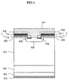
- Fig. 1 is a partial cross-sectional view illustrating a planar-gate-type IGBT that is a power semiconductor device according to Example 1; the figure illustrates, taking along the line A-A, a cross-sectional cellar structure of the IGBT cells 54 shown in Fig. 4 .
- Fig. 1 differs from Fig. 5 that represents prior art as follows; a gate electrode includes a polysilicon film 1a provided on the gate insulation film 60, and a doped polysilicon film 1b that is doped with impurities and provided on the polysilicon film 1a; the gate electrode 1 is connected to the gate wiring 53 at the electrode ends provided in its extension orientation (in the front-back orientation with respect to the document face in Fig. 1 ). Because the other components are identical or equivalent to those in Fig. 5 , the same numerals will be used so as to omit their explanations.
- the gate electrode includes the polysilicon film 1a provided on the gate insulation film 60, and the doped polysilicon film 1b that is doped with impurities to reduce its resistance and is provided on the polysilicon film 1a, the gate resistance of the gate electrode 1 can be reduced in comparison to conventional ones. Therefore, the difference between the gate resistance of a first one of the IGBT cells 54 close to the gate wiring 53 and that of a second one of the IGBT cells 54 apart from the gate wiring (for example, being located at the intermediary point between the gate wiring) becomes small.
- the IGBT cells 54 turn off, the imbalance between a current supplied to the first one of the IGBT cells 54 close to the gate wiring 53 and a current supplied to the second one of the IGBT cells 54 apart from the gate wiring 53 is improved; because currents are not concentrated at the second one of the IGBT cells 54 apart from the gate wiring 53, the IGBT cell does not generate heat, so as to prevent its turn-off withstand ability from reducing.
- the polysilicon film 1a not doped with impurities is provided between the doped polysilicon film 1b and the gate insulation film 60, the impurities contained in the doped polysilicon film 1b are prevented from naturally diffusing, namely, auto-doping into the gate insulation film 60 and the n - layer 57. Therefore, it is possible to preclude expected influence of auto-doping on gate-emitter leakage current and collector-emitter leakage current.
- Example 1 a gate electrode 1 has been explained, in which the gate electrode 1 is configured with the polysilicon film 1a provided on the gate insulation film 60, and the doped polysilicon film 1b that is doped with impurities to reduce its resistance and is provided on the polysilicon film 1a.
- One of Figs. 2 is a partially enlarged view for explaining Embodiment 1; the figure corresponds to a view in which the gate electrode 1 in Fig. 1 is partially enlarged.
- Embodiment 1 differs from Example 1 in that gradient of concentration with respect to impurities is provided in the doped polysilicon film 1b. More specifically, as distribution of its impurity concentration shown in the middle view of Figs.
- the impurity concentration is made to vary in a thickness direction of the doped polysilicon film 1b; at the top portion of the doped polysilicon 1b, the value of impurity concentration takes its maximum value; the value becomes smaller heading thickness-wise toward the polysilicon film 1a; at the bottom portion of the doped polysilicon film 1b, which is contiguous with the polysilicon, the value takes its lowest value or zero.
- the portions that are identical or equivalent to those in Fig. 5 are represented by the same numerals as those in Fig. 5 so as to omit their explanations.
- the resistance of the gate electrode 1 becomes distributed as shown in the right view of Figs. 2 ; the doped silicon film 1b has at its top area a portion in which its resistance is reduced, which prevents the turn-off withstand ability from reducing as in the case of Example 1.
- the impurities contained in the doped polysilicon film 1b are prevented much more than Example 1, from diffusing naturally, namely, auto-doping into the gate insulation film 60 and the n - layer 57. Therefore, it is possible to further preclude expected influence of auto-doping on gate-emitter leakage current and collector-emitter leakage current.
- the gate electrode 1 configured with a polysilicon film 1a and a doped polysilicon 1b that have been explained in Example 1, is also applicable to a planar-gate-type IGBT that has a terrace gate structure shown in Fig. 6 .
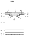
- Fig. 3 is a partial cross-sectional view illustrating a planar-gate-type IGBT that is a power semiconductor device having the terrace gate structure, according to Example 2; the figure illustrates, taking along the line A-A, a cellar structure of the IGBT cells 54 shown in Fig. 4 .
- Fig. 3 differs from Fig.
- a terrace gate portion 65 of a gate electrode 2 is configured with a polysilicon film 2a provided on a gate insulation film 60, and with the doped polysilicon film 2b that is provided on the polysilicon film 2a and is doped with impurities to reduce its resistance.
- the gate electrode 2 is connected to the gate wiring 53 at the electrode ends provided in its extension orientation (in the front-back orientation with respect to the document face in Fig. 3 ). Because the other components are identical or equivalent to those in Fig. 5 and Fig. 6 , the same numerals will be used so as to omit their explanations.
- the terrace gate portion 65 of the gate electrode 2 is configured with the polysilicon film 2a provided on the gate insulation film 60, and with the doped polysilicon film 2b that is provided on the polysilicon film 2a and is doped with impurities to reduce its resistance, the gate resistance of the gate electrode 2 can be reduced in comparison to that of conventional devices. Therefore, as is the case with
- Example 1 the turn-off withstand ability of the device can be prevented from reducing.
- the impurities contained in the doped polysilicon film 2b are prevented from diffusing naturally, namely, auto-doping into the gate insulation film 60 and the n - layer 57. Therefore, it is possible to preclude expected influence of auto-doping on gate-emitter leakage current and collector-emitter leakage current.
- Example 2 a terrace gate has been explained, as follows; the terrace gate portion 65 of the gate electrode 2 is configured with the polysilicon film 2a provided on the gate insulation film 60, and with the doped polysilicon film 2b that is provided on the polysilicon film 2a and is doped with impurities to reduce its resistance.
- the value of impurity concentration may vary in a similar fashion to that of Embodiment 1.
Landscapes
- Electrodes Of Semiconductors (AREA)
Claims (2)
- Dispositif semi-conducteur de puissance, comprenant :une première couche semi-conductrice (55) d'un premier type de conductivité ;une deuxième couche semi-conductrice (56) d'un deuxième type de conductivité, prévue sur la partie supérieure de la première couche semi-conductrice ;une troisième couche semi-conductrice (57) du deuxième type de conductivité, prévue sur la deuxième couche semi-conductrice ;une première région semi-conductrice (58) du premier type de conductivité, prévue sélectivement dans la partie supérieure de la troisième couche semi-conductrice (57) ;une deuxième région semi-conductrice (59) du deuxième type de conductivité, prévue sélectivement dans la partie supérieure de la première région semi-conductrice (58) ;un film d'isolation de grille (60) prévu sur la troisième couche semi-conductrice (57), sur la première région semi-conductrice (58) et partiellement sur la deuxième région semi-conductrice (59) ;une électrode de grille (1) comprenant un film de polysilicium (1a) prévu sur le film d'isolation de grille (60) et un film de polysilicium dopé (1b) qui est prévu sur le film de polysilicium (1a) et dopé avec des impuretés ;une première électrode principale (51) qui est prévue sur la première région semi-conductrice (58) et est reliée électriquement à la deuxième région semi-conductrice (59) ;une deuxième électrode principale (63) prévue sur la partie inférieure de la première région semi-conductrice (55) ;ledit film de polysilicium (1a) prévu sur le film d'isolation de grille (60) n'étant pas dopé avec des impuretés, dans lequel le film de polysilicium dopé (1b) a un gradient de concentration sur toute son épaisseur par rapport aux impuretés dans le sens de son épaisseur et le gradient de concentration donne la concentration la plus élevée des impuretés dans la partie supérieure du film de polysilicium dopé (1b) et donne la concentration la plus faible des impuretés dans la partie inférieure du film de polysilicium dopé (1b),dans lequel la valeur de la concentration des impuretés diminue en allant dans le sens de l'épaisseur vers le film de polysilicium (1a).
- Dispositif semi-conducteur de puissance selon la revendication 1, dans lequel le dispositif semi-conducteur de puissance comprend en outre une partie de grille en terrasse (65) qui est une partie épaissie du film d'isolation de grille prévu sur la troisième couche semi-conductrice (57) et le film de polysilicium dopé est prévu seulement sur une partie du film de polysilicium qui couvre la grille en terrasse (65).
Priority Applications (1)
| Application Number | Priority Date | Filing Date | Title |
|---|---|---|---|
| EP14150497.7A EP2731142A3 (fr) | 2006-09-29 | 2007-04-20 | Dispositif semi-conducteur de puissance |
Applications Claiming Priority (1)
| Application Number | Priority Date | Filing Date | Title |
|---|---|---|---|
| JP2006267137A JP5128100B2 (ja) | 2006-09-29 | 2006-09-29 | 電力用半導体装置 |
Related Child Applications (2)
| Application Number | Title | Priority Date | Filing Date |
|---|---|---|---|
| EP14150497.7A Division-Into EP2731142A3 (fr) | 2006-09-29 | 2007-04-20 | Dispositif semi-conducteur de puissance |
| EP14150497.7A Division EP2731142A3 (fr) | 2006-09-29 | 2007-04-20 | Dispositif semi-conducteur de puissance |
Publications (3)
| Publication Number | Publication Date |
|---|---|
| EP1906453A2 EP1906453A2 (fr) | 2008-04-02 |
| EP1906453A3 EP1906453A3 (fr) | 2013-07-10 |
| EP1906453B1 true EP1906453B1 (fr) | 2016-03-09 |
Family
ID=38573170
Family Applications (2)
| Application Number | Title | Priority Date | Filing Date |
|---|---|---|---|
| EP14150497.7A Withdrawn EP2731142A3 (fr) | 2006-09-29 | 2007-04-20 | Dispositif semi-conducteur de puissance |
| EP07008113.8A Ceased EP1906453B1 (fr) | 2006-09-29 | 2007-04-20 | Dispositif semi-conducteur de puissance |
Family Applications Before (1)
| Application Number | Title | Priority Date | Filing Date |
|---|---|---|---|
| EP14150497.7A Withdrawn EP2731142A3 (fr) | 2006-09-29 | 2007-04-20 | Dispositif semi-conducteur de puissance |
Country Status (4)
| Country | Link |
|---|---|
| US (1) | US7888733B2 (fr) |
| EP (2) | EP2731142A3 (fr) |
| JP (1) | JP5128100B2 (fr) |
| KR (1) | KR100882226B1 (fr) |
Families Citing this family (11)
| Publication number | Priority date | Publication date | Assignee | Title |
|---|---|---|---|---|
| US7500010B2 (en) * | 2005-04-07 | 2009-03-03 | Jeffrey Paul Harrang | Adaptive file delivery system and method |
| JP2011049393A (ja) * | 2009-08-27 | 2011-03-10 | Mitsubishi Electric Corp | 半導体装置及びその製造方法 |
| JP6284314B2 (ja) | 2012-08-21 | 2018-02-28 | ローム株式会社 | 半導体装置 |
| JP6190206B2 (ja) * | 2012-08-21 | 2017-08-30 | ローム株式会社 | 半導体装置 |
| KR101745776B1 (ko) | 2015-05-12 | 2017-06-28 | 매그나칩 반도체 유한회사 | 전력용 반도체 소자 |
| JP6509673B2 (ja) * | 2015-08-10 | 2019-05-08 | 株式会社東芝 | 半導体装置 |
| CN106711204B (zh) * | 2015-11-12 | 2021-01-22 | 上海联星电子有限公司 | Igbt器件及其制作方法 |
| CN106784019B (zh) * | 2016-12-20 | 2020-06-05 | 西安电子科技大学 | 一种Ge基固态等离子体PiN二极管及其制备方法 |
| CN108417621A (zh) * | 2017-02-10 | 2018-08-17 | 中芯国际集成电路制造(上海)有限公司 | 绝缘栅双极型晶体管及其形成方法 |
| JP7045180B2 (ja) * | 2017-12-18 | 2022-03-31 | 株式会社日立製作所 | パワー半導体装置、モジュール及び製造方法 |
| CN114122104B (zh) * | 2020-08-27 | 2025-04-04 | 株洲中车时代半导体有限公司 | 一种逆导igbt器件 |
Citations (2)
| Publication number | Priority date | Publication date | Assignee | Title |
|---|---|---|---|---|
| WO2002027800A2 (fr) * | 2000-09-28 | 2002-04-04 | General Semiconductor, Inc. | Transistor dmos a tranchees comprenant une structure a source legerement dopee |
| US20030057478A1 (en) * | 2001-09-12 | 2003-03-27 | Chong-Man Yun | Mos-gated power semiconductor device |
Family Cites Families (43)
| Publication number | Priority date | Publication date | Assignee | Title |
|---|---|---|---|---|
| JPS61190981A (ja) * | 1985-02-20 | 1986-08-25 | Casio Comput Co Ltd | 半導体装置 |
| JPH04127574A (ja) * | 1990-09-19 | 1992-04-28 | Nec Corp | 縦型絶縁ゲート電界効果トランジスタ |
| JP2647748B2 (ja) * | 1990-12-26 | 1997-08-27 | 日本ビクター株式会社 | Misトランジスタ |
| JP3227825B2 (ja) * | 1991-10-24 | 2001-11-12 | 富士電機株式会社 | 電力用半導体素子およびその製造方法 |
| JP3316027B2 (ja) * | 1993-03-16 | 2002-08-19 | 株式会社半導体エネルギー研究所 | 絶縁ゲート型電界効果半導体装置の作製方法 |
| JP3307785B2 (ja) * | 1994-12-13 | 2002-07-24 | 三菱電機株式会社 | 絶縁ゲート型半導体装置 |
| JP3288878B2 (ja) * | 1994-12-14 | 2002-06-04 | 株式会社東芝 | 半導体装置 |
| US6768168B1 (en) | 1995-03-14 | 2004-07-27 | Mitsubishi Denki Kabushiki Kaisha | Insulated gate semiconductor device with low on voltage and manufacturing method thereof |
| US5751024A (en) * | 1995-03-14 | 1998-05-12 | Mitsubishi Denki Kabushiki Kaisha | Insulated gate semiconductor device |
| US6001678A (en) | 1995-03-14 | 1999-12-14 | Mitsubishi Denki Kabushiki Kaisha | Insulated gate semiconductor device |
| JP3288218B2 (ja) | 1995-03-14 | 2002-06-04 | 三菱電機株式会社 | 絶縁ゲート型半導体装置およびその製造方法 |
| US5940721A (en) * | 1995-10-11 | 1999-08-17 | International Rectifier Corporation | Termination structure for semiconductor devices and process for manufacture thereof |
| US6040599A (en) | 1996-03-12 | 2000-03-21 | Mitsubishi Denki Kabushiki Kaisha | Insulated trench semiconductor device with particular layer structure |
| DE19651108C2 (de) * | 1996-04-11 | 2000-11-23 | Mitsubishi Electric Corp | Halbleitereinrichtung des Gategrabentyps mit hoher Durchbruchsspannung und ihr Herstellungsverfahren |
| JPH10150193A (ja) | 1996-09-17 | 1998-06-02 | Toshiba Corp | 高耐圧半導体装置 |
| JP3426928B2 (ja) * | 1996-09-18 | 2003-07-14 | 株式会社東芝 | 電力用半導体装置 |
| JPH1093077A (ja) | 1996-09-19 | 1998-04-10 | Sony Corp | 半導体装置とその製造方法 |
| JPH10150004A (ja) | 1996-11-20 | 1998-06-02 | Toshiba Corp | 半導体装置及びその製造方法 |
| DE19705276A1 (de) | 1996-12-06 | 1998-08-20 | Semikron Elektronik Gmbh | IGBT mit Trench-Gate-Struktur |
| TW421850B (en) * | 1997-02-28 | 2001-02-11 | Int Rectifier Corp | A process for fabricating semiconductor device in a silicon substrate of one conductive type |
| JP3329707B2 (ja) * | 1997-09-30 | 2002-09-30 | 株式会社東芝 | 半導体装置 |
| JP3523056B2 (ja) | 1998-03-23 | 2004-04-26 | 株式会社東芝 | 半導体装置 |
| JPH11345969A (ja) * | 1998-06-01 | 1999-12-14 | Toshiba Corp | 電力用半導体装置 |
| US6451644B1 (en) * | 1998-11-06 | 2002-09-17 | Advanced Micro Devices, Inc. | Method of providing a gate conductor with high dopant activation |
| JP2000183340A (ja) * | 1998-12-15 | 2000-06-30 | Fuji Electric Co Ltd | 半導体装置およびその駆動方法 |
| JP4830184B2 (ja) * | 1999-08-04 | 2011-12-07 | 富士電機株式会社 | 半導体装置の製造方法 |
| JP2001168333A (ja) * | 1999-09-30 | 2001-06-22 | Toshiba Corp | トレンチゲート付き半導体装置 |
| JP2001177093A (ja) * | 1999-12-20 | 2001-06-29 | Toyota Central Res & Dev Lab Inc | 絶縁ゲート型半導体装置 |
| JP2000277749A (ja) * | 2000-01-01 | 2000-10-06 | Semiconductor Energy Lab Co Ltd | 半導体装置 |
| JP3884206B2 (ja) * | 2000-01-20 | 2007-02-21 | 株式会社東芝 | 半導体装置 |
| JP4581179B2 (ja) * | 2000-04-26 | 2010-11-17 | 富士電機システムズ株式会社 | 絶縁ゲート型半導体装置 |
| JP2002100770A (ja) * | 2000-09-22 | 2002-04-05 | Toshiba Corp | 絶縁ゲート型半導体装置 |
| JP4750933B2 (ja) * | 2000-09-28 | 2011-08-17 | 株式会社東芝 | 薄型パンチスルー型パワーデバイス |
| GB0028031D0 (en) * | 2000-11-17 | 2001-01-03 | Koninkl Philips Electronics Nv | Trench-gate field-effect transistors and their manufacture |
| JP2002305304A (ja) * | 2001-04-05 | 2002-10-18 | Toshiba Corp | 電力用半導体装置 |
| JP4823435B2 (ja) | 2001-05-29 | 2011-11-24 | 三菱電機株式会社 | 半導体装置及びその製造方法 |
| EP1267415A3 (fr) * | 2001-06-11 | 2009-04-15 | Kabushiki Kaisha Toshiba | Dispositif semi-conducteur de puissance ayant une région de type RESURF |
| JP2003007872A (ja) | 2001-06-27 | 2003-01-10 | Mitsubishi Electric Corp | 半導体装置およびその製造方法 |
| JP4566470B2 (ja) | 2001-07-17 | 2010-10-20 | 三菱電機株式会社 | 絶縁ゲート型バイポーラトランジスタ |
| GB0127479D0 (en) * | 2001-11-16 | 2002-01-09 | Koninl Philips Electronics Nv | Trench-gate semiconductor devices and the manufacture thereof |
| JP3927111B2 (ja) * | 2002-10-31 | 2007-06-06 | 株式会社東芝 | 電力用半導体装置 |
| JP2004214379A (ja) * | 2002-12-27 | 2004-07-29 | Toshiba Corp | 半導体装置、ダイナミック型半導体記憶装置及び半導体装置の製造方法 |
| JP4676708B2 (ja) * | 2004-03-09 | 2011-04-27 | 新電元工業株式会社 | 半導体装置の製造方法 |
-
2006
- 2006-09-29 JP JP2006267137A patent/JP5128100B2/ja not_active Expired - Fee Related
-
2007
- 2007-04-20 EP EP14150497.7A patent/EP2731142A3/fr not_active Withdrawn
- 2007-04-20 EP EP07008113.8A patent/EP1906453B1/fr not_active Ceased
- 2007-05-11 US US11/747,503 patent/US7888733B2/en active Active
- 2007-07-16 KR KR1020070070999A patent/KR100882226B1/ko not_active Expired - Fee Related
Patent Citations (2)
| Publication number | Priority date | Publication date | Assignee | Title |
|---|---|---|---|---|
| WO2002027800A2 (fr) * | 2000-09-28 | 2002-04-04 | General Semiconductor, Inc. | Transistor dmos a tranchees comprenant une structure a source legerement dopee |
| US20030057478A1 (en) * | 2001-09-12 | 2003-03-27 | Chong-Man Yun | Mos-gated power semiconductor device |
Also Published As
| Publication number | Publication date |
|---|---|
| JP2008091373A (ja) | 2008-04-17 |
| EP1906453A2 (fr) | 2008-04-02 |
| KR100882226B1 (ko) | 2009-02-06 |
| EP1906453A3 (fr) | 2013-07-10 |
| US7888733B2 (en) | 2011-02-15 |
| JP5128100B2 (ja) | 2013-01-23 |
| EP2731142A3 (fr) | 2016-07-20 |
| US20080079069A1 (en) | 2008-04-03 |
| KR20080029767A (ko) | 2008-04-03 |
| EP2731142A2 (fr) | 2014-05-14 |
Similar Documents
| Publication | Publication Date | Title |
|---|---|---|
| EP1906453B1 (fr) | Dispositif semi-conducteur de puissance | |
| US11610884B2 (en) | Semiconductor device | |
| US6362505B1 (en) | MOS field-effect transistor with auxiliary electrode | |
| US7846799B2 (en) | Power semiconductor device and manufacturing method therefor | |
| US7091573B2 (en) | Power transistor | |
| JP7158317B2 (ja) | 半導体装置 | |
| KR102088181B1 (ko) | 반도체 트랜지스터 및 그 제조 방법 | |
| JPH04251983A (ja) | 半導体装置 | |
| JP2022143238A (ja) | 半導体装置 | |
| JP2025520649A (ja) | 改善された破壊性能を有するゲート・トレンチ・パワー半導体デバイス及びそのようなデバイスを形成する方法 | |
| US20240014299A1 (en) | Semiconductor device | |
| EP3926687B1 (fr) | Dispositif à semi-conducteurs et procédé de fabrication du dispositif à semi-conducteurs | |
| US20250261439A1 (en) | Vertical semiconductor device | |
| US20250338547A1 (en) | Gate trench power semiconductor devices having split gate electrodes | |
| JP2012142628A (ja) | 電力用半導体装置 | |
| US20250374593A1 (en) | Field effect transistor having a trench gate structure | |
| US20260107522A1 (en) | Power semiconductor devices having orthogonal gate electrodes and ohmic lines for improved on-state resistance performance | |
| US20180286955A1 (en) | Semiconductor device | |
| JP2020102596A (ja) | 半導体装置 | |
| KR20260037387A (ko) | 반도체 소자 및 그 제조 방법 | |
| KR20250151928A (ko) | 전력 반도체 소자 | |
| JP2023117772A (ja) | 半導体装置 | |
| JP2025049726A (ja) | 半導体装置 | |
| JP2025141878A (ja) | 電力半導体装置 | |
| KR20230128846A (ko) | 전력 반도체 소자 및 전력 반도체 칩 |
Legal Events
| Date | Code | Title | Description |
|---|---|---|---|
| PUAI | Public reference made under article 153(3) epc to a published international application that has entered the european phase |
Free format text: ORIGINAL CODE: 0009012 |
|
| AK | Designated contracting states |
Kind code of ref document: A2 Designated state(s): AT BE BG CH CY CZ DE DK EE ES FI FR GB GR HU IE IS IT LI LT LU LV MC MT NL PL PT RO SE SI SK TR |
|
| AX | Request for extension of the european patent |
Extension state: AL BA HR MK YU |
|
| PUAL | Search report despatched |
Free format text: ORIGINAL CODE: 0009013 |
|
| AK | Designated contracting states |
Kind code of ref document: A3 Designated state(s): AT BE BG CH CY CZ DE DK EE ES FI FR GB GR HU IE IS IT LI LT LU LV MC MT NL PL PT RO SE SI SK TR |
|
| AX | Request for extension of the european patent |
Extension state: AL BA HR MK RS |
|
| RIC1 | Information provided on ipc code assigned before grant |
Ipc: H01L 29/423 20060101ALI20130604BHEP Ipc: H01L 29/40 20060101ALI20130604BHEP Ipc: H01L 29/10 20060101ALI20130604BHEP Ipc: H01L 29/06 20060101ALI20130604BHEP Ipc: H01L 29/739 20060101AFI20130604BHEP |
|
| 17P | Request for examination filed |
Effective date: 20140109 |
|
| RBV | Designated contracting states (corrected) |
Designated state(s): AT BE BG CH CY CZ DE DK EE ES FI FR GB GR HU IE IS IT LI LT LU LV MC MT NL PL PT RO SE SI SK TR |
|
| AKX | Designation fees paid |
Designated state(s): CH DE LI |
|
| 17Q | First examination report despatched |
Effective date: 20140724 |
|
| RIC1 | Information provided on ipc code assigned before grant |
Ipc: H01L 29/739 20060101ALN20150713BHEP Ipc: H01L 29/40 20060101ALN20150713BHEP Ipc: H01L 29/49 20060101AFI20150713BHEP Ipc: H01L 29/423 20060101ALN20150713BHEP |
|
| REG | Reference to a national code |
Ref country code: DE Ref legal event code: R079 Ref document number: 602007045084 Country of ref document: DE Free format text: PREVIOUS MAIN CLASS: H01L0029739000 Ipc: H01L0029490000 |
|
| GRAP | Despatch of communication of intention to grant a patent |
Free format text: ORIGINAL CODE: EPIDOSNIGR1 |
|
| RIC1 | Information provided on ipc code assigned before grant |
Ipc: H01L 29/739 20060101ALN20150902BHEP Ipc: H01L 29/423 20060101ALN20150902BHEP Ipc: H01L 29/49 20060101AFI20150902BHEP Ipc: H01L 29/40 20060101ALN20150902BHEP |
|
| INTG | Intention to grant announced |
Effective date: 20150915 |
|
| GRAS | Grant fee paid |
Free format text: ORIGINAL CODE: EPIDOSNIGR3 |
|
| GRAA | (expected) grant |
Free format text: ORIGINAL CODE: 0009210 |
|
| AK | Designated contracting states |
Kind code of ref document: B1 Designated state(s): CH DE LI |
|
| REG | Reference to a national code |
Ref country code: CH Ref legal event code: EP |
|
| REG | Reference to a national code |
Ref country code: DE Ref legal event code: R096 Ref document number: 602007045084 Country of ref document: DE |
|
| REG | Reference to a national code |
Ref country code: DE Ref legal event code: R097 Ref document number: 602007045084 Country of ref document: DE |
|
| PLBE | No opposition filed within time limit |
Free format text: ORIGINAL CODE: 0009261 |
|
| STAA | Information on the status of an ep patent application or granted ep patent |
Free format text: STATUS: NO OPPOSITION FILED WITHIN TIME LIMIT |
|
| 26N | No opposition filed |
Effective date: 20161212 |
|
| PGFP | Annual fee paid to national office [announced via postgrant information from national office to epo] |
Ref country code: CH Payment date: 20170412 Year of fee payment: 11 |
|
| REG | Reference to a national code |
Ref country code: DE Ref legal event code: R084 Ref document number: 602007045084 Country of ref document: DE |
|
| REG | Reference to a national code |
Ref country code: CH Ref legal event code: PL |
|
| PG25 | Lapsed in a contracting state [announced via postgrant information from national office to epo] |
Ref country code: LI Free format text: LAPSE BECAUSE OF NON-PAYMENT OF DUE FEES Effective date: 20180430 Ref country code: CH Free format text: LAPSE BECAUSE OF NON-PAYMENT OF DUE FEES Effective date: 20180430 |
|
| REG | Reference to a national code |
Ref country code: DE Ref legal event code: R081 Ref document number: 602007045084 Country of ref document: DE Owner name: NERA INNOVATIONS LTD., IE Free format text: FORMER OWNER: MITSUBISHI ELECTRIC CORPORATION, TOKYO, JP Ref country code: DE Ref legal event code: R081 Ref document number: 602007045084 Country of ref document: DE Owner name: ARIGNA TECHNOLOGY LTD., IE Free format text: FORMER OWNER: MITSUBISHI ELECTRIC CORPORATION, TOKYO, JP Ref country code: DE Ref legal event code: R081 Ref document number: 602007045084 Country of ref document: DE Owner name: SONRAI MEMORY LTD., IE Free format text: FORMER OWNER: MITSUBISHI ELECTRIC CORPORATION, TOKYO, JP |
|
| REG | Reference to a national code |
Ref country code: DE Ref legal event code: R081 Ref document number: 602007045084 Country of ref document: DE Owner name: NERA INNOVATIONS LTD., IE Free format text: FORMER OWNER: ARIGNA TECHNOLOGY LTD., DUBLIN, IE Ref country code: DE Ref legal event code: R082 Ref document number: 602007045084 Country of ref document: DE Representative=s name: PETERREINS SCHLEY PATENT- UND RECHTSANWAELTE P, DE Ref country code: DE Ref legal event code: R081 Ref document number: 602007045084 Country of ref document: DE Owner name: SONRAI MEMORY LTD., IE Free format text: FORMER OWNER: ARIGNA TECHNOLOGY LTD., DUBLIN, IE |
|
| REG | Reference to a national code |
Ref country code: DE Ref legal event code: R081 Ref document number: 602007045084 Country of ref document: DE Owner name: NERA INNOVATIONS LTD., IE Free format text: FORMER OWNER: SONRAI MEMORY LTD., DUBLIN, IE |
|
| PGFP | Annual fee paid to national office [announced via postgrant information from national office to epo] |
Ref country code: DE Payment date: 20240416 Year of fee payment: 18 |
|
| REG | Reference to a national code |
Ref country code: DE Ref legal event code: R079 Ref document number: 602007045084 Country of ref document: DE Free format text: PREVIOUS MAIN CLASS: H01L0029490000 Ipc: H10D0064660000 |
|
| REG | Reference to a national code |
Ref country code: DE Ref legal event code: R119 Ref document number: 602007045084 Country of ref document: DE |
|
| PG25 | Lapsed in a contracting state [announced via postgrant information from national office to epo] |
Ref country code: DE Free format text: LAPSE BECAUSE OF NON-PAYMENT OF DUE FEES Effective date: 20251104 |