EP1909541A1 - Beleuchtungsvorrichtung einer Entladungslampe, Beleuchtungsvorrichtung und Beleuchtungssystem - Google Patents
Beleuchtungsvorrichtung einer Entladungslampe, Beleuchtungsvorrichtung und Beleuchtungssystem Download PDFInfo
- Publication number
- EP1909541A1 EP1909541A1 EP07021310A EP07021310A EP1909541A1 EP 1909541 A1 EP1909541 A1 EP 1909541A1 EP 07021310 A EP07021310 A EP 07021310A EP 07021310 A EP07021310 A EP 07021310A EP 1909541 A1 EP1909541 A1 EP 1909541A1
- Authority
- EP
- European Patent Office
- Prior art keywords
- film
- capacitor
- temperature
- lead wires
- lighting device
- Prior art date
- Legal status (The legal status is an assumption and is not a legal conclusion. Google has not performed a legal analysis and makes no representation as to the accuracy of the status listed.)
- Ceased
Links
Images




Classifications
-
- H—ELECTRICITY
- H01—ELECTRIC ELEMENTS
- H01G—CAPACITORS; CAPACITORS, RECTIFIERS, DETECTORS, SWITCHING DEVICES, LIGHT-SENSITIVE OR TEMPERATURE-SENSITIVE DEVICES OF THE ELECTROLYTIC TYPE
- H01G4/00—Fixed capacitors; Processes of their manufacture
- H01G4/002—Details
- H01G4/228—Terminals
-
- H—ELECTRICITY
- H01—ELECTRIC ELEMENTS
- H01G—CAPACITORS; CAPACITORS, RECTIFIERS, DETECTORS, SWITCHING DEVICES, LIGHT-SENSITIVE OR TEMPERATURE-SENSITIVE DEVICES OF THE ELECTROLYTIC TYPE
- H01G2/00—Details of capacitors not covered by a single one of groups H01G4/00-H01G11/00
- H01G2/02—Mountings
- H01G2/06—Mountings specially adapted for mounting on a printed-circuit support
-
- H—ELECTRICITY
- H01—ELECTRIC ELEMENTS
- H01G—CAPACITORS; CAPACITORS, RECTIFIERS, DETECTORS, SWITCHING DEVICES, LIGHT-SENSITIVE OR TEMPERATURE-SENSITIVE DEVICES OF THE ELECTROLYTIC TYPE
- H01G4/00—Fixed capacitors; Processes of their manufacture
- H01G4/002—Details
- H01G4/018—Dielectrics
- H01G4/06—Solid dielectrics
- H01G4/14—Organic dielectrics
- H01G4/18—Organic dielectrics of synthetic material, e.g. derivatives of cellulose
-
- H—ELECTRICITY
- H05—ELECTRIC TECHNIQUES NOT OTHERWISE PROVIDED FOR
- H05B—ELECTRIC HEATING; ELECTRIC LIGHT SOURCES NOT OTHERWISE PROVIDED FOR; CIRCUIT ARRANGEMENTS FOR ELECTRIC LIGHT SOURCES, IN GENERAL
- H05B41/00—Circuit arrangements or apparatus for igniting or operating discharge lamps
- H05B41/14—Circuit arrangements
- H05B41/26—Circuit arrangements in which the lamp is fed by power derived from DC by means of a converter, e.g. by high-voltage DC
- H05B41/28—Circuit arrangements in which the lamp is fed by power derived from DC by means of a converter, e.g. by high-voltage DC using static converters
- H05B41/282—Circuit arrangements in which the lamp is fed by power derived from DC by means of a converter, e.g. by high-voltage DC using static converters with semiconductor devices
- H05B41/2825—Circuit arrangements in which the lamp is fed by power derived from DC by means of a converter, e.g. by high-voltage DC using static converters with semiconductor devices by means of a bridge converter in the final stage
- H05B41/2827—Circuit arrangements in which the lamp is fed by power derived from DC by means of a converter, e.g. by high-voltage DC using static converters with semiconductor devices by means of a bridge converter in the final stage using specially adapted components in the load circuit, e.g. feed-back transformers, piezoelectric transformers; using specially adapted load circuit configurations
-
- H—ELECTRICITY
- H05—ELECTRIC TECHNIQUES NOT OTHERWISE PROVIDED FOR
- H05K—PRINTED CIRCUITS; CASINGS OR CONSTRUCTIONAL DETAILS OF ELECTRIC APPARATUS; MANUFACTURE OF ASSEMBLAGES OF ELECTRICAL COMPONENTS
- H05K3/00—Apparatus or processes for manufacturing printed circuits
- H05K3/30—Assembling printed circuits with electric components, e.g. with resistors
- H05K3/32—Assembling printed circuits with electric components, e.g. with resistors electrically connecting electric components or wires to printed circuits
- H05K3/34—Assembling printed circuits with electric components, e.g. with resistors electrically connecting electric components or wires to printed circuits by soldering
- H05K3/3447—Lead-in-hole components
-
- H—ELECTRICITY
- H05—ELECTRIC TECHNIQUES NOT OTHERWISE PROVIDED FOR
- H05K—PRINTED CIRCUITS; CASINGS OR CONSTRUCTIONAL DETAILS OF ELECTRIC APPARATUS; MANUFACTURE OF ASSEMBLAGES OF ELECTRICAL COMPONENTS
- H05K2201/00—Indexing scheme relating to printed circuits covered by H05K1/00
- H05K2201/06—Thermal details
- H05K2201/062—Means for thermal insulation, e.g. for protection of parts
-
- H—ELECTRICITY
- H05—ELECTRIC TECHNIQUES NOT OTHERWISE PROVIDED FOR
- H05K—PRINTED CIRCUITS; CASINGS OR CONSTRUCTIONAL DETAILS OF ELECTRIC APPARATUS; MANUFACTURE OF ASSEMBLAGES OF ELECTRICAL COMPONENTS
- H05K2201/00—Indexing scheme relating to printed circuits covered by H05K1/00
- H05K2201/10—Details of components or other objects attached to or integrated in a printed circuit board
- H05K2201/10613—Details of electrical connections of non-printed components, e.g. special leads
- H05K2201/10742—Details of leads
- H05K2201/10886—Other details
- H05K2201/10909—Materials of terminal, e.g. of leads or electrodes of components
-
- H—ELECTRICITY
- H05—ELECTRIC TECHNIQUES NOT OTHERWISE PROVIDED FOR
- H05K—PRINTED CIRCUITS; CASINGS OR CONSTRUCTIONAL DETAILS OF ELECTRIC APPARATUS; MANUFACTURE OF ASSEMBLAGES OF ELECTRICAL COMPONENTS
- H05K2203/00—Indexing scheme relating to apparatus or processes for manufacturing printed circuits covered by H05K3/00
- H05K2203/30—Details of processes not otherwise provided for in H05K2203/01 - H05K2203/17
- H05K2203/304—Protecting a component during manufacturing
-
- H—ELECTRICITY
- H05—ELECTRIC TECHNIQUES NOT OTHERWISE PROVIDED FOR
- H05K—PRINTED CIRCUITS; CASINGS OR CONSTRUCTIONAL DETAILS OF ELECTRIC APPARATUS; MANUFACTURE OF ASSEMBLAGES OF ELECTRICAL COMPONENTS
- H05K3/00—Apparatus or processes for manufacturing printed circuits
- H05K3/30—Assembling printed circuits with electric components, e.g. with resistors
- H05K3/32—Assembling printed circuits with electric components, e.g. with resistors electrically connecting electric components or wires to printed circuits
- H05K3/34—Assembling printed circuits with electric components, e.g. with resistors electrically connecting electric components or wires to printed circuits by soldering
- H05K3/346—Solder materials or compositions specially adapted therefor
Definitions
- This invention relates in general to a lighting device of a discharge lamp, and an illumination apparatus using the lighting device.
- a long-term use of a lighting device of a discharge lamp has to be considered. Therefore, a proper arrangement for the circuit parts must be examined so that the thermal influence can be reduced. Moreover, a film capacitor using a polyethylene terephthalate film having a high thermal resistance is also used.
- a capacitor with a polypropylene film is used.
- the Japanese Laid Open Publication 10-119126 discloses a biaxial polypropylene film and a metallized polypropylene film to enhance the heat resistance and the properties formed by vapor deposition of these films by specifying an isotacticity and an isotactic pentad ratio.
- the Japanese Laid Open Publication 05-217799 discloses a vapor-deposited metallized film capacitor to obtain a vapor-deposited metallized film capacitor having excellent winding characteristics, excellent durability and heat resistance by providing a high rigidity vapor-deposited metallized film, formed by vapor-depositing a metal on a high rigidity polypropylene film.
- the Japanese Laid Open Publication 05-217799 discloses a polypropylene film capacitor to enhance long-term dielectric breakdown characteristics at high temperature and to suppress the deterioration in yield at a time of the production of a capacitor by specifying an isotacticity and an isotactic pendant ratio and a surface orientation coefficient of a biaxial polypropylene film.
- the polypropylene film will contract due to heat at the end of the capacitor's lifetime.
- the polypropylene film capacitor is easily affected by heat since the contraction temperature of the polypropylene film capacitor is lower than that of the polythylene terephthalate film capacitor.
- a leadless technology i.e., no lead is included in the solder components of a circuit board.
- Materials having a high melting point are widely used as the solder components.
- a preheating temperature prior to the soldering process and a soldering dip temperature are increased, and the film capacitor is affected by the heat during a solder packaging process.
- the use of the polypropylene film becomes more difficult.
- the PPS film does not have a high isolation voltage and its cost is very high.
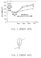
- FIG. 2 shows a temperature profile of a film capacitor during a soldering process and temperature increases at different positions of the film capacitor.
- FIG. 3 shows the positions on one electrode of the film capacitor where a thermal couple for measuring the temperature of the film capacitor is attached.
- the film capacitor uses a copper wire as its lead wires.
- FIG. 3 a side view of the film capacitor 1 with one lead wire 2 is shown.
- the positions where the thermal couple is attached are labeled with a, b, and c.
- the temperature curves 1, II and III in FIG. 2 respectively show the temperature profiles corresponding to the positions a, b and c.
- the temperature profiles (curves I, I, III) in FIG. 2 show that after preheating at 120°C for 90 seconds, the film capacitor I is lifted and then dipped in a soldering tank at 260°C for 7 seconds.
- the temperature at the terminal end b of the film capacitor 1 rises up to about 150°C, in which the terminal end is referred to one end of the lead wire 2 that is attached to the film capacitor.
- the highest operating temperature (for a rated reduction use) of the polypropylene capacitor is 105°C, the polypropylene film of the film capacitor under 150°C will have a large thermal contraction. Thus the capacitance of the film capacitor is reduced under this situation. If the film capacitor is kept in use, the capacitance of the film capacitor would be further reduced. This mechanism will be described below by using a metallized polypropylene film capacitor as an example.
- FIG. 4A shows a perspective appearance of a film capacitor
- FIG. 4B is a perspective view showing an internal structure of the film capacitor
- FIG. 5 is a cross-sectional view showing the internal structure of the film capacitor.
- the film capacitor 1 comprises two metallized films, metallic contacts 5 and lead wires 2, wherein each metallized film includes a film 3 and a metal layer 4 deposited on the film 3. Each film 3 is not fully deposited with the metal layer 4, and a portion of the film is exposed at one side.
- the two metallized films are stacked and then wound in a manner that the exposed portion of the films 3 are arranged in parallel at opposition direction, as shown in FIGs 4B and 5.
- the metallic contacts 5 are formed by respectively spraying metal material onto two side faces of the wound metallized films and the metallic contacts 5 are thus served as electrodes of the film capacitor 1.
- Each metal layer 4 formed on the film 3 would be electrically connected to one metallized contact 5.
- the film 3 is a dielectric film and can use a polypropylene film which thermal contraction is large. Therefore, the metal layers 4 and the film 3 sandwiched therebetween form a capacitor.
- the two lead wires 2 are respectively coupled to the metallic contacts 5, through which the film capacitor can be mounted onto a circuit board.
- a resistance of the film capacitor 1 is a combination of a resistance of the lead wires 2 and the metallic contacts 5, a resistance of the metallic contacts 5 and the films and a resistance of the deposited metal layers 4, etc., which can be represented by a parameter tan ⁇ .
- the parameter tan ⁇ represents a dielectric dissipation factor, which is one of the capacitor properties.
- a dielectric dissipation factor is defined as cotangent of a phase angle or tangent of a loss angle for a dielectric material. Since the metallic contacts 5 are formed by spraying, the thickness of the metallic contacts 5 is not easily controlled to be uniform. Therefore, the resistance between the metallized contact 5 and the film 3 is easily unstable.
- the contact resistance will increase.
- the temperature exceeds 105°C for a long time, the thermal contraction of the polypropylene becomes large, and the adhesion between the films 3 and the metallic contacts 5 becomes worse. Therefore, the resistance of the film capacitor 1 is increased and the contraction is accelerated. Due to the contraction of the polypropylene film, an effective area of the polypropylene film of the film capacitor 1, which is sandwiched between two deposited metal layers 4, is reduced. Thus, the capacitance of the film capacitor is decreased.
- the aforementioned polypropylene film capacitor can be used in a lighting device of a discharge lamp.
- a solution of how to reduce the effects of temperature and heat during the soldering process is a key issue.
- an object of this invention is to provide a safe lighting device for a lamp device, such as a discharge lamp.
- This lighting device is highly reliable, low in cost, and can mitigate any negative impact on the environment.
- the present invention provides a lighting device for a lamp device, such as a discharge lamp.
- the lighting device comprises a circuit board; and film capacitors, packaged on the circuit board by using leadless flow solders.
- each film capacitor comprises polypropylene films and lead wires, and a material of the lead wires has a thermal conductivity lower than a thermal conductivity of copper. Further, terminals and internal materials of the film capacitors are leadless.
- a diameter of the lead wires can be set to 0.6 ⁇ (mm) or less.
- a cross-sectional area can be set to 35mm 2 or less, and a temperature at a terminal end of the lead wires in the film capacitors during a soldering process is 130°C or less.
- the length of the lead wires from the circuit board to the film capacitor is 2mm or more after the film capacitors are packaged onto the circuit board. In this way, the thermal influence during the soldering of the film capacitors can be reduced.
- the film capacitors can be constructed with a combination of a polypropylene film and an aluminum foil.
- the film capacitors can be also constructed with an aluminum-deposited polypropylene film.
- the present invention further provides an illumination apparatus.
- the illumination apparatus comprises a lamp and a lighting device for lighting the lamp.
- the lighting device comprises a circuit board; and film capacitors packaged on the circuit board by using leadless flow solders.
- Each film capacitor comprises polypropylene films and lead wires, and a material of the lead wires has a thermal conductivity lower than a thermal conductivity of copper, and terminals and internal materials of the film capacitors are leadless.
- the present invention further provides an illumination system.
- the illumination system comprises lamps and at least one lighting device for lighting the lamps.
- the lighting device comprises a circuit board and film capacitors packaged on the circuit board by using leadless flow solders.
- Each film capacitor comprises polypropylene films and lead wires, and a material of the lead wires has a thermal conductivity lower than a thermal conductivity of copper, and terminals and internal materials of the film capacitors are leadless.
- the diameter of the lead wires can be set to 0.6 ⁇ (mm) or less.
- a cross-sectional area of each lead wire can be set to 35mm 2 or less, and a temperature at a terminal end of the lead wires in the film capacitors during a soldering process is 130°C or less.
- the length of the lead wires from the circuit board to the film capacitor is 2mm or more after the film capacitors are packaged onto the circuit board. In this way, the thermal influence during the soldering of the film capacitors can be reduced.
- the film capacitors can be constructed with a combination of a polypropylene film and an aluminum foil.
- the film capacitors can be also constructed with an aluminum-deposited polypropylene film.
- a safe lighting device of a discharge lamp can be provided to decrease the temperature applied to the film capacitor during the soldering process. Therefore, for the leadless solder, the capacitance loss against the polypropylene film capacitor due to the soldering heat can be avoided, and the reliability of the film capacitor can be increased. In addition, the cost can be reduced and any negative impact on the environment can be also mitigated.
- FIG. 1 shows a temperature profile of a film capacitor during the soldering process in which temperature is shown to increase at different positions of the film capacitor.
- FIG. 2 shows positions on one electrode of the film capacitor where a thermal couple for measuring the temperature of the film capacitor is attached.
- FIG. 3A shows a perspective appearance of a film capacitor.
- FIG. 3B is a perspective view showing an internal structure of the film capacitor.
- FIG. 4 is a cross-sectional view showing the internal structure of the film capacitor.
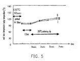
- FIG. 5 shows an experiment result according to the first embodiment of the present invention.
- FIG. 6 is a graph showing a temperature at the terminal end of the capacitor with respect to a cross-sectional area of the capacitor.
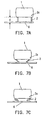
- FIGs. 7A-7C illustrate the forth embodiment of the present invention, showing that the capacitor is mounted on a circuit board or a substrate.
- FIG. 8 is a graph showing the temperature profiles at the terminal end of the film capacitor with respect to a length of the terminal of the film capacitor.
- FIG. 9 is a main circuit diagram of a typical lighting device for a discharge lamp according to the fifth embodiment of the present invention.
- the embodiments of the present invention will be descried in details below.
- the present invention focuses on film capacitors that can be set in a lighting device for a lamp device, such as a discharge lamp. Since the thermal property of the film capacitors is improved as follows, the reliability of the lighting device can be increased.
- the lighting device includes a circuit board and film capacitors packaged on the circuit board by using leadless flow solders.
- Each film capacitor comprises polypropylene films and lead wires, and a material of the lead wires has a thermal conductivity lower than a thermal conductivity of copper. Terminals and internal materials of the film capacitors are free of lead, i.e., all metal portions of the film capacitor are leadless. For example, metal layers deposited on the dielectric films, metallic contacts (used as electrodes), lead wires and lead wire solders, etc.
- FIG. 5 shows an experiment result according to the first embodiment of the present invention.
- FIG. 5 also shows a temperature profile of the film capacitor shown in FIGs. 2-4, wherein the material of the terminals (lead wires) 2 of the film capacitor 1 are changed from copper wires (Cu) to steel wires (Fe).
- the temperature at the terminal end is 150°C.
- a material of the lead wires 2 has a thermal conductivity lower than the thermal conductivity of copper (Cu), and a steel wire is used as an example.
- the temperature at the terminal end can be reduced to 120°C by changing the material of the lead wires 2 from copper wires (Cu) to steel wires (Fe) because the thermal conductivity of the steel wire (Fe) is lower than that of the copper wire (Cu).
- the thermal conductivity of the steel wire (Fe) is only 72 W/m ⁇ K.
- the thermal conductivity of the steel wire (Fe) is about one-fifth of the thermal conductivity of the copper wire (Cu). Therefore, the thermal conduction due to the soldering process can be suppressed.
- circuits can be constructed by using polypropylene film capacitors that are adversely affected by the thermal influence caused by the soldering process. Therefore, by using the above lead wires 2 that are also plated without lead (Pb), a safe lighting device of a discharge lamp, which is also lower in cost and has less adverse effect on the environment, can be provided.
- the second embodiment according to the present is further discussed as follows.
- the thermal conductivity is decreased since the material of the lead wires is changed from Cu to Fe.
- the thermal influence during the soldering process can be further reduced by making the lead diameter smaller.
- a copper wire with a diameter of 0.8 ⁇ is usually used.
- the temperature at the terminal end of the film capacitor can be further reduced by using a steel wire (Fe) with a diameter of 0.6 ⁇ or less.
- a cross-sectional area of the film capacitors can be set to 35mm 2 or less.
- the third embodiment of the present invention is described.
- the film material it self of the film capacitor can be also changed for further improving a thermal property of the film capacitor.
- a high thermal resistant polypropylene is used for the film of the capacitor.
- the highest operating temperature for a fully-rated capacitor is about 85°C.
- the fully-rated means that a voltage, a current and a frequency of the capacitor is operated at its rated value (100%), and the rated reduction means that the voltage, the current and the frequency of the capacitor is operated below its rated value (100%), especially in a high temperature environment.
- the Japanese Laid Open Publication H10-156939 discloses a polypropylene film (a high thermal resistant polypropylene film) or a capacitor using this film to suppress thermal contraction at high temperature, in which the highest operating temperature for the polyproylene film can be further increased.
- the Japanese Laid Open Publication H10-119126 discloses a polypropylene film capable of increasing its highest operating temperature by 20°C
- the Japanese Laid Open Publication H5-217799 discloses a metallized capacitor.
- Table 1 shows a temperature difference at the terminal end of the capacitor due to different capacitor films.
- FIG. 6 is a graph showing a temperature at the terminal end of the capacitor with respect to a cross-sectional area of the capacitor.
- the area of the capacitor means an area of a metallized contact at terminal end of the film capacitor, or an area of an electrode of the capacitor.
- the temperature at the terminal end of the Cu lead wire might exceed the upper limit temperature 125°C when the cross-sectional area is less than 25mm 2 .
- the temperature at the terminal end of a film capacitor with a smaller cross-sectional area can be within the upper limit of 105°C.
- the film capacitor is made by using the high thermal resist polypropylene film and the Fe lead wires, the thermal property of the film capacitor is significantly improved.
- the temperature will exceed 105°C as indicated by the solid line in FIG. 6, which is an upper limit temperature for an ordinary polypropylene film.
- the temperature can be less than 125°C .
- the dash line in FIG. 6 depicts an upper limit temperature for the high thermal resistant polypropylene. Therefore, the soldering thermal resistance can be sufficiently maintained.
- FIGs. 7A-7C illustrate the fourth embodiment of the present invention, showing that the capacitor is mounted on a circuit board or a substrate.
- the bared portion of the lead wires 2 of the capacitor 1 is maintained at 2mm or more. Therefore, a temperature rise at the terminal end of the capacitor can be reduced by 3°C or more during the soldering process.
- FIGs. 7A-7C shows three examples based on the concept of the fourth embodiment. These example are not used to limit the scope of the present invention, other variation can be made under the concept for people skilled in this art.
- FIG. 7A shows the first example of the fourth embodiment.
- the capacitor 1 with the lead wires 2 is vertically mounted on the circuit board 6.
- a gap "d" between the capacitor 1 and the circuit board 6 is 2mm or more. Due to a heat gradient in the gap, a temperature rise at the terminal end can be reduced during the soldering process.
- FIG. 7B shows the second example of the fourth embodiment.
- the lead wires 2 are packaged with the capacitor 1 and extended at an inclination, and are mounted on the circuit board 6 also at an inclination.
- the length of the inclined lead wires 2, i.e., the bared portion of the lead wires 2 is 2mm or more. In this way, a heat gradient is created between the capacitor I and the circuit board 6.
- FIG. 7C shows the third example of the fourth embodiment.
- the lead wires 2 are bent into a crank shape and packaged with the capacitor 1. After the capacitor 1 is mounted to the circuit board 6, the total length of bared portion of the lead wires 2 is kept at 2mm or more. In this way, a heat gradient is created between the capacitor 1 and the circuit board 6. Due to the heat gradient, a temperature rise at the terminal end can be reduced during the soldering process.
- the thermal conductivity of a material is equivalent to the quantity of heat that passes in unit time through unit area of a plate, when its opposite faces are subject to unit temperature gradient (e.g.
- the temperature gradient will change.
- the heat gradient is sufficient to decrease the temperature rise at the terminal end of the film capacitor 1.
- FIG. 8 is a graph showing the temperature profiles at the terminal end of the film capacitor with respect to a length of the terminal of the film capacitor, in which cases the use of the Cu wire and the CP wire as the lead wires are depicted and the cross-section area of the film capacitor is 10mm 2 .
- the soldering condition of the experiment shown in FIG. 8 is preheating at 120°C for 90seconds and soldering dip at 260°C for 7seconds.
- a bold line indicates an upper limit temperature (140°C) at the terminal end of the film capacitor according to a reliability test
- a dash line indicates an upper limit temperature (130°C) at the terminal end of the film capacitor obtained from a margin according to the reliability test data.
- the temperature at the terminal end of the film capacitor with the Cu leads is higher than that with the CP (Fe) leads (the CP (Fe) wire) by about 30°C. Furthermore, for the Cu lead wires, the temperature at the terminal end of the film capacitor is always higher than the upper limit temperature 140°C, even though the lead length is set to 2mm or more. For the CP lead wires, the temperature at the terminal end of the film capacitor is kept below the upper limit temperature 130°C as indicated by the dash line.
- the temperature at the terminal end of the film capacitor is reduced by about 6°C when the lead length on the circuit board is set to 2mm. If the margin is reduced by half, a temperature reduction effect of about 3°C or more per 2mm (lead length) is resulted.
- Table 2 shows a reliability test result according to the temperature at the terminal end of the film capacitor.
- the criteria for judging the electric property is that a variation of the capacitance is within ⁇ 3% and a variation of the dielectric dissipation factor (tan ⁇ ) is 200% or less.
- the heat cycle is 1050 cycles from -40°C to 110°C.
- the mark ' ⁇ X" indicates failure
- the mark "D” indicates a failure of the variation of dielectric tangent (tan ⁇ )
- the mark "C” indicates a failure of the capacitance variation.
- the heat cycle is implemented based on the lifetime of an inverter. From Table 2, when the temperature at the terminal end reaches 145°C or higher, the electric property of the film capacitor after soldering fails. In contrast, the electric property after soldering and the heat cycle is good when the temperature at the terminal end is 140°C or lower. According to the result, the highest temperature during the soldering process is preferably set at 140°C for reliability. However, if considering the nonuniformity of parts and the ambient temperature during the soldering process, a margin of 10°C shall be taken into consideration. Therefore, the highest upper limit temperature during soldering could be set at 130°C. Referring to FIG. 8, if the CP (Fe) wire is used and the upper limit temperature 130°C is set for a lead length of 0mm, the temperature at the terminal end of the film capacitor would be reduced to about 125°C by setting the lead length to 2mm.
- FIG. 9 is a main circuit diagram of a typical lighting device for a discharge lamp of the fifth embodiment of the present invention.
- the discharge lamp can be a fluorescent lamp.
- a lighting device using the aforementioned capacitors are described.
- the lighting device comprises a capacitor C l , a diode bridge DB, a capacitor C2, a chopper circuit 8, capacitors C3 and Ce, an inverter circuit 9, a capacitor C4, a resonant circuit 10 and an inverter control unit 7.
- the chopper circuit consists of an inductor L1, a switch element S3 and a diode D1.
- the inverter circuit consists of switch elements S1, S2.
- the resonant circuit consists of an inductor L2 and a capacitor C5.
- the alternating current (AC) power source AC is filtered by the capacitor C1 and then rectified by the diode bridge DB.
- the rectified AC voltage is further filtered by the capacitor C2 and smoothly increased by the chopper circuit 8.
- the inverter control unit 7 alternatively turns on and off the switch elements S1, S2.
- the discharge lamp FL is lit by the resonant circuit 10.
- the lighting device shown in FIG. 9 is only an example. Any circuit structure of the lighting device can be within the scope of the present invention if the film capacitors of the lighting device has the structure as described in the present invention.
- the capacitor C1, C2 are used as filters, and polyethylene terephthalate film capacitors are generally used.
- metallized polypropylene film capacitors for increasing the thermal resistance are used for the capacitor C1, C2.
- the capacitor C3, Ce are used to smooth the voltage from the chopper circuit.
- metallized polypropylene film capacitors are also used as the capacitor C3, Ce.
- the capacitor C4 is used to cut off a DC component, and can use a metallized polypropylene film capacitor.
- the capacitor C5 is used for the resonant circuit 10.
- the film capacitor can be constructed by a combination an aluminum foil and a polypropylene film, or a metallized polypropylene film capacitor is used.
- the metallized polypropylene film can be an aluminum-deposited film, for example.
- the temperature at the terminal end of the film capacitor during the leadless flow soldering process can be reduced to 130°C or less by using the high thermal resistant polypropylene film or by properly selecting a lead diameter, a lead material and a lead length. Therefore, a capacitance loss due to the heat created in the soldering process and a reduction in the reliability can be avoided.
- the above lighting device of the discharge lamp can be built in illumination apparatus for office or home use, and can be used as a high reliable illumination apparatus.
- a plurality of illumination apparatuses of the present invention can be combined to construct a high reliable illumination system.
Landscapes
- Engineering & Computer Science (AREA)
- Power Engineering (AREA)
- Microelectronics & Electronic Packaging (AREA)
- Manufacturing & Machinery (AREA)
- Fixed Capacitors And Capacitor Manufacturing Machines (AREA)
- Arrangement Of Elements, Cooling, Sealing, Or The Like Of Lighting Devices (AREA)
- Structures For Mounting Electric Components On Printed Circuit Boards (AREA)
Applications Claiming Priority (2)
| Application Number | Priority Date | Filing Date | Title |
|---|---|---|---|
| JP2003425035A JP4360899B2 (ja) | 2003-12-22 | 2003-12-22 | 放電灯点灯装置及び照明器具 |
| EP04801381A EP1698212A2 (de) | 2003-12-22 | 2004-12-15 | Beleuchtungseinrichtung einer entladungslampe, beleuchtungsvorrichtung und beleuchtungssystem |
Related Parent Applications (1)
| Application Number | Title | Priority Date | Filing Date |
|---|---|---|---|
| EP04801381A Division EP1698212A2 (de) | 2003-12-22 | 2004-12-15 | Beleuchtungseinrichtung einer entladungslampe, beleuchtungsvorrichtung und beleuchtungssystem |
Publications (1)
| Publication Number | Publication Date |
|---|---|
| EP1909541A1 true EP1909541A1 (de) | 2008-04-09 |
Family
ID=34736233
Family Applications (3)
| Application Number | Title | Priority Date | Filing Date |
|---|---|---|---|
| EP08003138A Ceased EP1916883A1 (de) | 2003-12-22 | 2004-12-15 | Leuchtgerät für eine Entladungslampe, Beleuchtungsvorrichtung und Beleuchtungssystem |
| EP04801381A Withdrawn EP1698212A2 (de) | 2003-12-22 | 2004-12-15 | Beleuchtungseinrichtung einer entladungslampe, beleuchtungsvorrichtung und beleuchtungssystem |
| EP07021310A Ceased EP1909541A1 (de) | 2003-12-22 | 2004-12-15 | Beleuchtungsvorrichtung einer Entladungslampe, Beleuchtungsvorrichtung und Beleuchtungssystem |
Family Applications Before (2)
| Application Number | Title | Priority Date | Filing Date |
|---|---|---|---|
| EP08003138A Ceased EP1916883A1 (de) | 2003-12-22 | 2004-12-15 | Leuchtgerät für eine Entladungslampe, Beleuchtungsvorrichtung und Beleuchtungssystem |
| EP04801381A Withdrawn EP1698212A2 (de) | 2003-12-22 | 2004-12-15 | Beleuchtungseinrichtung einer entladungslampe, beleuchtungsvorrichtung und beleuchtungssystem |
Country Status (5)
| Country | Link |
|---|---|
| US (1) | US7667975B2 (de) |
| EP (3) | EP1916883A1 (de) |
| JP (1) | JP4360899B2 (de) |
| CN (1) | CN1883237B (de) |
| WO (1) | WO2005064228A2 (de) |
Families Citing this family (6)
| Publication number | Priority date | Publication date | Assignee | Title |
|---|---|---|---|---|
| DE102005043413A1 (de) * | 2005-09-13 | 2007-03-15 | Robert Bosch Gmbh | Grundmodul für einen Bewegungssensor |
| JP5518289B2 (ja) * | 2007-12-17 | 2014-06-11 | 株式会社コマデン | 吊下式照明具及び導線 |
| US8619409B2 (en) | 2008-10-01 | 2013-12-31 | Taiyo Yuden Co., Ltd. | Electrochemical device |
| US20120019985A1 (en) * | 2010-07-20 | 2012-01-26 | Lien Chang Electronic Enterprise Co., Ltd. | Aluminum electrolyte capacitor |
| US8149589B2 (en) * | 2010-08-19 | 2012-04-03 | Lien Chang Electronic Enterprise Co., Ltd. | Capacitor holder |
| JP2014035626A (ja) * | 2012-08-08 | 2014-02-24 | Wacom Co Ltd | 電子回路及び位置指示器 |
Citations (6)
| Publication number | Priority date | Publication date | Assignee | Title |
|---|---|---|---|---|
| US4158218A (en) * | 1977-09-19 | 1979-06-12 | Union Carbide Corporation | Ceramic capacitor device |
| US4578737A (en) * | 1983-06-03 | 1986-03-25 | Wolfgang Westermann | Synthetic resin film wound capacitor |
| DE3929791A1 (de) * | 1989-09-07 | 1991-03-21 | Roederstein Kondensatoren | Kondensator mit metallisierten kunststoffolien |
| WO2001097572A1 (en) * | 2000-06-12 | 2001-12-20 | Matsushita Electric Works, Ltd. | Electronic ballast for a discharge lamp |
| EP1263270A2 (de) * | 2001-06-01 | 2002-12-04 | Nec Corporation | Verfahren zur Bestückung von elektronischen Bauteilen ohne Bildung von unnötigen Lötkugeln |
| US20030011319A1 (en) * | 1999-12-27 | 2003-01-16 | Tridonicatco Gmbh & Co. Kg | Electronic ballast and electronic transformer |
Family Cites Families (23)
| Publication number | Priority date | Publication date | Assignee | Title |
|---|---|---|---|---|
| JPS5937847B2 (ja) * | 1978-02-06 | 1984-09-12 | ニッセイ電機株式会社 | プラスチツクフイルムコンデンサ |
| US4534032A (en) * | 1982-09-30 | 1985-08-06 | Metalworking Lasers International Ltd. | Apparatus for establishing and maintaining a stable electrical discharge across a stream of gas, and a high-power laser including such apparatus |
| JPS622512A (ja) * | 1985-06-27 | 1987-01-08 | 松下電器産業株式会社 | 金属化プラスチツクフイルムコンデンサ |
| US4646197A (en) * | 1985-12-23 | 1987-02-24 | Supercon, Inc. | Tantalum capacitor lead wire |
| JPH0442906Y2 (de) * | 1986-06-30 | 1992-10-12 | ||
| JPH0519942Y2 (de) * | 1986-09-30 | 1993-05-25 | ||
| JPH079865B2 (ja) * | 1987-02-09 | 1995-02-01 | 東レ株式会社 | 無外装ポリエステルフイルムコンデンサ |
| JPH05217799A (ja) | 1992-01-31 | 1993-08-27 | Toyo Condenser Kk | 蒸着金属化フィルムコンデンサ |
| JPH08329791A (ja) | 1995-05-29 | 1996-12-13 | Fujitsu Ltd | マトリックスボード |
| JPH08329731A (ja) * | 1995-05-31 | 1996-12-13 | Tec Corp | 電気機器 |
| JPH0950934A (ja) * | 1995-08-07 | 1997-02-18 | Hitachi Aic Inc | プラスチックフィルムコンデンサ |
| JPH0982562A (ja) * | 1995-09-19 | 1997-03-28 | Matsushita Electric Ind Co Ltd | 金属化フィルムコンデンサ |
| JPH10156939A (ja) | 1996-10-04 | 1998-06-16 | Toray Ind Inc | ポリプロピレンフィルムおよびコンデンサー |
| JP3799685B2 (ja) | 1996-10-17 | 2006-07-19 | 東レ株式会社 | 金属化二軸配向ポリプロピレンフィルムおよびコンデンサー |
| DE19710963C1 (de) * | 1997-03-17 | 1998-09-17 | Wolfgang Westermann | SMD-Folienkondensator |
| JP2000173855A (ja) * | 1998-12-10 | 2000-06-23 | Mitsubishi Polyester Film Copp | コンデンサー用ポリエチレン−2,6−ナフタレートフィルム |
| JP2001230151A (ja) * | 2000-02-16 | 2001-08-24 | Matsushita Electric Ind Co Ltd | リードレスチップ部品 |
| JP3923840B2 (ja) * | 2001-04-11 | 2007-06-06 | 株式会社三浦合金工業所 | 金属化プラスチックフィルムコンデンサの外部電極用無鉛合金 |
| JP3847136B2 (ja) * | 2001-10-29 | 2006-11-15 | 京セラ株式会社 | 電子部品 |
| JP2003243597A (ja) * | 2002-02-20 | 2003-08-29 | Nec Electronics Corp | 電子部品及びその製造方法 |
| JPWO2004084242A1 (ja) * | 2003-03-19 | 2006-06-29 | 東レ株式会社 | 扁平型コンデンサ用ポリプロピレンフィルム及びそれからなる扁平型コンデンサ |
| JP2004356208A (ja) * | 2003-05-27 | 2004-12-16 | Shinetsu Film Kk | オールフィルム製電子レンジ用油浸コンデンサーおよびその製造方法 |
| DE10347568A1 (de) * | 2003-10-14 | 2005-05-12 | Degussa | Kondensator mit keramischer Separationsschicht |
-
2003
- 2003-12-22 JP JP2003425035A patent/JP4360899B2/ja not_active Expired - Fee Related
-
2004
- 2004-12-15 EP EP08003138A patent/EP1916883A1/de not_active Ceased
- 2004-12-15 EP EP04801381A patent/EP1698212A2/de not_active Withdrawn
- 2004-12-15 CN CN2004800341208A patent/CN1883237B/zh not_active Expired - Fee Related
- 2004-12-15 US US10/580,071 patent/US7667975B2/en not_active Expired - Fee Related
- 2004-12-15 EP EP07021310A patent/EP1909541A1/de not_active Ceased
- 2004-12-15 WO PCT/IB2004/004120 patent/WO2005064228A2/en not_active Ceased
Patent Citations (6)
| Publication number | Priority date | Publication date | Assignee | Title |
|---|---|---|---|---|
| US4158218A (en) * | 1977-09-19 | 1979-06-12 | Union Carbide Corporation | Ceramic capacitor device |
| US4578737A (en) * | 1983-06-03 | 1986-03-25 | Wolfgang Westermann | Synthetic resin film wound capacitor |
| DE3929791A1 (de) * | 1989-09-07 | 1991-03-21 | Roederstein Kondensatoren | Kondensator mit metallisierten kunststoffolien |
| US20030011319A1 (en) * | 1999-12-27 | 2003-01-16 | Tridonicatco Gmbh & Co. Kg | Electronic ballast and electronic transformer |
| WO2001097572A1 (en) * | 2000-06-12 | 2001-12-20 | Matsushita Electric Works, Ltd. | Electronic ballast for a discharge lamp |
| EP1263270A2 (de) * | 2001-06-01 | 2002-12-04 | Nec Corporation | Verfahren zur Bestückung von elektronischen Bauteilen ohne Bildung von unnötigen Lötkugeln |
Also Published As
| Publication number | Publication date |
|---|---|
| EP1916883A1 (de) | 2008-04-30 |
| US20070103879A1 (en) | 2007-05-10 |
| WO2005064228A2 (en) | 2005-07-14 |
| CN1883237B (zh) | 2011-10-12 |
| JP4360899B2 (ja) | 2009-11-11 |
| EP1698212A2 (de) | 2006-09-06 |
| JP2005183288A (ja) | 2005-07-07 |
| CN1883237A (zh) | 2006-12-20 |
| US7667975B2 (en) | 2010-02-23 |
| WO2005064228A3 (en) | 2006-03-23 |
Similar Documents
| Publication | Publication Date | Title |
|---|---|---|
| US11410816B2 (en) | Multilayer ceramic electronic component including metal terminals connected to outer electrodes | |
| US11501921B2 (en) | Multilayer ceramic electronic component | |
| US10692655B2 (en) | Filter component for filtering an interference signal | |
| CN114566384A (zh) | 多层电容器 | |
| US11527364B2 (en) | Multilayer ceramic electronic component including a plurality of bodies and metal terminals connected to outer electrodes | |
| CN104578753B (zh) | 复合电子组件和其上安装有复合电子组件的板 | |
| US7667975B2 (en) | Lighting device of discharge lamp, illumination apparatus and illumination system | |
| US10115523B2 (en) | Ceramic electronic component and mounting structure of the same | |
| US20160012957A1 (en) | Chip coil component | |
| KR101813365B1 (ko) | 적층형 커패시터 및 그 실장 기판 | |
| TW202042259A (zh) | 積層陶瓷電子零件及電路基板 | |
| CN116420208A (zh) | 金属化薄膜以及薄膜电容器 | |
| Anderson | Select the right plastic film capacitor for your power electronic applications | |
| HK1095694A (en) | Lighting device of discharge lamp, illumination apparatus and illumination system | |
| JP4361101B2 (ja) | 放電灯点灯装置及び照明器具 | |
| KR100302106B1 (ko) | 두개의강화층을갖는콘덴서용금속증착필름및그제조방법 | |
| JP4296532B2 (ja) | コンデンサ用蒸着フィルム及びそれを用いたコンデンサ | |
| DE102017105351B4 (de) | Leistungshalbleitermodul mit Leistungshalbleiterbauelementen und einem Kondensator | |
| US20250218683A1 (en) | Multilayer electronic component | |
| JP2010040633A (ja) | フィルムコンデンサ | |
| JP2005252141A (ja) | 電子部品及びその製造方法 | |
| EP3837743A1 (de) | Verwendung einer metallkern-leiterplatte (pcb) zur erzeugung eines ultraschmalen hochstrompulstreibers | |
| JP5304325B2 (ja) | コンデンサモジュール | |
| JP2005222910A (ja) | 放電灯点灯装置及び照明器具 | |
| JPH03241804A (ja) | チップ形金属化フィルムコンデンサ |
Legal Events
| Date | Code | Title | Description |
|---|---|---|---|
| PUAI | Public reference made under article 153(3) epc to a published international application that has entered the european phase |
Free format text: ORIGINAL CODE: 0009012 |
|
| 17P | Request for examination filed |
Effective date: 20071031 |
|
| AC | Divisional application: reference to earlier application |
Ref document number: 1698212 Country of ref document: EP Kind code of ref document: P |
|
| AK | Designated contracting states |
Kind code of ref document: A1 Designated state(s): AT BE BG CH CY CZ DE DK EE ES FI FR GB GR HU IE IS IT LI LT LU MC NL PL PT RO SE SI SK TR |
|
| AX | Request for extension of the european patent |
Extension state: AL BA HR LV MK YU |
|
| 17Q | First examination report despatched |
Effective date: 20080617 |
|
| AKX | Designation fees paid |
Designated state(s): DE |
|
| RAP1 | Party data changed (applicant data changed or rights of an application transferred) |
Owner name: PANASONIC ELECTRIC WORKS CO., LTD. |
|
| APBK | Appeal reference recorded |
Free format text: ORIGINAL CODE: EPIDOSNREFNE |
|
| APBN | Date of receipt of notice of appeal recorded |
Free format text: ORIGINAL CODE: EPIDOSNNOA2E |
|
| APBR | Date of receipt of statement of grounds of appeal recorded |
Free format text: ORIGINAL CODE: EPIDOSNNOA3E |
|
| APAZ | Date of receipt of statement of grounds of appeal deleted |
Free format text: ORIGINAL CODE: EPIDOSDNOA3E |
|
| APBR | Date of receipt of statement of grounds of appeal recorded |
Free format text: ORIGINAL CODE: EPIDOSNNOA3E |
|
| APAF | Appeal reference modified |
Free format text: ORIGINAL CODE: EPIDOSCREFNE |
|
| APAF | Appeal reference modified |
Free format text: ORIGINAL CODE: EPIDOSCREFNE |
|
| RAP1 | Party data changed (applicant data changed or rights of an application transferred) |
Owner name: PANASONIC CORPORATION |
|
| APBT | Appeal procedure closed |
Free format text: ORIGINAL CODE: EPIDOSNNOA9E |
|
| STAA | Information on the status of an ep patent application or granted ep patent |
Free format text: STATUS: THE APPLICATION HAS BEEN REFUSED |
|
| 18R | Application refused |
Effective date: 20081229 |