EP1976018A2 - Transistor à effet de champ à couche mince et affichage - Google Patents
Transistor à effet de champ à couche mince et affichage Download PDFInfo
- Publication number
- EP1976018A2 EP1976018A2 EP08005583A EP08005583A EP1976018A2 EP 1976018 A2 EP1976018 A2 EP 1976018A2 EP 08005583 A EP08005583 A EP 08005583A EP 08005583 A EP08005583 A EP 08005583A EP 1976018 A2 EP1976018 A2 EP 1976018A2
- Authority
- EP
- European Patent Office
- Prior art keywords
- active layer
- electric resistance
- field effect
- layer
- thin film
- Prior art date
- Legal status (The legal status is an assumption and is not a legal conclusion. Google has not performed a legal analysis and makes no representation as to the accuracy of the status listed.)
- Granted
Links
Images


Classifications
-
- G—PHYSICS
- G02—OPTICS
- G02F—OPTICAL DEVICES OR ARRANGEMENTS FOR THE CONTROL OF LIGHT BY MODIFICATION OF THE OPTICAL PROPERTIES OF THE MEDIA OF THE ELEMENTS INVOLVED THEREIN; NON-LINEAR OPTICS; FREQUENCY-CHANGING OF LIGHT; OPTICAL LOGIC ELEMENTS; OPTICAL ANALOGUE/DIGITAL CONVERTERS
- G02F1/00—Devices or arrangements for the control of the intensity, colour, phase, polarisation or direction of light arriving from an independent light source, e.g. switching, gating or modulating; Non-linear optics
- G02F1/01—Devices or arrangements for the control of the intensity, colour, phase, polarisation or direction of light arriving from an independent light source, e.g. switching, gating or modulating; Non-linear optics for the control of the intensity, phase, polarisation or colour
- G02F1/13—Devices or arrangements for the control of the intensity, colour, phase, polarisation or direction of light arriving from an independent light source, e.g. switching, gating or modulating; Non-linear optics for the control of the intensity, phase, polarisation or colour based on liquid crystals, e.g. single liquid crystal display cells
- G02F1/133—Constructional arrangements; Operation of liquid crystal cells; Circuit arrangements
- G02F1/136—Liquid crystal cells structurally associated with a semi-conducting layer or substrate, e.g. cells forming part of an integrated circuit
-
- H—ELECTRICITY
- H10—SEMICONDUCTOR DEVICES; ELECTRIC SOLID-STATE DEVICES NOT OTHERWISE PROVIDED FOR
- H10D—INORGANIC ELECTRIC SEMICONDUCTOR DEVICES
- H10D30/00—Field-effect transistors [FET]
- H10D30/60—Insulated-gate field-effect transistors [IGFET]
- H10D30/67—Thin-film transistors [TFT]
- H10D30/674—Thin-film transistors [TFT] characterised by the active materials
- H10D30/6755—Oxide semiconductors, e.g. zinc oxide, copper aluminium oxide or cadmium stannate
-
- H—ELECTRICITY
- H10—SEMICONDUCTOR DEVICES; ELECTRIC SOLID-STATE DEVICES NOT OTHERWISE PROVIDED FOR
- H10D—INORGANIC ELECTRIC SEMICONDUCTOR DEVICES
- H10D30/00—Field-effect transistors [FET]
- H10D30/60—Insulated-gate field-effect transistors [IGFET]
- H10D30/67—Thin-film transistors [TFT]
- H10D30/6704—Thin-film transistors [TFT] having supplementary regions or layers in the thin films or in the insulated bulk substrates for controlling properties of the device
- H10D30/6706—Thin-film transistors [TFT] having supplementary regions or layers in the thin films or in the insulated bulk substrates for controlling properties of the device for preventing leakage current
-
- H—ELECTRICITY
- H10—SEMICONDUCTOR DEVICES; ELECTRIC SOLID-STATE DEVICES NOT OTHERWISE PROVIDED FOR
- H10D—INORGANIC ELECTRIC SEMICONDUCTOR DEVICES
- H10D30/00—Field-effect transistors [FET]
- H10D30/60—Insulated-gate field-effect transistors [IGFET]
- H10D30/67—Thin-film transistors [TFT]
- H10D30/6704—Thin-film transistors [TFT] having supplementary regions or layers in the thin films or in the insulated bulk substrates for controlling properties of the device
- H10D30/6713—Thin-film transistors [TFT] having supplementary regions or layers in the thin films or in the insulated bulk substrates for controlling properties of the device characterised by the properties of the source or drain regions, e.g. compositions or sectional shapes
-
- H—ELECTRICITY
- H10—SEMICONDUCTOR DEVICES; ELECTRIC SOLID-STATE DEVICES NOT OTHERWISE PROVIDED FOR
- H10D—INORGANIC ELECTRIC SEMICONDUCTOR DEVICES
- H10D30/00—Field-effect transistors [FET]
- H10D30/60—Insulated-gate field-effect transistors [IGFET]
- H10D30/67—Thin-film transistors [TFT]
- H10D30/6757—Thin-film transistors [TFT] characterised by the structure of the channel, e.g. transverse or longitudinal shape or doping profile
Definitions
- FPDs are driven by an active matrix circuit including field effect-type thin film transistors each using, as an active layer, an amorphous silicon thin film or a polycrystalline silicon thin film provided on a glass substrate.
- an active matrix circuit including field effect-type thin film transistors each using, as an active layer, an amorphous silicon thin film or a polycrystalline silicon thin film provided on a glass substrate.
- the field effect-type thin film transistor is sometimes referred to as a "thin film transistor" or "TFT”.
- the present invention has been made in view of the above circumstances and provides a thin film field effect transistor and a display using the same with the following aspects.
- the electric conductivity of the active layer is preferably 10 -1 Scm -1 or more and less than 10 2 Scm -1 .
- the substrate is a flexible resin substrate.
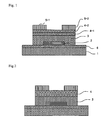
- the active layer 4-11 (which is a high-electric conductivity layer) borders on the gate insulating layer 13, and the electric resistance layer 4-12 (which is a low-electric conductivity layer) borders on the source electrode 5-11 and the drain electrode 5-12.
- the compositions of the active layer 4-11 and electric resistance layer 4-12 are determined so that the electric conductivity of the active layer 4-11 is higher than that of the electric resistance layer 4-12 when no voltage is applied to the gate electrode.
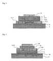
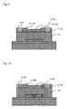
- Fig. 8 is a schematic diagram showing a reversed stagger structure as another example of the thin film field effect transistor according to the invention.
- An active layer 4-41 is formed on a gate insulating layer 43, and an electric resistance layer 4-42 is stacked on the active layer 4-41.
- the electric resistance layer 4-42 is subjected to patterning so that the electric resistance layer 4-42 is formed only in the area corresponding to the place where a source electrode 5-41 is to be provided.
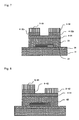
- the field effect mobility of the transistor is made higher and thus a high ON current can be obtained because the active layer 4-61 which becomes the channel has high electric conductivity.
- the electric resistance layer 4-62 which has high electric resistance keeps the OFF current low.
- the ON-OFF ratio is remarkably improved.
- the source electrode 5-61 and drain electrode 5-62 in the structure shown in Fig. 10 may be interchanged, of course; in this case, the drain electrode 5-62 is connected with the electric resistance layer 4-62.
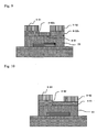
- Fig. 11 is a schematic diagram showing a top gate structure which is another example of the thin film field effect transistor according to the invention.
- electric resistance layers 4-72a and 4-72b, and an active layer 4-71 are formed on an insulating layer 76.
- the electric resistance layers 4-72a and 4-72b are formed by patterning so as to lie in the areas corresponding to the places where a source electrode 5-71 and a drain electrode 5-72 are to be provided.
- the active layer 4-71 is formed by patterning so as to be located in an area other than the places where the electric resistance layers 4-72a and 4-72b are disposed. According to this arrangement, the active layer 4-71 is electrically connected to the source electrodes 5-71 and the drain electrode 5-72 not directly, but indirectly through the electric resistance layers 4-72a and 4-72b.
- Fig. 13 is a schematic diagram showing an example of top gate structure which is another example of the thin film field effect transistor according to the invention.
- electric resistance layers 4-92a and 4-92b, and an active layer 4-91 are formed by patterning so that they are arrayed, in a direction parallel with a surface of a substrate in the order of a source electrode 5-91, the electric resistance layer 4-92a, the active layer 4-91, the electric resistance layer 4-92b, and a drain electrode 5-92.
- the active layer 4-91 is electrically connected to the source electrode 5-91 and the drain electrode 5-92 not directly, but indirectly through the electric resistance layers 4-92a and 4-92b.
- Fig. 16 is a schematic diagram showing, as an example of the reversed stagger structure, another structure of the thin film field effect transistor according to the invention.
- an electric resistance layer 4-122 and an active layer 4-121 are formed by patterning so that they are arrayed, in a direction parallel with a surface of a substrate, in the order of a source electrode 5-121, the electric resistance layer 4-122, the active layer 4-121, and a drain electrode 5-122.
- the active layer 4-121 is electrically connected to the source electrode 5-121 not directly, but indirectly through the electric resistance layer 4-122.
- an insulator such as SiO 2 , SiN x , SiON, Al 2 O 3 , Y 2 O 3 , Ta 2 O 5 , HfO 2 and the like, or a mixed crystal compound containing at least two of these is used.
- a polymeric insulator such as polyimide may be used for the gate insulating layer.
- oxide semiconductors but also inorganic semiconductors such as Si and Ge, compound semiconductors such as GaAs, and organic semiconductor materials such as pentacene, polythiophene, and carbon nanotube, and the like can be used for the active layer and the electric resistance layer.
- inorganic semiconductors such as Si and Ge
- compound semiconductors such as GaAs
- organic semiconductor materials such as pentacene, polythiophene, and carbon nanotube, and the like can be used for the active layer and the electric resistance layer.
- the active layer of the invention is characterized in that it is near the gate insulating layer, and the electric conductivity thereof is higher than that of the electric resistance layer which is near the source electrode and the drain electrode.
- the ratio of the electric conductivity of the active layer to the electric conductivity of the electric resistance layer is preferably from 10 1 to 10 10 , and more preferably from 10 2 to 10 8 .
- the electric conductivity of the active layer is preferably 10 -4 Scm -1 or more and less than 10 2 Scm -1 , and more preferably 10 -1 Scm -1 or more and less than 10 2 Scm -1 .
- the means stated in the above (1) to (4) may be used independently or in combination.
- the resultant film is an amorphous film.
- the thickness of the gate electrode is preferably from 10 nm to 1000 nm.
- the substrate used herein is not particularly limited.
- the following materials are for example suitable for the substrate: inorganic materials such as YSZ (zirconia stabilized yttrium) and glass; and organic materials including polyesters such as polyethylene terephthalate, polybutylene terephthalate and polyethylene naphthalate, and synthetic resins such as polystyrene, polycarbonate, polyether sulfone, polyarylate, allyl diglycol carbonate, polyimide, polycycloolefin, norbornene resin, and polychlorotrifluoroethylene.
- inorganic materials such as YSZ (zirconia stabilized yttrium) and glass
- organic materials including polyesters such as polyethylene terephthalate, polybutylene terephthalate and polyethylene naphthalate, and synthetic resins such as polystyrene, polycarbonate, polyether sulfone, polyarylate, allyl diglycol carbonate, polyimide,
- a flexible substrate As for the material used for the flexible substrate, an organic plastic film which has high transmittance is preferable.
- the following materials can be used: polyesters such as polyethylene terephthalate, polybutylene phthalate and polyethylene naphthalate; and plastic films such as polystyrene, polycarbonate, polyether sulfone, polyarylate, polyimide; polycycloolefin, norbornene resin, and polychlorotrifluoroethylene.
- a method for forming the protective insulating film there is no particular limitation as to a method for forming the protective insulating film.
- a vacuum deposition method a sputtering method, a reactive sputtering method, an MBE (molecular beam epitaxial) method, a cluster ion beam method, an ion plating method, a plasma polymerization method (high-frequency excitation ion plating method), a plasma CVD method, a laser CVD method, a thermal CVD method, a gas source CVD method, a coating method, a printing method, or a transfer method may be applied.
- a vacuum deposition method a sputtering method, a reactive sputtering method, an MBE (molecular beam epitaxial) method, a cluster ion beam method, an ion plating method, a plasma polymerization method (high-frequency excitation ion plating method), a plasma CVD method, a laser CVD method, a thermal CV
- RF magnetron sputtering vacuum deposition was performed under conditions similar to Condition 1 except that the O 2 flow rate was changed to 1.8 sccm.
- the ON-OFF ratios were determined from the TFT transfer characteristics; specifically, from the ratio of the maximum value Id max of the drain current Id to the minimum value Id min of the drain current Id, i.e., Id max /Id min .
- the Device No. 4 was evaluated with respect to TFT device performance in a manner similar to Example 1. Results of the evaluation are presented in Table 2.
Landscapes
- Physics & Mathematics (AREA)
- Nonlinear Science (AREA)
- Optics & Photonics (AREA)
- Thin Film Transistor (AREA)
- Chemical & Material Sciences (AREA)
- Crystallography & Structural Chemistry (AREA)
- Microelectronics & Electronic Packaging (AREA)
- General Physics & Mathematics (AREA)
- Engineering & Computer Science (AREA)
- Mathematical Physics (AREA)
- Liquid Crystal (AREA)
- Electroluminescent Light Sources (AREA)
- Dram (AREA)
- Devices For Indicating Variable Information By Combining Individual Elements (AREA)
- Inorganic Compounds Of Heavy Metals (AREA)
- Physical Vapour Deposition (AREA)
Applications Claiming Priority (2)
| Application Number | Priority Date | Filing Date | Title |
|---|---|---|---|
| JP2007082859 | 2007-03-27 | ||
| JP2008025619 | 2008-02-05 |
Publications (3)
| Publication Number | Publication Date |
|---|---|
| EP1976018A2 true EP1976018A2 (fr) | 2008-10-01 |
| EP1976018A3 EP1976018A3 (fr) | 2011-05-11 |
| EP1976018B1 EP1976018B1 (fr) | 2013-05-08 |
Family
ID=39577862
Family Applications (1)
| Application Number | Title | Priority Date | Filing Date |
|---|---|---|---|
| EP08005583.3A Active EP1976018B1 (fr) | 2007-03-27 | 2008-03-26 | Transistor à effet de champ à couche mince et affichage |
Country Status (4)
| Country | Link |
|---|---|
| US (1) | US8178926B2 (fr) |
| EP (1) | EP1976018B1 (fr) |
| JP (3) | JP4727684B2 (fr) |
| KR (2) | KR101477804B1 (fr) |
Cited By (26)
| Publication number | Priority date | Publication date | Assignee | Title |
|---|---|---|---|---|
| WO2011013596A1 (fr) * | 2009-07-31 | 2011-02-03 | Semiconductor Energy Laboratory Co., Ltd. | Dispositif à semi-conducteur et son procédé de fabrication |
| WO2011013523A1 (fr) * | 2009-07-31 | 2011-02-03 | Semiconductor Energy Laboratory Co., Ltd. | Dispositif semi-conducteur et procédé de fabrication de celui-ci |
| EP2346082A1 (fr) * | 2010-01-15 | 2011-07-20 | Samsung Electronics Co., Ltd. | Transistors, procédés de fabrication d'un transistor et dispositifs électroniques incluant un transistor |
| EP2423966A1 (fr) * | 2008-12-12 | 2012-02-29 | Canon Kabushiki Kaisha | Transistor à effet de champ et appareil d'affichage |
| US8373203B2 (en) | 2009-11-27 | 2013-02-12 | Semiconductor Energy Laboratory Co., Ltd. | Semiconductor device |
| US8440510B2 (en) | 2010-05-14 | 2013-05-14 | Semiconductor Energy Laboratory Co., Ltd. | Method for manufacturing semiconductor device |
| KR20130139379A (ko) * | 2008-11-07 | 2013-12-20 | 가부시키가이샤 한도오따이 에네루기 켄큐쇼 | 반도체 장치의 제작 방법 |
| US20140030846A1 (en) * | 2008-11-28 | 2014-01-30 | Semiconductor Energy Laboratory Co., Ltd. | Semiconductor device and method for manufacturing the same |
| JP2015128165A (ja) * | 2008-10-03 | 2015-07-09 | 株式会社半導体エネルギー研究所 | 酸化物半導体層 |
| US20170040181A1 (en) | 2010-03-05 | 2017-02-09 | Semiconductor Energy Laboratory Co., Ltd. | Semiconductor device and manufacturing method thereof |
| US9613964B2 (en) | 2010-02-26 | 2017-04-04 | Semiconductor Energy Laboratory Co., Ltd. | Semiconductor device including a memory cell |
| US9627198B2 (en) | 2009-10-05 | 2017-04-18 | Semiconductor Energy Laboratory Co., Ltd. | Method for manufacturing thin film semiconductor device |
| US9748436B2 (en) | 2009-11-27 | 2017-08-29 | Semiconductor Energy Laboratory Co., Ltd. | Semiconductor device and method for manufacturing the same |
| US9837544B2 (en) | 2010-07-02 | 2017-12-05 | Semiconductor Energy Laboratory Co., Ltd. | Semiconductor device having an oxide semiconductor layer |
| US9842942B2 (en) | 2008-10-31 | 2017-12-12 | Semiconductor Energy Laboratory Co., Ltd. | Semiconductor device and method for manufacturing the same |
| US9929280B2 (en) | 2011-03-28 | 2018-03-27 | Semiconductor Energy Laboratory Co., Ltd. | Semiconductor device including oxide semiconductor film containing indium |
| US10014414B2 (en) | 2013-02-28 | 2018-07-03 | Semiconductor Energy Laboratory Co., Ltd. | Semiconductor device and method for manufacturing the same |
| US10089946B2 (en) | 2010-01-20 | 2018-10-02 | Semiconductor Energy Laboratory Co., Ltd. | Display device |
| US10256254B2 (en) | 2009-12-18 | 2019-04-09 | Semiconductor Energy Laboratory Co., Ltd. | Liquid crystal display device and electronic device |
| US10269835B2 (en) | 2012-12-03 | 2019-04-23 | Semiconductor Energy Laboratory Co., Ltd. | Semiconductor device and manufacturing method thereof |
| US10310348B2 (en) | 2009-10-16 | 2019-06-04 | Semiconductor Energy Laboratory Co., Ltd. | Liquid crystal display device and electronic apparatus having the same |
| US10367006B2 (en) | 2008-10-03 | 2019-07-30 | Semiconductor Energy Laboratory Co., Ltd. | Display Device |
| US10516055B2 (en) | 2009-11-13 | 2019-12-24 | Semiconductor Energy Laboratory Co., Ltd. | Semiconductor device and manufacturing method thereof |
| US10566459B2 (en) | 2009-10-30 | 2020-02-18 | Semiconductor Energy Laboratory Co., Ltd. | Semiconductor device having a first region comprising silicon, oxygen and at least one metal element formed between an oxide semiconductor layer and an insulating layer |
| US10804409B2 (en) | 2009-12-11 | 2020-10-13 | Semiconductor Energy Laboratory Co., Ltd. | Semiconductor device and method for manufacturing the same |
| US11417754B2 (en) | 2009-06-30 | 2022-08-16 | Semiconductor Energy Laboratory Co., Ltd. | Method for manufacturing semiconductor device |
Families Citing this family (108)
| Publication number | Priority date | Publication date | Assignee | Title |
|---|---|---|---|---|
| JP3217137B2 (ja) * | 1992-07-28 | 2001-10-09 | 株式会社日立製作所 | 映像信号記録装置、再生装置及び伝送装置 |
| KR100998527B1 (ko) | 2004-11-10 | 2010-12-07 | 고쿠리츠다이가쿠호진 토쿄고교 다이가꾸 | 비정질 산화물 및 전계 효과 트랜지스터 |
| JP4609797B2 (ja) * | 2006-08-09 | 2011-01-12 | Nec液晶テクノロジー株式会社 | 薄膜デバイス及びその製造方法 |
| JP2008276212A (ja) * | 2007-04-05 | 2008-11-13 | Fujifilm Corp | 有機電界発光表示装置 |
| JP2009130209A (ja) * | 2007-11-26 | 2009-06-11 | Fujifilm Corp | 放射線撮像素子 |
| JP4555358B2 (ja) * | 2008-03-24 | 2010-09-29 | 富士フイルム株式会社 | 薄膜電界効果型トランジスタおよび表示装置 |
| KR100941850B1 (ko) * | 2008-04-03 | 2010-02-11 | 삼성모바일디스플레이주식회사 | 박막 트랜지스터, 그의 제조 방법 및 박막 트랜지스터를구비하는 평판 표시 장치 |
| KR101496150B1 (ko) * | 2008-08-19 | 2015-02-27 | 삼성전자주식회사 | 산화물 반도체 및 이를 포함하는 박막 트랜지스터 |
| KR101657957B1 (ko) | 2008-09-12 | 2016-09-20 | 가부시키가이샤 한도오따이 에네루기 켄큐쇼 | 표시 장치 |
| KR101652693B1 (ko) | 2008-10-03 | 2016-09-01 | 가부시키가이샤 한도오따이 에네루기 켄큐쇼 | 표시 장치 |
| US8187919B2 (en) | 2008-10-08 | 2012-05-29 | Lg Display Co. Ltd. | Oxide thin film transistor and method of fabricating the same |
| KR101298611B1 (ko) * | 2008-10-08 | 2013-08-26 | 엘지디스플레이 주식회사 | 산화물 박막 트랜지스터 및 그 제조방법 |
| KR101322314B1 (ko) * | 2008-10-10 | 2013-10-25 | 엘지디스플레이 주식회사 | 산화물 박막 트랜지스터의 제조방법 |
| KR101525590B1 (ko) * | 2008-10-08 | 2015-06-04 | 삼성디스플레이 주식회사 | 표시 기판 및 이의 제조 방법 |
| KR101586674B1 (ko) * | 2008-10-28 | 2016-01-20 | 엘지디스플레이 주식회사 | 산화물 박막 트랜지스터의 제조방법 |
| TWI574423B (zh) | 2008-11-07 | 2017-03-11 | 半導體能源研究所股份有限公司 | 半導體裝置和其製造方法 |
| TWI656645B (zh) | 2008-11-13 | 2019-04-11 | 日商半導體能源研究所股份有限公司 | 半導體裝置及其製造方法 |
| JP2010153802A (ja) * | 2008-11-20 | 2010-07-08 | Semiconductor Energy Lab Co Ltd | 半導体装置及び半導体装置の作製方法 |
| KR101648927B1 (ko) | 2009-01-16 | 2016-08-17 | 가부시키가이샤 한도오따이 에네루기 켄큐쇼 | 반도체 장치 및 그 제작 방법 |
| JP5210187B2 (ja) | 2009-01-22 | 2013-06-12 | ユー・ディー・シー アイルランド リミテッド | 有機電界発光素子 |
| US8492756B2 (en) | 2009-01-23 | 2013-07-23 | Semiconductor Energy Laboratory Co., Ltd. | Semiconductor device and method for manufacturing the same |
| US8367486B2 (en) | 2009-02-05 | 2013-02-05 | Semiconductor Energy Laboratory Co., Ltd. | Transistor and method for manufacturing the transistor |
| JP5504008B2 (ja) | 2009-03-06 | 2014-05-28 | 株式会社半導体エネルギー研究所 | 半導体装置 |
| JP2010245366A (ja) * | 2009-04-08 | 2010-10-28 | Fujifilm Corp | 電子素子及びその製造方法、並びに表示装置 |
| TWI476917B (zh) | 2009-04-16 | 2015-03-11 | 半導體能源研究所股份有限公司 | 半導體裝置和其製造方法 |
| EP2256814B1 (fr) | 2009-05-29 | 2019-01-16 | Semiconductor Energy Laboratory Co, Ltd. | Dispositif semi-conducteur d'oxide et son procédé de fabrication |
| SG10201403913PA (en) * | 2009-07-10 | 2014-10-30 | Semiconductor Energy Lab | Method for manufacturing semiconductor device |
| WO2011007677A1 (fr) * | 2009-07-17 | 2011-01-20 | Semiconductor Energy Laboratory Co., Ltd. | Dispositif à semi-conducteur et son procédé de fabrication |
| KR102490468B1 (ko) | 2009-07-31 | 2023-01-19 | 가부시키가이샤 한도오따이 에네루기 켄큐쇼 | 표시 장치 |
| WO2011013502A1 (fr) | 2009-07-31 | 2011-02-03 | Semiconductor Energy Laboratory Co., Ltd. | Dispositif à semi-conducteur et son procédé de fabrication |
| KR20120051727A (ko) | 2009-07-31 | 2012-05-22 | 가부시키가이샤 한도오따이 에네루기 켄큐쇼 | 반도체 디바이스 및 그 형성 방법 |
| JP4598136B1 (ja) | 2009-07-31 | 2010-12-15 | 富士フイルム株式会社 | 有機電界発光素子及びその製造方法 |
| WO2011013626A1 (fr) | 2009-07-31 | 2011-02-03 | 富士フイルム株式会社 | Matériau de dépôt en phase vapeur pour dispositif organique et procédé de fabrication de dispositif organique |
| TWI528342B (zh) * | 2009-09-16 | 2016-04-01 | 半導體能源研究所股份有限公司 | 顯示裝置及其驅動方法 |
| EP3540772A1 (fr) * | 2009-09-16 | 2019-09-18 | Semiconductor Energy Laboratory Co., Ltd. | Transistor et afficheur |
| WO2011037008A1 (fr) | 2009-09-24 | 2011-03-31 | Semiconductor Energy Laboratory Co., Ltd. | Procédé de fabrication de film d'oxyde semi-conducteur et procédé de fabrication de dispositif semi-conducteur |
| WO2011039853A1 (fr) * | 2009-09-30 | 2011-04-07 | キヤノン株式会社 | Transistor à couches minces |
| KR101376461B1 (ko) * | 2009-10-08 | 2014-03-19 | 가부시키가이샤 한도오따이 에네루기 켄큐쇼 | 산화물 반도체층 및 반도체 장치 |
| CN102598279B (zh) * | 2009-11-06 | 2015-10-07 | 株式会社半导体能源研究所 | 半导体装置 |
| JP2011100944A (ja) | 2009-11-09 | 2011-05-19 | Fujifilm Corp | 有機電界発光素子 |
| KR20120094013A (ko) * | 2009-11-13 | 2012-08-23 | 가부시키가이샤 한도오따이 에네루기 켄큐쇼 | 스퍼터링 타겟 및 그 제조방법, 및 트랜지스터 |
| WO2011070900A1 (fr) | 2009-12-08 | 2011-06-16 | Semiconductor Energy Laboratory Co., Ltd. | Dispositif semi-conducteur et son procédé de fabrication |
| KR101035357B1 (ko) * | 2009-12-15 | 2011-05-20 | 삼성모바일디스플레이주식회사 | 산화물 반도체 박막 트랜지스터, 그 제조방법 및 산화물 반도체 박막 트랜지스터를 구비한 유기전계 발광소자 |
| KR101097322B1 (ko) | 2009-12-15 | 2011-12-23 | 삼성모바일디스플레이주식회사 | 산화물 반도체 박막 트랜지스터, 그 제조방법 및 산화물 반도체 박막 트랜지스터를 구비한 유기전계 발광소자 |
| JP5185357B2 (ja) * | 2009-12-17 | 2013-04-17 | 株式会社半導体エネルギー研究所 | 半導体装置 |
| KR102111309B1 (ko) * | 2009-12-25 | 2020-05-15 | 가부시키가이샤 한도오따이 에네루기 켄큐쇼 | 반도체 장치 제작 방법 |
| KR101701208B1 (ko) * | 2010-01-15 | 2017-02-02 | 삼성디스플레이 주식회사 | 표시 기판 |
| CN102714023B (zh) * | 2010-01-20 | 2016-05-04 | 株式会社半导体能源研究所 | 液晶显示设备的驱动方法 |
| WO2011090087A1 (fr) * | 2010-01-20 | 2011-07-28 | Semiconductor Energy Laboratory Co., Ltd. | Procédé d'affichage pour dispositif d'affichage |
| KR102174859B1 (ko) * | 2010-01-22 | 2020-11-05 | 가부시키가이샤 한도오따이 에네루기 켄큐쇼 | 반도체 장치 |
| KR20130009978A (ko) * | 2010-02-26 | 2013-01-24 | 가부시키가이샤 한도오따이 에네루기 켄큐쇼 | 반도체 소자의 제조 방법 및 성막 장치 |
| WO2011108346A1 (fr) * | 2010-03-05 | 2011-09-09 | Semiconductor Energy Laboratory Co., Ltd. | Procédé de production de film d'oxyde semi-conducteur et procédé de production de transistor |
| JP5506475B2 (ja) | 2010-03-15 | 2014-05-28 | ユー・ディー・シー アイルランド リミテッド | 有機電界発光素子の製造方法 |
| KR101921047B1 (ko) * | 2010-03-26 | 2018-11-23 | 가부시키가이샤 한도오따이 에네루기 켄큐쇼 | 반도체 장치를 제작하는 방법 |
| WO2011118741A1 (fr) | 2010-03-26 | 2011-09-29 | Semiconductor Energy Laboratory Co., Ltd. | Procédé de fabrication d'un dispositif semi-conducteur |
| DE112011101069B4 (de) | 2010-03-26 | 2018-05-03 | Semiconductor Energy Laboratory Co., Ltd. | Halbleitervorrichtung und Verfahren zur Herstellung der Halbleitervorrichtung |
| WO2011125940A1 (fr) * | 2010-04-06 | 2011-10-13 | 株式会社日立製作所 | Transistor à couches minces et son procédé de fabrication |
| KR101465192B1 (ko) | 2010-04-09 | 2014-11-25 | 가부시키가이샤 한도오따이 에네루기 켄큐쇼 | 반도체 장치 |
| KR101877377B1 (ko) | 2010-04-23 | 2018-07-11 | 가부시키가이샤 한도오따이 에네루기 켄큐쇼 | 반도체 장치의 제작 방법 |
| KR101689378B1 (ko) | 2010-04-23 | 2016-12-26 | 가부시키가이샤 한도오따이 에네루기 켄큐쇼 | 반도체 장치의 제작 방법 |
| WO2011132591A1 (fr) | 2010-04-23 | 2011-10-27 | Semiconductor Energy Laboratory Co., Ltd. | Procédé de fabrication d'un dispositif semi-conducteur |
| CN111326435B (zh) | 2010-04-23 | 2023-12-01 | 株式会社半导体能源研究所 | 半导体装置的制造方法 |
| JP5557595B2 (ja) * | 2010-05-14 | 2014-07-23 | 富士フイルム株式会社 | 電子デバイスの製造方法、薄膜トランジスタ、電気光学装置及びセンサー |
| US8698852B2 (en) | 2010-05-20 | 2014-04-15 | Semiconductor Energy Laboratory Co., Ltd. | Display device and method for driving the same |
| US8629438B2 (en) | 2010-05-21 | 2014-01-14 | Semiconductor Energy Laboratory Co., Ltd. | Semiconductor device and manufacturing method thereof |
| US20120001179A1 (en) * | 2010-07-02 | 2012-01-05 | Semiconductor Energy Laboratory Co., Ltd. | Semiconductor device |
| KR101856722B1 (ko) * | 2010-09-22 | 2018-05-10 | 가부시키가이샤 한도오따이 에네루기 켄큐쇼 | 파워 절연 게이트형 전계 효과 트랜지스터 |
| TWI657580B (zh) * | 2011-01-26 | 2019-04-21 | Semiconductor Energy Laboratory Co., Ltd. | 半導體裝置及其製造方法 |
| US8643007B2 (en) * | 2011-02-23 | 2014-02-04 | Semiconductor Energy Laboratory Co., Ltd. | Semiconductor device |
| JP2012235104A (ja) * | 2011-04-22 | 2012-11-29 | Kobe Steel Ltd | 薄膜トランジスタ構造、ならびにその構造を備えた薄膜トランジスタおよび表示装置 |
| US20140083841A1 (en) * | 2011-05-13 | 2014-03-27 | Sharp Kabushiki Kaisha | Thin film-forming method |
| JP5871263B2 (ja) | 2011-06-14 | 2016-03-01 | 富士フイルム株式会社 | 非晶質酸化物薄膜の製造方法 |
| US9166055B2 (en) | 2011-06-17 | 2015-10-20 | Semiconductor Energy Laboratory Co., Ltd. | Semiconductor device and method for manufacturing the same |
| US9214474B2 (en) | 2011-07-08 | 2015-12-15 | Semiconductor Energy Laboratory Co., Ltd. | Semiconductor device and method for manufacturing semiconductor device |
| US8952377B2 (en) | 2011-07-08 | 2015-02-10 | Semiconductor Energy Laboratory Co., Ltd. | Semiconductor device and manufacturing method thereof |
| WO2013021632A1 (fr) * | 2011-08-11 | 2013-02-14 | 出光興産株式会社 | Transistor à couche mince |
| JP6076038B2 (ja) | 2011-11-11 | 2017-02-08 | 株式会社半導体エネルギー研究所 | 表示装置の作製方法 |
| JP6122275B2 (ja) | 2011-11-11 | 2017-04-26 | 株式会社半導体エネルギー研究所 | 表示装置 |
| JP2013125782A (ja) * | 2011-12-13 | 2013-06-24 | Hitachi Ltd | 酸化物半導体装置 |
| KR101300791B1 (ko) * | 2011-12-15 | 2013-08-29 | 한국생산기술연구원 | 전자빔 조사를 이용한 몰리브덴 박막의 전도도 향상 방법 |
| JP6175740B2 (ja) | 2012-03-30 | 2017-08-09 | 株式会社Joled | 薄膜トランジスタおよびその製造方法並びに表示装置および電子機器 |
| CN103367404A (zh) * | 2012-04-02 | 2013-10-23 | 鸿富锦精密工业(深圳)有限公司 | 薄膜晶体管 |
| US9035364B2 (en) | 2012-04-13 | 2015-05-19 | Au Optronics Corporation | Active device and fabricating method thereof |
| KR102932705B1 (ko) | 2012-04-13 | 2026-02-27 | 가부시키가이샤 한도오따이 에네루기 켄큐쇼 | 반도체 장치 |
| CN102751240B (zh) * | 2012-05-18 | 2015-03-11 | 京东方科技集团股份有限公司 | 薄膜晶体管阵列基板及其制造方法、显示面板、显示装置 |
| TWI681233B (zh) | 2012-10-12 | 2020-01-01 | 日商半導體能源研究所股份有限公司 | 液晶顯示裝置、觸控面板及液晶顯示裝置的製造方法 |
| JP6351947B2 (ja) | 2012-10-12 | 2018-07-04 | 株式会社半導体エネルギー研究所 | 液晶表示装置の作製方法 |
| TWI582993B (zh) | 2012-11-30 | 2017-05-11 | 半導體能源研究所股份有限公司 | 半導體裝置 |
| JPWO2014125820A1 (ja) * | 2013-02-13 | 2017-02-02 | 出光興産株式会社 | 薄膜トランジスタ |
| JP6141777B2 (ja) | 2013-02-28 | 2017-06-07 | 株式会社半導体エネルギー研究所 | 半導体装置の作製方法 |
| JP6151070B2 (ja) * | 2013-04-11 | 2017-06-21 | 株式会社ジャパンディスプレイ | 薄膜トランジスタ及びそれを用いた表示装置 |
| US10304859B2 (en) | 2013-04-12 | 2019-05-28 | Semiconductor Energy Laboratory Co., Ltd. | Semiconductor device having an oxide film on an oxide semiconductor film |
| TWI631711B (zh) * | 2013-05-01 | 2018-08-01 | 半導體能源研究所股份有限公司 | 半導體裝置 |
| TWI632688B (zh) | 2013-07-25 | 2018-08-11 | 半導體能源研究所股份有限公司 | 半導體裝置以及半導體裝置的製造方法 |
| JP6235426B2 (ja) * | 2014-07-10 | 2017-11-22 | 株式会社東芝 | 半導体装置およびその製造方法 |
| CN105810746B (zh) * | 2014-12-31 | 2019-02-05 | 清华大学 | N型薄膜晶体管 |
| CN105810749B (zh) * | 2014-12-31 | 2018-12-21 | 清华大学 | N型薄膜晶体管 |
| US20160225915A1 (en) * | 2015-01-30 | 2016-08-04 | Cindy X. Qiu | Metal oxynitride transistor devices |
| JP6367167B2 (ja) * | 2015-09-10 | 2018-08-01 | 東芝メモリ株式会社 | 半導体装置 |
| US10115657B2 (en) | 2016-03-23 | 2018-10-30 | Eaton Intelligent Power Limited | Dielectric heat path devices, and systems and methods using the same |
| US10283945B2 (en) | 2016-03-23 | 2019-05-07 | Eaton Intelligent Power Limited | Load center thermally conductive component |
| CN106486551A (zh) * | 2016-12-07 | 2017-03-08 | 电子科技大学 | 一种铟镓锌氧薄膜晶体管及其制备方法 |
| CN115483271B (zh) * | 2021-05-31 | 2025-12-12 | 松山湖材料实验室 | 光电器件、选择开关、深紫外探测器、薄膜晶体管及应用 |
| JP7465922B2 (ja) * | 2021-09-03 | 2024-04-11 | エルジー ディスプレイ カンパニー リミテッド | 薄膜トランジスタ、その製造方法およびそれを含む表示装置 |
| JP2024154366A (ja) * | 2023-04-18 | 2024-10-30 | 株式会社コベルコ科研 | 薄膜トランジスタの製造方法、スパッタリングターゲットおよび焼結体 |
| CN120753019A (zh) * | 2023-04-18 | 2025-10-03 | 株式会社神钢科研 | 薄膜晶体管的制造方法、溅射靶及烧结体 |
| KR20250015750A (ko) | 2023-07-20 | 2025-02-03 | (주)시지바이오 | 척추경 나사못 조립체 |
| KR102854079B1 (ko) * | 2024-06-11 | 2025-09-03 | 한국항공대학교산학협력단 | 시냅스 소자, 이를 포함하는 광 검출 소자, 이를 포함하는 전자 장치, 및 이의 제조 방법 |
Citations (1)
| Publication number | Priority date | Publication date | Assignee | Title |
|---|---|---|---|---|
| JP2006165529A (ja) | 2004-11-10 | 2006-06-22 | Canon Inc | 非晶質酸化物、及び電界効果型トランジスタ |
Family Cites Families (18)
| Publication number | Priority date | Publication date | Assignee | Title |
|---|---|---|---|---|
| JPS60160170A (ja) * | 1984-01-31 | 1985-08-21 | Seiko Instr & Electronics Ltd | 薄膜トランジスタ |
| JPS60198864A (ja) * | 1984-03-23 | 1985-10-08 | Nec Corp | 薄膜トランジスタ |
| JPS615578A (ja) * | 1984-06-19 | 1986-01-11 | Nec Corp | 薄膜トランジスタ |
| JPH0650778B2 (ja) * | 1985-08-20 | 1994-06-29 | 松下電器産業株式会社 | 薄膜トランジスタおよびその製造方法 |
| JPS63258072A (ja) * | 1987-04-15 | 1988-10-25 | Nec Corp | 電界効果トランジスタ |
| JP2000124456A (ja) * | 1998-10-12 | 2000-04-28 | Shoka Kagi Kofun Yugenkoshi | 高エネルギーギャップオフセット層構造を有するtft素子 |
| US6562671B2 (en) * | 2000-09-22 | 2003-05-13 | Semiconductor Energy Laboratory Co., Ltd. | Semiconductor display device and manufacturing method thereof |
| JP3997731B2 (ja) * | 2001-03-19 | 2007-10-24 | 富士ゼロックス株式会社 | 基材上に結晶性半導体薄膜を形成する方法 |
| EP1443130B1 (fr) * | 2001-11-05 | 2011-09-28 | Japan Science and Technology Agency | Film mince monocristallin homologue a super-reseau naturel, procede de preparation et dispositif dans lequel est utilise ledit film mince monocristallin |
| JP2004235180A (ja) * | 2003-01-28 | 2004-08-19 | Sanyo Electric Co Ltd | 半導体装置及びその製造方法 |
| JP5126729B2 (ja) * | 2004-11-10 | 2013-01-23 | キヤノン株式会社 | 画像表示装置 |
| JP4981283B2 (ja) * | 2005-09-06 | 2012-07-18 | キヤノン株式会社 | アモルファス酸化物層を用いた薄膜トランジスタ |
| JP4850457B2 (ja) | 2005-09-06 | 2012-01-11 | キヤノン株式会社 | 薄膜トランジスタ及び薄膜ダイオード |
| KR100646949B1 (ko) * | 2005-09-28 | 2006-11-23 | 삼성에스디아이 주식회사 | 평판표시장치 및 그 구동방법 |
| US20070069995A1 (en) * | 2005-09-28 | 2007-03-29 | Shin Hyun S | Flat panel display and a method of driving the same |
| CN101577231B (zh) * | 2005-11-15 | 2013-01-02 | 株式会社半导体能源研究所 | 半导体器件及其制造方法 |
| JP5121254B2 (ja) | 2007-02-28 | 2013-01-16 | キヤノン株式会社 | 薄膜トランジスタおよび表示装置 |
| JP5339825B2 (ja) * | 2008-09-09 | 2013-11-13 | 富士フイルム株式会社 | 薄膜電界効果型トランジスタおよびそれを用いた表示装置 |
-
2008
- 2008-03-24 JP JP2008076495A patent/JP4727684B2/ja active Active
- 2008-03-25 US US12/055,137 patent/US8178926B2/en active Active
- 2008-03-26 EP EP08005583.3A patent/EP1976018B1/fr active Active
- 2008-03-26 KR KR1020080028018A patent/KR101477804B1/ko active Active
- 2008-09-08 JP JP2008230243A patent/JP2015038895A/ja active Pending
-
2009
- 2009-01-26 JP JP2009014814A patent/JP5191409B2/ja active Active
-
2014
- 2014-09-23 KR KR1020140127155A patent/KR101497878B1/ko active Active
Patent Citations (1)
| Publication number | Priority date | Publication date | Assignee | Title |
|---|---|---|---|---|
| JP2006165529A (ja) | 2004-11-10 | 2006-06-22 | Canon Inc | 非晶質酸化物、及び電界効果型トランジスタ |
Non-Patent Citations (3)
| Title |
|---|
| "TOMEI DOUDENMAKU NO SINTENKAI II (Developments of Transparent Conductive Films 11", CMC PUBLISHING CO., LTD., pages: 34 - 35 |
| IDW/AD, vol. 05, 6 December 2005 (2005-12-06), pages 845 - 846 |
| NATURE, vol. 432, 25 November 2004 (2004-11-25), pages 488 - 492 |
Cited By (62)
| Publication number | Priority date | Publication date | Assignee | Title |
|---|---|---|---|---|
| US10367006B2 (en) | 2008-10-03 | 2019-07-30 | Semiconductor Energy Laboratory Co., Ltd. | Display Device |
| JP2015128165A (ja) * | 2008-10-03 | 2015-07-09 | 株式会社半導体エネルギー研究所 | 酸化物半導体層 |
| US10269978B2 (en) | 2008-10-31 | 2019-04-23 | Semiconductor Energy Laboratory Co., Ltd. | Semiconductor device and method for manufacturing the same |
| US11107928B2 (en) | 2008-10-31 | 2021-08-31 | Semiconductor Energy Laboratory Co., Ltd. | Semiconductor device and method for manufacturing the same |
| US9911860B2 (en) | 2008-10-31 | 2018-03-06 | Semiconductor Energy Laboratory Co., Ltd. | Semiconductor device and method for manufacturing the same |
| US9842942B2 (en) | 2008-10-31 | 2017-12-12 | Semiconductor Energy Laboratory Co., Ltd. | Semiconductor device and method for manufacturing the same |
| US11594643B2 (en) | 2008-10-31 | 2023-02-28 | Semiconductor Energy Laboratory Co., Ltd. | Semiconductor device and method for manufacturing the same |
| KR20130139379A (ko) * | 2008-11-07 | 2013-12-20 | 가부시키가이샤 한도오따이 에네루기 켄큐쇼 | 반도체 장치의 제작 방법 |
| US10158005B2 (en) | 2008-11-07 | 2018-12-18 | Semiconductor Energy Laboratory Co., Ltd. | Semiconductor device |
| JP2019057719A (ja) * | 2008-11-28 | 2019-04-11 | 株式会社半導体エネルギー研究所 | 半導体装置の作製方法 |
| US20140030846A1 (en) * | 2008-11-28 | 2014-01-30 | Semiconductor Energy Laboratory Co., Ltd. | Semiconductor device and method for manufacturing the same |
| US9722054B2 (en) * | 2008-11-28 | 2017-08-01 | Semiconductor Energy Laboratory Co., Ltd. | Semiconductor device and method for manufacturing the same |
| EP2423966A1 (fr) * | 2008-12-12 | 2012-02-29 | Canon Kabushiki Kaisha | Transistor à effet de champ et appareil d'affichage |
| US12302645B2 (en) | 2009-06-30 | 2025-05-13 | Semiconductor Energy Laboratory Co., Ltd. | Method for manufacturing semiconductor device |
| US11417754B2 (en) | 2009-06-30 | 2022-08-16 | Semiconductor Energy Laboratory Co., Ltd. | Method for manufacturing semiconductor device |
| US8420441B2 (en) | 2009-07-31 | 2013-04-16 | Semiconductor Energy Laboratory Co., Ltd. | Method for manufacturing oxide semiconductor device |
| US9024313B2 (en) | 2009-07-31 | 2015-05-05 | Semiconductor Energy Laboratory Co., Ltd. | Semiconductor device |
| US8421083B2 (en) | 2009-07-31 | 2013-04-16 | Semiconductor Energy Laboratory Co., Ltd. | Semiconductor device with two oxide semiconductor layers and manufacturing method thereof |
| WO2011013596A1 (fr) * | 2009-07-31 | 2011-02-03 | Semiconductor Energy Laboratory Co., Ltd. | Dispositif à semi-conducteur et son procédé de fabrication |
| US8937306B2 (en) | 2009-07-31 | 2015-01-20 | Semiconductor Energy Laboratory Co., Ltd. | Oxide semiconductor |
| US9741779B2 (en) | 2009-07-31 | 2017-08-22 | Semiconductor Energy Laboratory Co., Ltd. | Oxide semiconductor device |
| WO2011013523A1 (fr) * | 2009-07-31 | 2011-02-03 | Semiconductor Energy Laboratory Co., Ltd. | Dispositif semi-conducteur et procédé de fabrication de celui-ci |
| US9754784B2 (en) | 2009-10-05 | 2017-09-05 | Semiconductor Energy Laboratory Co., Ltd. | Method for manufacturing oxide semiconductor device |
| US9627198B2 (en) | 2009-10-05 | 2017-04-18 | Semiconductor Energy Laboratory Co., Ltd. | Method for manufacturing thin film semiconductor device |
| US10310348B2 (en) | 2009-10-16 | 2019-06-04 | Semiconductor Energy Laboratory Co., Ltd. | Liquid crystal display device and electronic apparatus having the same |
| US10566459B2 (en) | 2009-10-30 | 2020-02-18 | Semiconductor Energy Laboratory Co., Ltd. | Semiconductor device having a first region comprising silicon, oxygen and at least one metal element formed between an oxide semiconductor layer and an insulating layer |
| US10516055B2 (en) | 2009-11-13 | 2019-12-24 | Semiconductor Energy Laboratory Co., Ltd. | Semiconductor device and manufacturing method thereof |
| US10944010B2 (en) | 2009-11-13 | 2021-03-09 | Semiconductor Energy Laboratory Co., Ltd. | Semiconductor device |
| US11955557B2 (en) | 2009-11-13 | 2024-04-09 | Semiconductor Energy Laboratory Co., Ltd. | Semiconductor device and manufacturing method thereof |
| US11456385B2 (en) | 2009-11-13 | 2022-09-27 | Semiconductor Energy Laboratory Co., Ltd. | Semiconductor device and manufacturing method thereof |
| US12396292B2 (en) | 2009-11-27 | 2025-08-19 | Semiconductor Energy Laboratory Co., Ltd. | Semiconductor device comprising first and second conductive layers |
| US9748436B2 (en) | 2009-11-27 | 2017-08-29 | Semiconductor Energy Laboratory Co., Ltd. | Semiconductor device and method for manufacturing the same |
| US11894486B2 (en) | 2009-11-27 | 2024-02-06 | Semiconductor Energy Laboratory Co., Ltd. | Method for manufacturing semiconductor device |
| US9184299B2 (en) | 2009-11-27 | 2015-11-10 | Semiconductor Energy Laboratory Co., Ltd. | Semiconductor device |
| US20190109259A1 (en) | 2009-11-27 | 2019-04-11 | Semiconductor Energy Laboratory Co., Ltd. | Semiconductor device and method for manufacturing the same |
| US8680521B2 (en) | 2009-11-27 | 2014-03-25 | Semiconductor Energy Laboratory Co., Ltd. | Semiconductor device |
| US10396236B2 (en) | 2009-11-27 | 2019-08-27 | Semiconductor Energy Laboratory Co., Ltd. | Semiconductor device and display device |
| US8373203B2 (en) | 2009-11-27 | 2013-02-12 | Semiconductor Energy Laboratory Co., Ltd. | Semiconductor device |
| US10804409B2 (en) | 2009-12-11 | 2020-10-13 | Semiconductor Energy Laboratory Co., Ltd. | Semiconductor device and method for manufacturing the same |
| US11545579B2 (en) | 2009-12-11 | 2023-01-03 | Semiconductor Energy Laboratory Co., Ltd. | Semiconductor device and method for manufacturing the same |
| US11282864B2 (en) | 2009-12-18 | 2022-03-22 | Semiconductor Energy Laboratory Co., Ltd. | Liquid crystal display device and electronic device |
| US10256254B2 (en) | 2009-12-18 | 2019-04-09 | Semiconductor Energy Laboratory Co., Ltd. | Liquid crystal display device and electronic device |
| US12317599B2 (en) | 2009-12-18 | 2025-05-27 | Semiconductor Energy Laboratory Co., Ltd. | Liquid crystal display device and electronic device |
| US11798952B2 (en) | 2009-12-18 | 2023-10-24 | Semiconductor Energy Laboratory Co., Ltd. | Liquid crystal display device and electronic device |
| US8461597B2 (en) | 2010-01-15 | 2013-06-11 | Samsung Electronics Co., Ltd. | Transistors, methods of manufacturing a transistor, and electronic devices including a transistor |
| EP2346082A1 (fr) * | 2010-01-15 | 2011-07-20 | Samsung Electronics Co., Ltd. | Transistors, procédés de fabrication d'un transistor et dispositifs électroniques incluant un transistor |
| US10580373B2 (en) | 2010-01-20 | 2020-03-03 | Semiconductor Energy Laboratory Co., Ltd. | Display device |
| US12159600B2 (en) | 2010-01-20 | 2024-12-03 | Semiconductor Energy Laboratory Co., Ltd. | Display device |
| US10089946B2 (en) | 2010-01-20 | 2018-10-02 | Semiconductor Energy Laboratory Co., Ltd. | Display device |
| US11081072B2 (en) | 2010-01-20 | 2021-08-03 | Semiconductor Energy Laboratory Co., Ltd. | Display device |
| US11790866B1 (en) | 2010-01-20 | 2023-10-17 | Semiconductor Energy Laboratory Co., Ltd. | Display device |
| US11462186B2 (en) | 2010-01-20 | 2022-10-04 | Semiconductor Energy Laboratory Co., Ltd. | Display device |
| US10128247B2 (en) | 2010-02-26 | 2018-11-13 | Semiconductor Energy Laboratory Co., Ltd. | Semiconductor device having memory cell utilizing oxide semiconductor material |
| US9613964B2 (en) | 2010-02-26 | 2017-04-04 | Semiconductor Energy Laboratory Co., Ltd. | Semiconductor device including a memory cell |
| US20170040181A1 (en) | 2010-03-05 | 2017-02-09 | Semiconductor Energy Laboratory Co., Ltd. | Semiconductor device and manufacturing method thereof |
| US10388538B2 (en) | 2010-03-05 | 2019-08-20 | Semiconductor Energy Laboratory Co., Ltd. | Semiconductor device and manufacturing method thereof |
| US8440510B2 (en) | 2010-05-14 | 2013-05-14 | Semiconductor Energy Laboratory Co., Ltd. | Method for manufacturing semiconductor device |
| US9837544B2 (en) | 2010-07-02 | 2017-12-05 | Semiconductor Energy Laboratory Co., Ltd. | Semiconductor device having an oxide semiconductor layer |
| US9929280B2 (en) | 2011-03-28 | 2018-03-27 | Semiconductor Energy Laboratory Co., Ltd. | Semiconductor device including oxide semiconductor film containing indium |
| US10192997B2 (en) | 2011-03-28 | 2019-01-29 | Semiconductor Energy Laboratory Co., Ltd. | Semiconductor device comprising oxide semiconductor |
| US10269835B2 (en) | 2012-12-03 | 2019-04-23 | Semiconductor Energy Laboratory Co., Ltd. | Semiconductor device and manufacturing method thereof |
| US10014414B2 (en) | 2013-02-28 | 2018-07-03 | Semiconductor Energy Laboratory Co., Ltd. | Semiconductor device and method for manufacturing the same |
Also Published As
| Publication number | Publication date |
|---|---|
| JP4727684B2 (ja) | 2011-07-20 |
| KR20140128286A (ko) | 2014-11-05 |
| JP2009212497A (ja) | 2009-09-17 |
| JP2015038895A (ja) | 2015-02-26 |
| US20080237598A1 (en) | 2008-10-02 |
| EP1976018B1 (fr) | 2013-05-08 |
| KR101497878B1 (ko) | 2015-03-04 |
| EP1976018A3 (fr) | 2011-05-11 |
| JP2009212476A (ja) | 2009-09-17 |
| KR20080087744A (ko) | 2008-10-01 |
| KR101477804B1 (ko) | 2014-12-30 |
| US8178926B2 (en) | 2012-05-15 |
| JP5191409B2 (ja) | 2013-05-08 |
Similar Documents
| Publication | Publication Date | Title |
|---|---|---|
| EP1976018B1 (fr) | Transistor à effet de champ à couche mince et affichage | |
| JP2009212497A5 (fr) | ||
| US8203143B2 (en) | Thin film field effect transistor | |
| US20090134389A1 (en) | Thin film field effect transistor and electroluminescence display using the same | |
| JP5467728B2 (ja) | 薄膜電界効果型トランジスタおよびその製造方法 | |
| US7906780B2 (en) | Field effect transistor | |
| EP1984954B1 (fr) | Transistor a effet de champ utilisant un film d'oxyde pour canal et son procede de fabrication | |
| EP2240965B1 (fr) | Transistor à effet de champ | |
| EP2197034B1 (fr) | Transistor à effet de champ et appareil d'affichage | |
| JP5322530B2 (ja) | 薄膜電界効果型トランジスタの製造方法及び該製造方法によって製造された薄膜電界効果型トランジスタ | |
| JP5258475B2 (ja) | 薄膜電界効果型トランジスタ | |
| KR101634101B1 (ko) | 박막 트랜지스터의 제조 방법, 박막 트랜지스터, 표시 장치, 센서 및 x 선 디지털 촬영 장치 | |
| JP5371467B2 (ja) | 電界効果型トランジスタ及び電界効果型トランジスタの製造方法 | |
| JP2010016126A (ja) | 薄膜電界効果型トランジスタ、その製造方法、およびそれを用いた表示装置 | |
| JP5274165B2 (ja) | 薄膜電界効果型トランジスタ及びその製造方法 |
Legal Events
| Date | Code | Title | Description |
|---|---|---|---|
| PUAI | Public reference made under article 153(3) epc to a published international application that has entered the european phase |
Free format text: ORIGINAL CODE: 0009012 |
|
| AK | Designated contracting states |
Kind code of ref document: A2 Designated state(s): AT BE BG CH CY CZ DE DK EE ES FI FR GB GR HR HU IE IS IT LI LT LU LV MC MT NL NO PL PT RO SE SI SK TR |
|
| AX | Request for extension of the european patent |
Extension state: AL BA MK RS |
|
| PUAL | Search report despatched |
Free format text: ORIGINAL CODE: 0009013 |
|
| AK | Designated contracting states |
Kind code of ref document: A3 Designated state(s): AT BE BG CH CY CZ DE DK EE ES FI FR GB GR HR HU IE IS IT LI LT LU LV MC MT NL NO PL PT RO SE SI SK TR |
|
| AX | Request for extension of the european patent |
Extension state: AL BA MK RS |
|
| 17P | Request for examination filed |
Effective date: 20110909 |
|
| AKX | Designation fees paid |
Designated state(s): AT BE BG CH CY CZ DE DK EE ES FI FR GB GR HR HU IE IS IT LI LT LU LV MC MT NL NO PL PT RO SE SI SK TR |
|
| GRAP | Despatch of communication of intention to grant a patent |
Free format text: ORIGINAL CODE: EPIDOSNIGR1 |
|
| RTI1 | Title (correction) |
Free format text: THIN FILM FIELD EFFECT TRANSISTOR AND DISPLAY |
|
| GRAC | Information related to communication of intention to grant a patent modified |
Free format text: ORIGINAL CODE: EPIDOSCIGR1 |
|
| GRAS | Grant fee paid |
Free format text: ORIGINAL CODE: EPIDOSNIGR3 |
|
| GRAA | (expected) grant |
Free format text: ORIGINAL CODE: 0009210 |
|
| AK | Designated contracting states |
Kind code of ref document: B1 Designated state(s): AT BE BG CH CY CZ DE DK EE ES FI FR GB GR HR HU IE IS IT LI LT LU LV MC MT NL NO PL PT RO SE SI SK TR |
|
| REG | Reference to a national code |
Ref country code: GB Ref legal event code: FG4D |
|
| REG | Reference to a national code |
Ref country code: CH Ref legal event code: EP Ref country code: AT Ref legal event code: REF Ref document number: 611449 Country of ref document: AT Kind code of ref document: T Effective date: 20130515 |
|
| REG | Reference to a national code |
Ref country code: IE Ref legal event code: FG4D |
|
| REG | Reference to a national code |
Ref country code: DE Ref legal event code: R096 Ref document number: 602008024372 Country of ref document: DE Effective date: 20130704 |
|
| REG | Reference to a national code |
Ref country code: AT Ref legal event code: MK05 Ref document number: 611449 Country of ref document: AT Kind code of ref document: T Effective date: 20130508 |
|
| REG | Reference to a national code |
Ref country code: LT Ref legal event code: MG4D |
|
| REG | Reference to a national code |
Ref country code: NL Ref legal event code: VDEP Effective date: 20130508 |
|
| PG25 | Lapsed in a contracting state [announced via postgrant information from national office to epo] |
Ref country code: FI Free format text: LAPSE BECAUSE OF FAILURE TO SUBMIT A TRANSLATION OF THE DESCRIPTION OR TO PAY THE FEE WITHIN THE PRESCRIBED TIME-LIMIT Effective date: 20130508 Ref country code: LT Free format text: LAPSE BECAUSE OF FAILURE TO SUBMIT A TRANSLATION OF THE DESCRIPTION OR TO PAY THE FEE WITHIN THE PRESCRIBED TIME-LIMIT Effective date: 20130508 Ref country code: ES Free format text: LAPSE BECAUSE OF FAILURE TO SUBMIT A TRANSLATION OF THE DESCRIPTION OR TO PAY THE FEE WITHIN THE PRESCRIBED TIME-LIMIT Effective date: 20130819 Ref country code: SI Free format text: LAPSE BECAUSE OF FAILURE TO SUBMIT A TRANSLATION OF THE DESCRIPTION OR TO PAY THE FEE WITHIN THE PRESCRIBED TIME-LIMIT Effective date: 20130508 Ref country code: PT Free format text: LAPSE BECAUSE OF FAILURE TO SUBMIT A TRANSLATION OF THE DESCRIPTION OR TO PAY THE FEE WITHIN THE PRESCRIBED TIME-LIMIT Effective date: 20130909 Ref country code: GR Free format text: LAPSE BECAUSE OF FAILURE TO SUBMIT A TRANSLATION OF THE DESCRIPTION OR TO PAY THE FEE WITHIN THE PRESCRIBED TIME-LIMIT Effective date: 20130809 Ref country code: NO Free format text: LAPSE BECAUSE OF FAILURE TO SUBMIT A TRANSLATION OF THE DESCRIPTION OR TO PAY THE FEE WITHIN THE PRESCRIBED TIME-LIMIT Effective date: 20130808 Ref country code: AT Free format text: LAPSE BECAUSE OF FAILURE TO SUBMIT A TRANSLATION OF THE DESCRIPTION OR TO PAY THE FEE WITHIN THE PRESCRIBED TIME-LIMIT Effective date: 20130508 Ref country code: SE Free format text: LAPSE BECAUSE OF FAILURE TO SUBMIT A TRANSLATION OF THE DESCRIPTION OR TO PAY THE FEE WITHIN THE PRESCRIBED TIME-LIMIT Effective date: 20130508 Ref country code: IS Free format text: LAPSE BECAUSE OF FAILURE TO SUBMIT A TRANSLATION OF THE DESCRIPTION OR TO PAY THE FEE WITHIN THE PRESCRIBED TIME-LIMIT Effective date: 20130908 |
|
| PG25 | Lapsed in a contracting state [announced via postgrant information from national office to epo] |
Ref country code: PL Free format text: LAPSE BECAUSE OF FAILURE TO SUBMIT A TRANSLATION OF THE DESCRIPTION OR TO PAY THE FEE WITHIN THE PRESCRIBED TIME-LIMIT Effective date: 20130508 Ref country code: BG Free format text: LAPSE BECAUSE OF FAILURE TO SUBMIT A TRANSLATION OF THE DESCRIPTION OR TO PAY THE FEE WITHIN THE PRESCRIBED TIME-LIMIT Effective date: 20130808 Ref country code: CY Free format text: LAPSE BECAUSE OF FAILURE TO SUBMIT A TRANSLATION OF THE DESCRIPTION OR TO PAY THE FEE WITHIN THE PRESCRIBED TIME-LIMIT Effective date: 20130508 Ref country code: HR Free format text: LAPSE BECAUSE OF FAILURE TO SUBMIT A TRANSLATION OF THE DESCRIPTION OR TO PAY THE FEE WITHIN THE PRESCRIBED TIME-LIMIT Effective date: 20130508 |
|
| PG25 | Lapsed in a contracting state [announced via postgrant information from national office to epo] |
Ref country code: LV Free format text: LAPSE BECAUSE OF FAILURE TO SUBMIT A TRANSLATION OF THE DESCRIPTION OR TO PAY THE FEE WITHIN THE PRESCRIBED TIME-LIMIT Effective date: 20130508 |
|
| PG25 | Lapsed in a contracting state [announced via postgrant information from national office to epo] |
Ref country code: DK Free format text: LAPSE BECAUSE OF FAILURE TO SUBMIT A TRANSLATION OF THE DESCRIPTION OR TO PAY THE FEE WITHIN THE PRESCRIBED TIME-LIMIT Effective date: 20130508 Ref country code: CZ Free format text: LAPSE BECAUSE OF FAILURE TO SUBMIT A TRANSLATION OF THE DESCRIPTION OR TO PAY THE FEE WITHIN THE PRESCRIBED TIME-LIMIT Effective date: 20130508 Ref country code: BE Free format text: LAPSE BECAUSE OF FAILURE TO SUBMIT A TRANSLATION OF THE DESCRIPTION OR TO PAY THE FEE WITHIN THE PRESCRIBED TIME-LIMIT Effective date: 20130508 Ref country code: EE Free format text: LAPSE BECAUSE OF FAILURE TO SUBMIT A TRANSLATION OF THE DESCRIPTION OR TO PAY THE FEE WITHIN THE PRESCRIBED TIME-LIMIT Effective date: 20130508 Ref country code: SK Free format text: LAPSE BECAUSE OF FAILURE TO SUBMIT A TRANSLATION OF THE DESCRIPTION OR TO PAY THE FEE WITHIN THE PRESCRIBED TIME-LIMIT Effective date: 20130508 |
|
| PG25 | Lapsed in a contracting state [announced via postgrant information from national office to epo] |
Ref country code: NL Free format text: LAPSE BECAUSE OF FAILURE TO SUBMIT A TRANSLATION OF THE DESCRIPTION OR TO PAY THE FEE WITHIN THE PRESCRIBED TIME-LIMIT Effective date: 20130508 Ref country code: IT Free format text: LAPSE BECAUSE OF FAILURE TO SUBMIT A TRANSLATION OF THE DESCRIPTION OR TO PAY THE FEE WITHIN THE PRESCRIBED TIME-LIMIT Effective date: 20130508 Ref country code: RO Free format text: LAPSE BECAUSE OF FAILURE TO SUBMIT A TRANSLATION OF THE DESCRIPTION OR TO PAY THE FEE WITHIN THE PRESCRIBED TIME-LIMIT Effective date: 20130508 |
|
| PLBE | No opposition filed within time limit |
Free format text: ORIGINAL CODE: 0009261 |
|
| STAA | Information on the status of an ep patent application or granted ep patent |
Free format text: STATUS: NO OPPOSITION FILED WITHIN TIME LIMIT |
|
| 26N | No opposition filed |
Effective date: 20140211 |
|
| REG | Reference to a national code |
Ref country code: DE Ref legal event code: R097 Ref document number: 602008024372 Country of ref document: DE Effective date: 20140211 |
|
| PG25 | Lapsed in a contracting state [announced via postgrant information from national office to epo] |
Ref country code: LU Free format text: LAPSE BECAUSE OF FAILURE TO SUBMIT A TRANSLATION OF THE DESCRIPTION OR TO PAY THE FEE WITHIN THE PRESCRIBED TIME-LIMIT Effective date: 20140326 |
|
| REG | Reference to a national code |
Ref country code: CH Ref legal event code: PL |
|
| REG | Reference to a national code |
Ref country code: IE Ref legal event code: MM4A |
|
| PG25 | Lapsed in a contracting state [announced via postgrant information from national office to epo] |
Ref country code: IE Free format text: LAPSE BECAUSE OF NON-PAYMENT OF DUE FEES Effective date: 20140326 Ref country code: LI Free format text: LAPSE BECAUSE OF NON-PAYMENT OF DUE FEES Effective date: 20140331 Ref country code: CH Free format text: LAPSE BECAUSE OF NON-PAYMENT OF DUE FEES Effective date: 20140331 |
|
| REG | Reference to a national code |
Ref country code: FR Ref legal event code: PLFP Year of fee payment: 9 |
|
| PG25 | Lapsed in a contracting state [announced via postgrant information from national office to epo] |
Ref country code: MT Free format text: LAPSE BECAUSE OF FAILURE TO SUBMIT A TRANSLATION OF THE DESCRIPTION OR TO PAY THE FEE WITHIN THE PRESCRIBED TIME-LIMIT Effective date: 20130508 |
|
| PG25 | Lapsed in a contracting state [announced via postgrant information from national office to epo] |
Ref country code: MC Free format text: LAPSE BECAUSE OF FAILURE TO SUBMIT A TRANSLATION OF THE DESCRIPTION OR TO PAY THE FEE WITHIN THE PRESCRIBED TIME-LIMIT Effective date: 20130508 |
|
| PG25 | Lapsed in a contracting state [announced via postgrant information from national office to epo] |
Ref country code: HU Free format text: LAPSE BECAUSE OF FAILURE TO SUBMIT A TRANSLATION OF THE DESCRIPTION OR TO PAY THE FEE WITHIN THE PRESCRIBED TIME-LIMIT; INVALID AB INITIO Effective date: 20080326 Ref country code: TR Free format text: LAPSE BECAUSE OF FAILURE TO SUBMIT A TRANSLATION OF THE DESCRIPTION OR TO PAY THE FEE WITHIN THE PRESCRIBED TIME-LIMIT Effective date: 20130508 |
|
| REG | Reference to a national code |
Ref country code: FR Ref legal event code: PLFP Year of fee payment: 10 |
|
| REG | Reference to a national code |
Ref country code: FR Ref legal event code: PLFP Year of fee payment: 11 |
|
| REG | Reference to a national code |
Ref country code: GB Ref legal event code: 732E Free format text: REGISTERED BETWEEN 20230216 AND 20230222 |
|
| REG | Reference to a national code |
Ref country code: DE Ref legal event code: R081 Ref document number: 602008024372 Country of ref document: DE Owner name: SAMSUNG DISPLAY CO., LTD., KR Free format text: FORMER OWNER: FUJIFILM CORPORATION, TOKYO, MINATO-KU, JP Ref country code: DE Ref legal event code: R082 Ref document number: 602008024372 Country of ref document: DE Representative=s name: MARKS & CLERK (LUXEMBOURG) LLP, LU |
|
| P01 | Opt-out of the competence of the unified patent court (upc) registered |
Effective date: 20230516 |
|
| REG | Reference to a national code |
Ref country code: DE Ref legal event code: R079 Ref document number: 602008024372 Country of ref document: DE Free format text: PREVIOUS MAIN CLASS: H01L0029786000 Ipc: H10D0030670000 |
|
| PGFP | Annual fee paid to national office [announced via postgrant information from national office to epo] |
Ref country code: GB Payment date: 20260224 Year of fee payment: 19 |
|
| PGFP | Annual fee paid to national office [announced via postgrant information from national office to epo] |
Ref country code: DE Payment date: 20260220 Year of fee payment: 19 |
|
| PGFP | Annual fee paid to national office [announced via postgrant information from national office to epo] |
Ref country code: FR Payment date: 20260224 Year of fee payment: 19 |