EP1986103A2 - USB-Vorrichtung und Verfahren zur Steuerung der USB-Vorrichtung - Google Patents
USB-Vorrichtung und Verfahren zur Steuerung der USB-Vorrichtung Download PDFInfo
- Publication number
- EP1986103A2 EP1986103A2 EP08154518A EP08154518A EP1986103A2 EP 1986103 A2 EP1986103 A2 EP 1986103A2 EP 08154518 A EP08154518 A EP 08154518A EP 08154518 A EP08154518 A EP 08154518A EP 1986103 A2 EP1986103 A2 EP 1986103A2
- Authority
- EP
- European Patent Office
- Prior art keywords
- state
- universal serial
- serial bus
- receiver
- value
- Prior art date
- Legal status (The legal status is an assumption and is not a legal conclusion. Google has not performed a legal analysis and makes no representation as to the accuracy of the status listed.)
- Withdrawn
Links
Images




Classifications
-
- G—PHYSICS
- G06—COMPUTING OR CALCULATING; COUNTING
- G06F—ELECTRIC DIGITAL DATA PROCESSING
- G06F13/00—Interconnection of, or transfer of information or other signals between, memories, input/output devices or central processing units
- G06F13/38—Information transfer, e.g. on bus
- G06F13/40—Bus structure
- G06F13/4063—Device-to-bus coupling
- G06F13/4068—Electrical coupling
- G06F13/4072—Drivers or receivers
-
- G—PHYSICS
- G06—COMPUTING OR CALCULATING; COUNTING
- G06F—ELECTRIC DIGITAL DATA PROCESSING
- G06F13/00—Interconnection of, or transfer of information or other signals between, memories, input/output devices or central processing units
- G06F13/38—Information transfer, e.g. on bus
- G06F13/42—Bus transfer protocol, e.g. handshake; Synchronisation
- G06F13/4247—Bus transfer protocol, e.g. handshake; Synchronisation on a daisy chain bus
- G06F13/426—Bus transfer protocol, e.g. handshake; Synchronisation on a daisy chain bus using an embedded synchronisation, e.g. Firewire bus, Fibre Channel bus, SSA bus
Definitions
- the present invention relates to a universal serial bus (USB) device, and more particularly to a USB device that is compatible with the USB 2.0 standard of which a speed is higher than that of the USB1.1 standard.
- USB universal serial bus
- USB hosts that are compatible with the USB 2.0 standard
- USB devices hereinafter, “USB 2.0 compatible devices”
- USB 2.0 compatible devices some of the HS hosts are not technically compatible with the USB 2.0 standard. Accordingly, there is a requirement of USB 2.0 compatible devices that can be connected to such USB 2.0 incompatible HS hosts in a high-speed mode with transmission speed of 480 megabits per second (Mbps).
- the USB 2.0 compatible devices are connected to the USB hosts according to the standards of the hosts in the high-speed mode or a full-speed mode with transmission speed of 12 Mbps.
- Fig. 7 depicts a change in a USB bus when the high-speed mode is selected at the time of handshaking during reset
- Fig. 8 depicts a change in the USB bus when the full-speed mode is selected.
- a voltage of a D+ signal of the USB bus is 3.0 volts (V), and a voltage of a D- signal thereof is.0 millivolt (mV).
- V 3.0 volts
- mV millivolt
- a pull-up resistor is, thereafter, connected to a D+ data line, and discrimination is made whether the USB host is in a rest state or in a suspended state.
- a USB 2.0 compatible device sets the D- signal voltage to 800 mV (chirp K). The chirp K indicates to the host that the USB 2.0 compatible device is compatible with the high-speed mode.
- the USB bus again becomes in the SE0 state.
- This state is a transition section in which an output side of the signal is switched from the USB 2.0 compatible device side to the USB host side.
- the USB 2.0 compatible device becomes in a state of waiting for a response from the USB host.
- the USB host transits to the high-speed mode, the USB host alternately repeats a state (chirp K) in which the voltage of the D- signal becomes 800 mV and a state (chirp J) in which the voltage of the D+ signal becomes 900 mV, as shown in Fig. 7 .
- the USB bus again becomes in the SE0 state, and the reset ends, thereby the USB bus being in an idling state in the high-speed mode.
- the USB 2.0 compatible device recognizes that the reset is ended by the USB host that is compatible with the USB1.1 standard (hereinafter, "FS host"). Accordingly, the USB bus becomes in an idling state in the full-speed mode.
- Tiny J for example, " USB Hardware & Software, Japanese version", written by John Garney, Ed Solari, Shelagh Callahan, Kosar Jaff, Brad Hosler, InfoCreate Co., Ltd., 1999 ).
- Tiny J is, as shown in Fig. 9 , a state in which the voltage of the D+ signal becomes about 70 mV to 230 mV due to a pull-up resistor 21, pull-down resistors 11 and 12, and input/output terminals of a USB host 1 and a USB device 2 during USB reset.
- the USB 2.0 compatible device since its threshold level is from 100 mV to 150 mV, the following problem arises.
- the D+ signal voltage becomes a value from about 70 mV to 230 mV due to Tiny J in the handshaking during rest, the D+ signal that is originally at a low level is occasionally moved to a high level.
- the D+ signal becomes at the high level and the D- signal becomes at the low level.
- the USB 2.0 compatible device recognizes that the FS host is in the reset end state, and misrecognizes an HS host as the FS host. Accordingly, the USB 2.0 compatible device is connected to the HS host in the full-speed mode.
- a timer counts the duration of an SE0 state in a USB bus, and at the time when the SE0 state continues for 3 milliseconds (ms) or more, asserts an SE03ms detected signal to a reset discriminating circuit.
- the reset discriminating circuit closes a switch and connects a pull-up resistor to a D+ data line of the USB bus, and detects the state of the USB bus.
- the reset discriminating circuit recognizes the USB bus to be reset and asserts a rest detected signal to a reset control circuit.
- the reset control circuit asserts a threshold level changing signal to a receiver for a high-speed mode.
- the receiver changes its threshold into a higher value than a voltage of the USB bus in a Tiny J state, for example, 250 mV.
- the reset control circuit detects that the USB bus is in a K state after the chirp driving K is executed and ended, it negates the threshold level changing signal to the receiver.
- the receiver returns the threshold to, for example, 125 mV.
- a USB 2.0 compatible device recognizes a connecting destination of the USB 2.0 compatible device to be an HS host.
- the threshold of the receiver for high-speed mode is changed into a value higher than the voltage of the USB bus in Tiny J state at the time when the reset is detected.
- Fig. 1 is a block diagram of one example of a main portion of a USB 2.0 compatible device according to the present invention.
- the USB 2.0 compatible device includes an SE0 timer 3, a suspending/reset discriminating circuit 4, a reset detector including a switch 5 and a pull-up resistor 6, a rest control circuit 7, and a receiver 8 for high-speed mode.
- the SE0 timer 3 always counts the duration of an SE0 state of a USB bus. At the time when a counter indicates 3 ms or more from the starting of the SE0 state, the SE0 timer 3 asserts an SE03ms detected signal to the suspending/reset discriminating circuit 4.
- the suspending/reset discriminating circuit 4 switches on the switch 5, so as to connect the pull-up resistor 6 to a D+ data line.
- a state of the USB bus at the time when the pull-up resistor 6 is connected is SE0
- the suspending/reset discriminating circuit 4 recognizes that the USB bus host is in the reset state, and when not SE0, recognizes the USB bus to be suspended.
- the suspending/reset discriminating circuit 4 recognizes the reset state, the suspending/reset discriminating circuit 4 asserts a reset detected signal to the reset control circuit 7.
- the reset control circuit 7 When the reset detected signal is asserted, the reset control circuit 7 asserts a threshold level changing signal to the receiver 8. When the threshold level changing signal is asserted, the receiver 8 changes a threshold level of the receiver 8. Further, the receiver 8 outputs an SE0 signal, a J signal representing a J state, or a K signal representing a K state according to a D+ signal and a D- signal. The reset control circuit 7 recognizes the J signal or the K signal output from the receiver 8 and returns the threshold level of the receiver 8 to an original level. The SE0 timer 3 recognizes the SE0 signal output from the receiver 8.
- Fig. 2 is a block diagram of a first example of an inner configuration of the receiver 8.
- the receiver 8 includes a normal receiver 81 whose threshold is 125 mV, for example, a receiver 82 for Tiny J whose threshold is 250 mV, for example, and a selector 83.
- the D+ signal and the D- signal are supplied to both the normal receiver 81 and the receiver 82 for Tiny J.
- the normal receiver 81 asserts or negates the SE0 signal, the J signal, or the K signal to be supplied to the selector 83 based on the threshold of 125 mV.
- the receiver 82 for Tiny J asserts or negates these signals based on the threshold of 250 mV. Specifically, when both the D+ signal and the D- signal are lower than 800 mV, for example, the normal receiver 81 and the receiver 82 for Tiny J assert the SE0 signal (SE0 state), and when any one of the signals is 800 mV or more, for example, they negate the SE0 signal.
- the normal receiver 81 and the receiver 82 for Tiny J assert the J signal (negate the K signal), and when the D- signal has a value of the thresholds or more, they assert the K signal (negate the J signal).
- the selector 83 selects the output signal from the receiver 82 for Tiny J, and when the threshold level changing signal is negated, it selects the output signal from the normal receiver 81.
- the receiver 8 can have the following configuration.
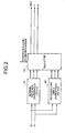
- Fig. 3 is a block diagram of a second example of the internal configuration of the receiver 8.
- the receiver 8 includes a selector 91, an absolute value output subtractor 92, a comparator 93, a determinator 94, and a receiver 95 for SE0.
- the selector 91 selects the threshold of 250 mV for Tiny J, for example, and when the threshold level changing signal is negated, it selects the threshold of 125 mV for normal operation, for example.
- the absolute value output subtractor 92 obtains an absolute value of a difference between the D+ signal voltage and the D- signal voltage, namely, the value of
- the comparator 93 compares the threshold selected by the selector 91 with the absolute value supplied from the absolute value output subtractor 92.
- the determinator 94 determines the J state or the K state based on the compared result from the comparator 93 and the sign supplied from the absolute value output subtractor 92. Specifically, when the absolute value is the thresholds or more and the sign is plus, the J signal is asserted and the K signal is negated (J state). When the sign is minus, the J signal is negated and the K signal is asserted (K state). On the other hand, when the absolute value is smaller than the thresholds, the signals are invalid. When both the D+ signal and the D- signal are smaller than, for example, 800 mV, the receiver 95 for SE0 asserts the SE0 signal (SE0 state), and when one of the signals is, for example, 800 mV or more, it negates the SE0 signal.
- the receiver 8 can have the following configuration.
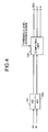
- Fig. 4 is a block diagram of a third example of the internal configuration of the receiver 8.
- the receiver 8 includes analog/digital (A/D) converters 101 and 102, and a computing unit 103.
- the A/D converter 101 converts the D+ signal into a digital signal.
- the A/D converter 102 converts the D- signal into a digital signal.
- the computing unit 103 asserts or negates the SE0 signal, the J signal, and the K signal according to the outputs (digital converted values) from the A/D converters 101 and 102, and the threshold level changing signal supplied from the reset control circuit 7.
- the computing unit 103 When both the digital converted value of the D+ signal and the digital converted value of the D- signal are smaller than, for example, 800 mV, the computing unit 103 asserts the SE0 signal (SE0 state). When one of the signals is, for example, 800 mV or more, the computing unit 103 negates the SE0 signal. When the digital converted value of the D+ signal is, for example, 150 mV or more, the computing unit 103 asserts the J signal (negates the K signal) so as to bring the USB bus into the J state. When the digital converted value of the D- signal is, for example, 150 mV or more, the computing unit 103 asserts the K signal (negates the J signal) so as to bring the USB bus into the K state. When both the digital converted value of the D+ signal and the digital converted value of the D- signal are smaller than, for example, 150 mV, the signals are invalid.
- Fig. 5 is a flowchart of the first example of the control at the time of handshaking.
- the SE0 timer 3 starts to count the duration of the SE0 state.
- the SE0 timer 3 asserts an SE03ms detected signal to the suspending/reset discriminating circuit 4.
- the suspending/reset discriminating circuit 4 closes the switch 5, and connects the pull-up resistor 6 to the D+ data line (step S502).
- the suspending/reset discriminating circuit 4 discriminates whether the USB bus is in the SE0 state (step S503). Accordingly, when the USB bus is in the SE0 state ("YES" at step S503), the suspending/reset discriminating circuit 4 recognizes the host to be in the reset state, and asserts the reset detected signal to the reset control circuit 7.
- the reset control circuit 7 asserts the threshold level changing signal to the receiver 8 for high-speed mode. Accordingly, the receiver 8 changes the threshold into, for example, 250 mV (step S504).
- a driver (not shown in Fig. 1 ) asserts the D- signal so as to execute chirp driving K (step S505). The driver negates the D- signal so as to end the chirp driving K, and maintains the SE0 state of the USB bus until the USB bus is brought into the J state or the K state (step S506).
- the reset control circuit 7 When the reset control circuit 7 detects that the USB bus is in the K state ("YES" at step S508), it negates the threshold level changing signal to the receiver 8. Accordingly, the receiver 8 for high-speed mode returns the threshold to, for example, 125 mV (step S509). In such a manner, the USB 2.0 compatible device recognizes its connecting destination to be an HS host (step S510), and the handshaking is ended so that the reset is ended.
- the reset control circuit 7 detects that the USB bus is brought into the J state ("YES" at step S507), it negates the threshold level changing signal to the receiver 8 for high-speed mode.
- the receiver 8 for high-speed mode returns the threshold to, for example, 125 mV (step S511).
- the USB 2.0 compatible device recognizes its connecting destination to be an FS host (step S512), and the handshaking is ended so that the reset is ended.
- the threshold of the receiver 8 for high-speed mode is returned to, for example, 125 mV (step S511) similarly to when the J state is detected. Accordingly, the USB 2.0 compatible device recognizes its connecting destination to be the FS host (step S512). The handshaking is ended, and the reset is ended.
- the suspending/reset discriminating circuit 4 recognizes the host to be in the suspended state (step S513), and the handshaking is ended.
- Fig. 6 is a flowchart of the second example of the control at the time of handshaking. As shown in Fig. 6 , when the handshaking during reset is started, steps S601 to S605 are executed sequentially. Steps S601, S602, S603, S604, and S605 are the same as steps S501, S502, S503, S504, and S505 in the first control example, and thus the redundant explanation is omitted.
- the reset control circuit 7 When the reset control circuit 7 detects a predetermined number of repetition times of the K state and the J state in the USB bus, for example, at least three times ("YES” at step S607) before predetermined time, for example, 2.5 ms elapses from the end of the chirp driving K with the USB bus being in the SE0 state ("NO” at step S606), the reset control circuit 7 negates the threshold level changing signal to the receiver 8 for high-speed mode. Accordingly, the receiver 8 for high-speed mode returns the threshold to, for example, 125 mV (step S608). In such a manner, the USB 2.0 compatible device recognizes its connecting destination to be the HS host (step S609), and the handshaking is ended so that the reset is ended.
- the USB 2.0 compatible device recognizes its connecting destination to be the FS host (step S610), the handshaking is ended, and the reset is ended.
- the suspending/reset discriminating circuit 4 recognizes the host to be in the suspended state (step S611), and the handshaking is ended.
- the threshold of the receiver 8 for high-speed mode is changed into a value higher than the voltage of the USB bus in the Tiny J state, for example, 250 mV at the time of the detection of reset. Accordingly, the detection can be properly made that the USB bus is in the K state according to the response from the USB host without detecting Tiny J.
- the HS host is not, therefore, misrecognized as the FS host and is properly recognized as the HS host, so that the USB device can be connected to the HS host in the high-speed mode.
- the present invention is not limited to the above embodiment and modifications can be made.
- the threshold of the receiver 8, the detecting time of the SE0 state and the like can be selected widely according to the standards of USB.
- the threshold of the receiver 8 after reset is not limited to 125 mV and can be a value within the standards of USB.
- the threshold of the receiver for high-speed mode is changed into a value higher than the voltage of the USB bus in Tiny J state at the time when the reset is detected. Accordingly, the detection can be made properly that the USB bus is in the K state according to the response from the USB host without detecting Tiny J.
- the HS host is not, therefore, misrecognized as the FS host and is properly recognized as the HS host, so that the USB device can be connected to the HS host in the high-speed mode.
- the present invention is suitable for providing the USB 2.0 compatible device that prevents the detection of Tiny J, properly recognizes a USB 2.0 incompatible HS host as the HS host, and is connected to the HS host in the high-speed mode. Further, the present invention is suitable for providing the control method for the USB 2.0 compatible device that prevents the detection of Tiny J, properly recognizes the USB 2.0 incompatible HS host as the HS host, and is connected to the HS host in the high-speed mode.
Landscapes
- Engineering & Computer Science (AREA)
- Theoretical Computer Science (AREA)
- General Engineering & Computer Science (AREA)
- Physics & Mathematics (AREA)
- General Physics & Mathematics (AREA)
- Computer Hardware Design (AREA)
- Information Transfer Systems (AREA)
Applications Claiming Priority (2)
| Application Number | Priority Date | Filing Date | Title |
|---|---|---|---|
| EP02793451A EP1580648A4 (de) | 2002-12-27 | 2002-12-27 | Usb-einrichtung und verfahren zur steuerung einer usb-einrichtung |
| PCT/JP2002/013820 WO2004061636A1 (ja) | 2002-12-27 | 2002-12-27 | Usb装置およびusb装置の制御方法 |
Related Parent Applications (1)
| Application Number | Title | Priority Date | Filing Date |
|---|---|---|---|
| EP02793451A Division EP1580648A4 (de) | 2002-12-27 | 2002-12-27 | Usb-einrichtung und verfahren zur steuerung einer usb-einrichtung |
Publications (2)
| Publication Number | Publication Date |
|---|---|
| EP1986103A2 true EP1986103A2 (de) | 2008-10-29 |
| EP1986103A3 EP1986103A3 (de) | 2008-12-03 |
Family
ID=32697334
Family Applications (2)
| Application Number | Title | Priority Date | Filing Date |
|---|---|---|---|
| EP02793451A Ceased EP1580648A4 (de) | 2002-12-27 | 2002-12-27 | Usb-einrichtung und verfahren zur steuerung einer usb-einrichtung |
| EP08154518A Withdrawn EP1986103A3 (de) | 2002-12-27 | 2002-12-27 | USB-Vorrichtung und Verfahren zur Steuerung der USB-Vorrichtung |
Family Applications Before (1)
| Application Number | Title | Priority Date | Filing Date |
|---|---|---|---|
| EP02793451A Ceased EP1580648A4 (de) | 2002-12-27 | 2002-12-27 | Usb-einrichtung und verfahren zur steuerung einer usb-einrichtung |
Country Status (6)
| Country | Link |
|---|---|
| US (1) | US8069287B2 (de) |
| EP (2) | EP1580648A4 (de) |
| JP (1) | JPWO2004061636A1 (de) |
| CN (1) | CN100561407C (de) |
| AU (1) | AU2002359942A1 (de) |
| WO (1) | WO2004061636A1 (de) |
Families Citing this family (22)
| Publication number | Priority date | Publication date | Assignee | Title |
|---|---|---|---|---|
| US7106517B2 (en) * | 2003-12-31 | 2006-09-12 | General Electric Company | Display optical films |
| US7281069B2 (en) | 2004-08-31 | 2007-10-09 | Broadcom Corporation | Method and system for extending the functionality of an embedded USB transceiver interface to handle threshold shift of a USB 2.0 bus during high-speed chirp |
| KR100822798B1 (ko) * | 2006-01-16 | 2008-04-17 | 삼성전자주식회사 | 유에스비 장치 및 유에스 장치를 포함하는 데이터 처리시스템 |
| JP4876236B2 (ja) * | 2006-09-01 | 2012-02-15 | 日本電産サンキョー株式会社 | Usb通信システム,usbデバイス,及びusb通信システムの異常検出方法 |
| JP2008152533A (ja) * | 2006-12-18 | 2008-07-03 | Hitachi Omron Terminal Solutions Corp | Usb機器及びusb接続システム及びusb機器の取り外し認識擬制方法及びusb機器の再認識方法 |
| TWI334545B (en) * | 2007-02-12 | 2010-12-11 | Via Tech Inc | A usb device and a mode detecting method thereof |
| CN103428003B (zh) | 2008-12-11 | 2017-03-01 | 美国莱迪思半导体公司 | 视频及音频数字互动接口的电力传输系统 |
| US8020049B2 (en) * | 2008-12-18 | 2011-09-13 | Avago Technologies Ecbu Ip (Singapore) Pte. Ltd. | Detection of and recovery from an electrical fast transient/burst (EFT/B) on a universal serial bus (USB) device |
| CN102835091B (zh) | 2010-01-12 | 2017-07-04 | 美国莱迪思半导体公司 | 多媒体USB数据传输透过数字视频和音频(DiiVA)的交互界面 |
| US8432981B1 (en) * | 2010-03-10 | 2013-04-30 | Smsc Holdings S.A.R.L. | High frequency and idle communication signal state detection |
| JP5587642B2 (ja) * | 2010-03-11 | 2014-09-10 | 株式会社メガチップス | 通信デバイスおよび通信システム |
| CN102541798B (zh) * | 2010-12-07 | 2015-06-10 | 瑞昱半导体股份有限公司 | 通用串行总线系统的在线校正方法及其装置 |
| CN102446143A (zh) * | 2011-09-26 | 2012-05-09 | 翔德电子科技(深圳)有限公司 | 照相机与ipad连接时避开USB识别的方法 |
| CN103810127B (zh) * | 2012-11-13 | 2017-09-08 | 深圳市中兴微电子技术有限公司 | Usb低速设备数据传输控制方法及控制器 |
| CN103995791B (zh) * | 2013-02-19 | 2016-12-28 | 群联电子股份有限公司 | 电子装置的信号传输电路及信号传输接口的检测方法 |
| US10387343B2 (en) * | 2015-04-07 | 2019-08-20 | International Business Machines Corporation | Processing of events for accelerators utilized for parallel processing |
| US10127162B2 (en) * | 2016-06-29 | 2018-11-13 | Intel Corporation | Efficient low cost on-die configurable bridge controller |
| US10908671B2 (en) | 2016-09-30 | 2021-02-02 | Maxim Integrated Products, Inc. | Method and apparatus for disabling high speed bus operation under high common mode voltage conditions |
| CN106776386B (zh) * | 2016-12-30 | 2019-12-03 | 维沃移动通信有限公司 | 一种识别外部usb设备的方法及移动终端 |
| FR3071938A1 (fr) * | 2017-10-02 | 2019-04-05 | Stmicroelectronics (Rousset) Sas | Detection d'une condition temporelle sur un bus bifilaire |
| JP2019175308A (ja) * | 2018-03-29 | 2019-10-10 | セイコーエプソン株式会社 | 回路装置、電子機器及びケーブルハーネス |
| CN112100104B (zh) * | 2020-08-05 | 2022-07-19 | 深圳市广和通无线股份有限公司 | 通用串行总线装置、系统及通讯设备 |
Family Cites Families (20)
| Publication number | Priority date | Publication date | Assignee | Title |
|---|---|---|---|---|
| JPS6210930A (ja) * | 1985-07-06 | 1987-01-19 | Nec Corp | スケルチ検出回路 |
| JPH0974427A (ja) * | 1995-09-04 | 1997-03-18 | Tokai Rika Co Ltd | 通信装置 |
| JP3610424B2 (ja) * | 1997-04-23 | 2005-01-12 | カシオ計算機株式会社 | 電子機器及びインタフェース回路 |
| JPH10301898A (ja) | 1997-04-23 | 1998-11-13 | Casio Comput Co Ltd | 電子機器及びインタフェース回路 |
| JP4400937B2 (ja) * | 1997-09-29 | 2010-01-20 | 株式会社ルネサステクノロジ | Usbデバイス |
| JPH11194993A (ja) * | 1998-01-06 | 1999-07-21 | Alps Electric Co Ltd | Usbコントローラ |
| JP3144374B2 (ja) * | 1998-02-06 | 2001-03-12 | 日本電気株式会社 | 信号変化加速バス駆動回路 |
| US6363085B1 (en) * | 1998-03-23 | 2002-03-26 | Multivideo Labs, Inc. | Universal serial bus repeater |
| JPH11305880A (ja) * | 1998-04-23 | 1999-11-05 | Sony Corp | Usb機器およびusbハブ装置 |
| US6457086B1 (en) * | 1999-11-16 | 2002-09-24 | Apple Computers, Inc. | Method and apparatus for accelerating detection of serial bus device speed signals |
| US6744810B1 (en) * | 1999-12-10 | 2004-06-01 | Intel Corporation | Signal repeater for voltage intolerant components used in a serial data line |
| EP1183611B1 (de) * | 1999-12-24 | 2007-03-14 | Koninklijke Philips Electronics N.V. | Emulation einer geräteabschaltung |
| US6559686B1 (en) * | 2000-05-12 | 2003-05-06 | Cypress Semiconductor Corp. | Analog envelope detector |
| JP2002312085A (ja) * | 2001-02-07 | 2002-10-25 | Nagano Fujitsu Component Kk | インターフェイス自動判別周辺機器 |
| KR100375234B1 (ko) * | 2001-03-30 | 2003-03-08 | 삼성전자주식회사 | 스퀄치 감지 회로 |
| TW512232B (en) * | 2001-05-08 | 2002-12-01 | Prolific Technology Inc | USB connection-detection circuitry and operation methods of the same |
| JP3651411B2 (ja) * | 2001-05-14 | 2005-05-25 | セイコーエプソン株式会社 | 信号受信回路、データ転送制御装置及び電子機器 |
| JP3651410B2 (ja) * | 2001-05-14 | 2005-05-25 | セイコーエプソン株式会社 | 送信回路、データ転送制御装置及び電子機器 |
| KR100421050B1 (ko) * | 2001-10-12 | 2004-03-04 | 삼성전자주식회사 | 범용직렬버스 호스트가 즉각적으로 리셋동작을 수행토록범용직렬버스의 신호 상태를 구현하는 로직 회로를구비하는 범용직렬버스 장치 |
| CN100463340C (zh) * | 2005-08-19 | 2009-02-18 | 鸿富锦精密工业(深圳)有限公司 | 通用串行总线接口功率控制电路 |
-
2002
- 2002-12-27 CN CNB028295234A patent/CN100561407C/zh not_active Expired - Fee Related
- 2002-12-27 AU AU2002359942A patent/AU2002359942A1/en not_active Abandoned
- 2002-12-27 EP EP02793451A patent/EP1580648A4/de not_active Ceased
- 2002-12-27 WO PCT/JP2002/013820 patent/WO2004061636A1/ja not_active Ceased
- 2002-12-27 JP JP2004544170A patent/JPWO2004061636A1/ja active Pending
- 2002-12-27 EP EP08154518A patent/EP1986103A3/de not_active Withdrawn
-
2005
- 2005-02-25 US US11/065,563 patent/US8069287B2/en not_active Expired - Fee Related
Non-Patent Citations (1)
| Title |
|---|
| JOHN GARNEY ET AL.: "USB Hardware & Software, Japanese version", 1999, INFOCREATE CO., LTD. |
Also Published As
| Publication number | Publication date |
|---|---|
| EP1580648A1 (de) | 2005-09-28 |
| AU2002359942A1 (en) | 2004-07-29 |
| WO2004061636A1 (ja) | 2004-07-22 |
| US20050144345A1 (en) | 2005-06-30 |
| US8069287B2 (en) | 2011-11-29 |
| CN100561407C (zh) | 2009-11-18 |
| JPWO2004061636A1 (ja) | 2006-05-18 |
| EP1580648A4 (de) | 2007-04-18 |
| CN1650249A (zh) | 2005-08-03 |
| EP1986103A3 (de) | 2008-12-03 |
Similar Documents
| Publication | Publication Date | Title |
|---|---|---|
| EP1986103A2 (de) | USB-Vorrichtung und Verfahren zur Steuerung der USB-Vorrichtung | |
| US6208924B1 (en) | Bus system for data transfer | |
| EP1950668B1 (de) | Zeitsteuerung von einem Zustandsübergang einer seriellen Datenleitung in einer I2C-Steuerung | |
| US5412644A (en) | Serial bus system with a single-wire line | |
| CN101004729A (zh) | Usb装置及具有该usb装置的数据处理系统 | |
| KR100910419B1 (ko) | 표시 장치의 전원 감시 제어 장치 | |
| US7552258B2 (en) | Method and system for extending the functionality of an embedded USB transceiver interface to handle threshold shift of a USB 2.0 bus during high-speed chirp | |
| EP4152700B1 (de) | Controller area network(can)-sende-empfänger | |
| EP1638007A2 (de) | Datenverarbeitungsvorrichtung, externe Speichervorrichtung, Datenverarbeitungssystem und Datenübertragungsverfahren | |
| US6922790B2 (en) | Three wire communication protocol | |
| US7944807B2 (en) | System and method for implementing a single-wire serial protocol | |
| CN116737642A (zh) | 一种spi主设备、中断方法及系统 | |
| JP2009175092A (ja) | 断線検出装置 | |
| JP2002312085A (ja) | インターフェイス自動判別周辺機器 | |
| CN1458591A (zh) | Usb/ps2接口自动识别装置及方法 | |
| JP2004145813A (ja) | 終端制御装置、およびユニバーサルシリアルバスシステム | |
| US12536121B1 (en) | Vol compliant I2C isolation scheme | |
| JP5587642B2 (ja) | 通信デバイスおよび通信システム | |
| JP2004005283A (ja) | Usbホスト/デバイス接続機構 | |
| JPH05336002A (ja) | インターフェース回路 | |
| JP2002183082A (ja) | シリアル通信装置 | |
| JPH02182058A (ja) | データ受信回路 | |
| JPH08328705A (ja) | パラレルインタフェース回路およびプリンタシステムおよびプリンタ装置 |
Legal Events
| Date | Code | Title | Description |
|---|---|---|---|
| PUAI | Public reference made under article 153(3) epc to a published international application that has entered the european phase |
Free format text: ORIGINAL CODE: 0009012 |
|
| AC | Divisional application: reference to earlier application |
Ref document number: 1580648 Country of ref document: EP Kind code of ref document: P |
|
| AK | Designated contracting states |
Kind code of ref document: A2 Designated state(s): DE FR GB |
|
| PUAL | Search report despatched |
Free format text: ORIGINAL CODE: 0009013 |
|
| AK | Designated contracting states |
Kind code of ref document: A3 Designated state(s): DE FR GB |
|
| RAP1 | Party data changed (applicant data changed or rights of an application transferred) |
Owner name: FUJITSU MICROELECTRONICS LIMITED |
|
| AKX | Designation fees paid | ||
| REG | Reference to a national code |
Ref country code: DE Ref legal event code: 8566 |
|
| STAA | Information on the status of an ep patent application or granted ep patent |
Free format text: STATUS: THE APPLICATION IS DEEMED TO BE WITHDRAWN |
|
| 18D | Application deemed to be withdrawn |
Effective date: 20090604 |