EP2058856A2 - Halbleitervorrichtung und Verfahren für ihre Montage - Google Patents
Halbleitervorrichtung und Verfahren für ihre Montage Download PDFInfo
- Publication number
- EP2058856A2 EP2058856A2 EP08168935A EP08168935A EP2058856A2 EP 2058856 A2 EP2058856 A2 EP 2058856A2 EP 08168935 A EP08168935 A EP 08168935A EP 08168935 A EP08168935 A EP 08168935A EP 2058856 A2 EP2058856 A2 EP 2058856A2
- Authority
- EP
- European Patent Office
- Prior art keywords
- lead terminals
- chip pad
- grooves
- semiconductor package
- package
- Prior art date
- Legal status (The legal status is an assumption and is not a legal conclusion. Google has not performed a legal analysis and makes no representation as to the accuracy of the status listed.)
- Withdrawn
Links
Images




Classifications
-
- H—ELECTRICITY
- H10—SEMICONDUCTOR DEVICES; ELECTRIC SOLID-STATE DEVICES NOT OTHERWISE PROVIDED FOR
- H10W—GENERIC PACKAGES, INTERCONNECTIONS, CONNECTORS OR OTHER CONSTRUCTIONAL DETAILS OF DEVICES COVERED BY CLASS H10
- H10W74/00—Encapsulations, e.g. protective coatings
- H10W74/10—Encapsulations, e.g. protective coatings characterised by their shape or disposition
- H10W74/111—Encapsulations, e.g. protective coatings characterised by their shape or disposition the semiconductor body being completely enclosed
-
- H—ELECTRICITY
- H10—SEMICONDUCTOR DEVICES; ELECTRIC SOLID-STATE DEVICES NOT OTHERWISE PROVIDED FOR
- H10W—GENERIC PACKAGES, INTERCONNECTIONS, CONNECTORS OR OTHER CONSTRUCTIONAL DETAILS OF DEVICES COVERED BY CLASS H10
- H10W76/00—Containers; Fillings or auxiliary members therefor; Seals
- H10W76/10—Containers or parts thereof
-
- H—ELECTRICITY
- H05—ELECTRIC TECHNIQUES NOT OTHERWISE PROVIDED FOR
- H05K—PRINTED CIRCUITS; CASINGS OR CONSTRUCTIONAL DETAILS OF ELECTRIC APPARATUS; MANUFACTURE OF ASSEMBLAGES OF ELECTRICAL COMPONENTS
- H05K3/00—Apparatus or processes for manufacturing printed circuits
- H05K3/30—Assembling printed circuits with electric components, e.g. with resistors
- H05K3/32—Assembling printed circuits with electric components, e.g. with resistors electrically connecting electric components or wires to printed circuits
- H05K3/34—Assembling printed circuits with electric components, e.g. with resistors electrically connecting electric components or wires to printed circuits by soldering
- H05K3/341—Surface mounted components
-
- H—ELECTRICITY
- H05—ELECTRIC TECHNIQUES NOT OTHERWISE PROVIDED FOR
- H05K—PRINTED CIRCUITS; CASINGS OR CONSTRUCTIONAL DETAILS OF ELECTRIC APPARATUS; MANUFACTURE OF ASSEMBLAGES OF ELECTRICAL COMPONENTS
- H05K3/00—Apparatus or processes for manufacturing printed circuits
- H05K3/30—Assembling printed circuits with electric components, e.g. with resistors
- H05K3/32—Assembling printed circuits with electric components, e.g. with resistors electrically connecting electric components or wires to printed circuits
- H05K3/34—Assembling printed circuits with electric components, e.g. with resistors electrically connecting electric components or wires to printed circuits by soldering
- H05K3/341—Surface mounted components
- H05K3/3431—Leadless components
- H05K3/3442—Leadless components having edge contacts, e.g. leadless chip capacitors, chip carriers
-
- H—ELECTRICITY
- H10—SEMICONDUCTOR DEVICES; ELECTRIC SOLID-STATE DEVICES NOT OTHERWISE PROVIDED FOR
- H10W—GENERIC PACKAGES, INTERCONNECTIONS, CONNECTORS OR OTHER CONSTRUCTIONAL DETAILS OF DEVICES COVERED BY CLASS H10
- H10W70/00—Package substrates; Interposers; Redistribution layers [RDL]
- H10W70/40—Leadframes
- H10W70/411—Chip-supporting parts, e.g. die pads
-
- H—ELECTRICITY
- H10—SEMICONDUCTOR DEVICES; ELECTRIC SOLID-STATE DEVICES NOT OTHERWISE PROVIDED FOR
- H10W—GENERIC PACKAGES, INTERCONNECTIONS, CONNECTORS OR OTHER CONSTRUCTIONAL DETAILS OF DEVICES COVERED BY CLASS H10
- H10W70/00—Package substrates; Interposers; Redistribution layers [RDL]
- H10W70/40—Leadframes
- H10W70/421—Shapes or dispositions
- H10W70/424—Cross-sectional shapes
-
- H—ELECTRICITY
- H10—SEMICONDUCTOR DEVICES; ELECTRIC SOLID-STATE DEVICES NOT OTHERWISE PROVIDED FOR
- H10W—GENERIC PACKAGES, INTERCONNECTIONS, CONNECTORS OR OTHER CONSTRUCTIONAL DETAILS OF DEVICES COVERED BY CLASS H10
- H10W70/00—Package substrates; Interposers; Redistribution layers [RDL]
- H10W70/40—Leadframes
- H10W70/456—Materials
- H10W70/457—Materials of metallic layers on leadframes
-
- H—ELECTRICITY
- H05—ELECTRIC TECHNIQUES NOT OTHERWISE PROVIDED FOR
- H05K—PRINTED CIRCUITS; CASINGS OR CONSTRUCTIONAL DETAILS OF ELECTRIC APPARATUS; MANUFACTURE OF ASSEMBLAGES OF ELECTRICAL COMPONENTS
- H05K2201/00—Indexing scheme relating to printed circuits covered by H05K1/00
- H05K2201/03—Conductive materials
- H05K2201/0332—Structure of the conductor
- H05K2201/0364—Conductor shape
- H05K2201/0373—Conductors having a fine structure, e.g. providing a plurality of contact points with a structured tool
-
- H—ELECTRICITY
- H05—ELECTRIC TECHNIQUES NOT OTHERWISE PROVIDED FOR
- H05K—PRINTED CIRCUITS; CASINGS OR CONSTRUCTIONAL DETAILS OF ELECTRIC APPARATUS; MANUFACTURE OF ASSEMBLAGES OF ELECTRICAL COMPONENTS
- H05K2201/00—Indexing scheme relating to printed circuits covered by H05K1/00
- H05K2201/10—Details of components or other objects attached to or integrated in a printed circuit board
- H05K2201/10613—Details of electrical connections of non-printed components, e.g. special leads
- H05K2201/10742—Details of leads
- H05K2201/10886—Other details
- H05K2201/10931—Exposed leads, i.e. encapsulation of component partly removed for exposing a part of lead, e.g. for soldering purposes
-
- H—ELECTRICITY
- H10—SEMICONDUCTOR DEVICES; ELECTRIC SOLID-STATE DEVICES NOT OTHERWISE PROVIDED FOR
- H10W—GENERIC PACKAGES, INTERCONNECTIONS, CONNECTORS OR OTHER CONSTRUCTIONAL DETAILS OF DEVICES COVERED BY CLASS H10
- H10W72/00—Interconnections or connectors in packages
- H10W72/071—Connecting or disconnecting
- H10W72/075—Connecting or disconnecting of bond wires
-
- H—ELECTRICITY
- H10—SEMICONDUCTOR DEVICES; ELECTRIC SOLID-STATE DEVICES NOT OTHERWISE PROVIDED FOR
- H10W—GENERIC PACKAGES, INTERCONNECTIONS, CONNECTORS OR OTHER CONSTRUCTIONAL DETAILS OF DEVICES COVERED BY CLASS H10
- H10W72/00—Interconnections or connectors in packages
- H10W72/50—Bond wires
- H10W72/531—Shapes of wire connectors
- H10W72/5366—Shapes of wire connectors the bond wires having kinks
-
- H—ELECTRICITY
- H10—SEMICONDUCTOR DEVICES; ELECTRIC SOLID-STATE DEVICES NOT OTHERWISE PROVIDED FOR
- H10W—GENERIC PACKAGES, INTERCONNECTIONS, CONNECTORS OR OTHER CONSTRUCTIONAL DETAILS OF DEVICES COVERED BY CLASS H10
- H10W72/00—Interconnections or connectors in packages
- H10W72/50—Bond wires
- H10W72/541—Dispositions of bond wires
- H10W72/5449—Dispositions of bond wires not being orthogonal to a side surface of the chip, e.g. fan-out arrangements
-
- H—ELECTRICITY
- H10—SEMICONDUCTOR DEVICES; ELECTRIC SOLID-STATE DEVICES NOT OTHERWISE PROVIDED FOR
- H10W—GENERIC PACKAGES, INTERCONNECTIONS, CONNECTORS OR OTHER CONSTRUCTIONAL DETAILS OF DEVICES COVERED BY CLASS H10
- H10W72/00—Interconnections or connectors in packages
- H10W72/90—Bond pads, in general
- H10W72/931—Shapes of bond pads
- H10W72/932—Plan-view shape, i.e. in top view
-
- H—ELECTRICITY
- H10—SEMICONDUCTOR DEVICES; ELECTRIC SOLID-STATE DEVICES NOT OTHERWISE PROVIDED FOR
- H10W—GENERIC PACKAGES, INTERCONNECTIONS, CONNECTORS OR OTHER CONSTRUCTIONAL DETAILS OF DEVICES COVERED BY CLASS H10
- H10W72/00—Interconnections or connectors in packages
- H10W72/90—Bond pads, in general
- H10W72/951—Materials of bond pads
-
- H—ELECTRICITY
- H10—SEMICONDUCTOR DEVICES; ELECTRIC SOLID-STATE DEVICES NOT OTHERWISE PROVIDED FOR
- H10W—GENERIC PACKAGES, INTERCONNECTIONS, CONNECTORS OR OTHER CONSTRUCTIONAL DETAILS OF DEVICES COVERED BY CLASS H10
- H10W72/00—Interconnections or connectors in packages
- H10W72/90—Bond pads, in general
- H10W72/951—Materials of bond pads
- H10W72/952—Materials of bond pads comprising metals or metalloids, e.g. PbSn, Ag or Cu
-
- H—ELECTRICITY
- H10—SEMICONDUCTOR DEVICES; ELECTRIC SOLID-STATE DEVICES NOT OTHERWISE PROVIDED FOR
- H10W—GENERIC PACKAGES, INTERCONNECTIONS, CONNECTORS OR OTHER CONSTRUCTIONAL DETAILS OF DEVICES COVERED BY CLASS H10
- H10W74/00—Encapsulations, e.g. protective coatings
-
- H—ELECTRICITY
- H10—SEMICONDUCTOR DEVICES; ELECTRIC SOLID-STATE DEVICES NOT OTHERWISE PROVIDED FOR
- H10W—GENERIC PACKAGES, INTERCONNECTIONS, CONNECTORS OR OTHER CONSTRUCTIONAL DETAILS OF DEVICES COVERED BY CLASS H10
- H10W90/00—Package configurations
- H10W90/701—Package configurations characterised by the relative positions of pads or connectors relative to package parts
- H10W90/751—Package configurations characterised by the relative positions of pads or connectors relative to package parts of bond wires
- H10W90/756—Package configurations characterised by the relative positions of pads or connectors relative to package parts of bond wires between a chip and a stacked lead frame, conducting package substrate or heat sink
-
- Y—GENERAL TAGGING OF NEW TECHNOLOGICAL DEVELOPMENTS; GENERAL TAGGING OF CROSS-SECTIONAL TECHNOLOGIES SPANNING OVER SEVERAL SECTIONS OF THE IPC; TECHNICAL SUBJECTS COVERED BY FORMER USPC CROSS-REFERENCE ART COLLECTIONS [XRACs] AND DIGESTS
- Y02—TECHNOLOGIES OR APPLICATIONS FOR MITIGATION OR ADAPTATION AGAINST CLIMATE CHANGE
- Y02P—CLIMATE CHANGE MITIGATION TECHNOLOGIES IN THE PRODUCTION OR PROCESSING OF GOODS
- Y02P70/00—Climate change mitigation technologies in the production process for final industrial or consumer products
- Y02P70/50—Manufacturing or production processes characterised by the final manufactured product
Definitions
- the present invention relates to a semiconductor package and mounting method for improving reliability by strengthening adhesion strength between a printed circuit board and a surface mounting package.
- Commonly used surface mounting packages include a small outline J-Iead (SOJ) type surface mounting package, and a special usage Zigzag Inline Package (ZIP) surface mounting package. Further, there is a Thin Small Outline Package (TSOP) type of surface mounting package that is suitable for a standardized memory card.
- SOJ small outline J-Iead
- ZIP Zigzag Inline Package
- TSOP Thin Small Outline Package
- a typical surface mounting package is formed with gold-plated nickel, and configured with a chip pad on which a semiconductor device will be adhered, and lead terminals for electrically connecting the package to an external device. Since the semiconductor device and the lead terminals include either an adhesive tape or an adhesive agent, they are electrically connected with wires. Further, the package is completed by forming an enveloping unit that is molded with epoxy molding compound (EMC) in order to protect the semiconductor device from any damage due to external thermal effects and external mechanical or chemical impacts.
- EMC epoxy molding compound
- a semiconductor package has a chip pad on which a semiconductor device is disposed, and has lead terminals, wherein at least one of the chip pad and the lead terminals comprise a plurality of grooves.
- the semiconductor device may be connected to the lead terminals by wiring.
- the chip pad may be made of nickel coated with gold.
- the grooves may extend in one direction.
- the grooves may have a mesh shape. According to an aspect of the present invention, the grooves have a matrix shape. According to an aspect of the present invention, the grooves are formed when the chip pad and the lead terminals are formed, or after the semiconductor package is completed.
- a method includes providing a printed circuit board having terminals; coating cream solder on the terminals of the printed circuit board; disposing a semiconductor package having a chip pad and lead terminals on the printed circuit board, the chip pad and the lead terminals having a plurality of grooves; forcing the cream solder into the plurality of grooves by pressing together the semiconductor package and the printed circuit board; and adhering the semiconductor package onto the printed circuit board by hardening the cream solder.
- a semiconductor package includes: a semiconductor device, a chip pad on which the semiconductor device is disposed; lead terminals electrically connected to the semiconductor device by respective wires; and an enveloping unit that is molded to envelop the semiconductor device, the chip pad, and the lead terminals, except for a surface of each of the chip pad and the lead terminals that are externally exposed, wherein the chip pad and the lead terminals comprise a plurality of grooves that are formed over the exposed surfaces of the chip pad and the lead terminals.
- a mounting method of a semiconductor package includes: providing a printed circuit board having terminals; coating cream solder on the terminals of the printed circuit board; disposing a semiconductor package on the printed circuit board, the semiconductor package includes: a semiconductor device, a chip pad on which the semiconductor device is disposed, lead terminals electrically connected to the semiconductor device by respective wires, and an enveloping unit that is molded to envelop the semiconductor device, the chip pad, and the lead terminals, except for a surface of each of the chip pad and the lead terminals that are externally exposed, wherein the chip pad and the lead terminals comprise a plurality of grooves that are formed over the exposed surfaces of the chip pad and the lead terminals, and the chip pad and the lead terminals are aligned to the terminals of the printed circuit board; forcing the cream solder into the plurality of grooves by pressing together the semiconductor package and the printed circuit board; and adhering the semiconductor package onto the printed circuit board by hardening the cream solder.
- FIG. 1A is a plan view illustrating a structure of a semiconductor package according to an aspect of the present invention
- FIG. 1B is a side elevational view of the semiconductor package of FIG. 1A .
- a package 100 may comprise a chip pad 110 on which a semiconductor device 120 is disposed, a plurality of lead terminals 130 to externally connect the semiconductor device 120, and wires 140 to electrically connect the semiconductor device 120 to the lead terminals 130.
- the semiconductor device 120 and the lead terminals 130 are electrically connected to each other by fixing with either an adhesive tape or an adhesive agent. Further, the package is completed by forming an enveloping unit 150 that is molded with an epoxy molding compound (EMC) in order to protect the semiconductor device 120 from any damage due to thermal effects, or external mechanical or chemical impacts.
- EMC epoxy molding compound
- the enveloping unit 150 may be formed to entirely envelop the semiconductor device 120, and most of the chip pad 110 on which the semiconductor device 120 is disposed and most of the plurality of lead terminals 130, except for one surface on each of the chip pad 110 and the plurality of lead terminals 130.
- the non-enveloped surfaces of the chip pad 110 and the plurality of lead terminals 130 are substantially coplanar, and are externally exposed.
- a plurality of grooves 160 may be formed on a surface of both the chip pad 110 on which the semiconductor device is disposed, and the lead terminals 130, respectively, in order to improve shearing strength thereof by acquiring increased adhesive (or surface) areas available for adhesion.
- the grooves 160 may be extendedly formed in one direction as illustrated in FIG. 1C , in a mesh shape as illustrated in FIG. 1D , or in a matrix shape as illustrated in FIG. 1E .
- the surfaces on which the plurality of grooves 160 are formed are substantially coplanar.
- shapes or cross sectional profiles of the grooves 160 may be formed as desired. That is, edges of the grooves 160 may be formed as one of right angles (as shown in FIG. 1B ) and curved surfaces. In aspects of the present invention, other shapes of the grooves 160 are also possible, such as triangular or pyramidal shapes.
- cross sectional shapes of the grooves 160 may outline a square wave pattern as shown in FIG. 1B , or may outline a triangular wave, a sinusoidal wave, or other wave patterns.
- the periodicity of the grooves 160 may be regular so that intervals between each groove 160 may be equal, though such is not required. Accordingly, the grooves 160 may also be formed at irregular intervals or at any desired intervals.
- FIG. 1D illustrates a mesh shape arrangement of the grooves 160
- FIG. 1E illustrates a matrix shape arrangement of the grooves 160. That is, FIG. 1D illustrates an arrangement of a set of the grooves 160 that extend perpendicularly to another set of the grooves 160
- FIG. 1E illustrates an arrangement of grooves 160 that extend discontinuously.
- square shaped land areas are formed in between the grooves 160 in FIG. 1D
- square shaped indentations are formed by the grooves 160 in FIG. 1E , such is not required, and the shapes of the lands or indentations that may be formed by the grooves 160 may be circular, hexagonal, triangular, or other shapes.
- the grooves 160 may be formed on at least one of the chip pad 110 and the lead terminals 130 (i.e., on the chip pad 110, the lead terminals 130, or both). Also, the grooves 160 may be formed when the chip pad 110 and the lead terminals 130 are formed, or after the package 100 is completed once an epoxy molding compound (EMC) is molded thereon, for example.
- EMC epoxy molding compound
- a cream solder is filled up in the grooves 160. Accordingly, areas of adhesion may be widened or increased so that shearing strength of the chip pad 110 and/or the lead terminals 130 relative to a printed circuit board may be improved, and greater solder joint reliability can be acquired therefore.
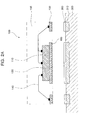
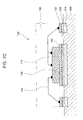
- FIGS. 2A through 2D are drawings illustrating a mounting method of a semiconductor package according to aspects of the present invention.
- FIG. 2A shows cream solder 200 that is coated on PCB terminals 310 formed on the printed circuit board (PCB) 300 before adhering the printed circuit board 300 to the package 100.
- PCB printed circuit board
- the package 100 may comprise the chip pad 110 and the lead terminals 130.
- the chip pad 110 and the lead terminals 130 may have a plurality of the grooves 160 at surfaces to which the printed circuit board 300 is adhered.
- the chip pad 110 and the lead terminals 130 are adhered to the printed circuit board 300 by way of the PCB terminals 310.
- FIG. 2B shows disposing the package 100 on the printed circuit board 300 in order to adhere the package 100 to the printed circuit board 300.
- the chip pad 110 and lead terminals 130 may be disposed on the PCB terminals 310 and cream solder 200, respectively, while being closely contacted.
- FIG. 2C shows adhering the package 100 to the printed circuit board 300.
- the cream solder 200 may flow into the grooves 160 formed on the chip pad 110 and the lead terminals 130 of the package 100 by melting the cream solder 200 by use of heat, and pressing the package 100 and the printed circuit board 300 together.
- FIG. 2D shows incorporating the package 100 into the printed circuit board 300.
- some of the melted cream solder 200 may flow into the grooves 160 of both the chip pad 110 and the lead terminals 130, and harden, thereby mounting the package 100 to the printed circuit board 300.
- filling up or intrusion of the cream solder 200 into the grooves 160 enable interlocking of the land portions of the chip pad 110 and/or the lead terminals 130 with the cream solder 200 once the cream solder 200 is hardened, to increase shear strength of the package 100 relative to the printed circuit board 300.
- the adhesive areas may be widened or increased so that the shearing strength may be improved and greater solder joint reliability can be acquired.
- At least one of refers to alternatives chosen from available elements so as to include one or more of the elements.
- the elements available include elements X, Y, and Z
Landscapes
- Engineering & Computer Science (AREA)
- Manufacturing & Machinery (AREA)
- Microelectronics & Electronic Packaging (AREA)
- Electric Connection Of Electric Components To Printed Circuits (AREA)
- Structures Or Materials For Encapsulating Or Coating Semiconductor Devices Or Solid State Devices (AREA)
- Lead Frames For Integrated Circuits (AREA)
Applications Claiming Priority (1)
| Application Number | Priority Date | Filing Date | Title |
|---|---|---|---|
| KR1020070114898A KR100984132B1 (ko) | 2007-11-12 | 2007-11-12 | 반도체 패키지 및 그 실장방법 |
Publications (2)
| Publication Number | Publication Date |
|---|---|
| EP2058856A2 true EP2058856A2 (de) | 2009-05-13 |
| EP2058856A3 EP2058856A3 (de) | 2014-08-27 |
Family
ID=40122504
Family Applications (1)
| Application Number | Title | Priority Date | Filing Date |
|---|---|---|---|
| EP08168935.8A Withdrawn EP2058856A3 (de) | 2007-11-12 | 2008-11-12 | Halbleitervorrichtung und Verfahren für ihre Montage |
Country Status (5)
| Country | Link |
|---|---|
| US (1) | US8319319B2 (de) |
| EP (1) | EP2058856A3 (de) |
| JP (1) | JP2009124095A (de) |
| KR (1) | KR100984132B1 (de) |
| CN (1) | CN101436575B (de) |
Families Citing this family (21)
| Publication number | Priority date | Publication date | Assignee | Title |
|---|---|---|---|---|
| US8357998B2 (en) * | 2009-02-09 | 2013-01-22 | Advanced Semiconductor Engineering, Inc. | Wirebonded semiconductor package |
| EP2337068A1 (de) * | 2009-12-18 | 2011-06-22 | Nxp B.V. | Im Voraus gelötete leitungslose Kapselung |
| US9418919B2 (en) | 2010-07-29 | 2016-08-16 | Nxp B.V. | Leadless chip carrier having improved mountability |
| US8766100B2 (en) | 2011-03-02 | 2014-07-01 | Samsung Electronics Co., Ltd. | Printed circuit board and semiconductor package using the same |
| KR101237668B1 (ko) * | 2011-08-10 | 2013-02-26 | 삼성전기주식회사 | 반도체 패키지 기판 |
| US9373609B2 (en) * | 2012-10-18 | 2016-06-21 | Infineon Technologies Ag | Bump package and methods of formation thereof |
| KR101423136B1 (ko) * | 2012-12-28 | 2014-07-25 | 한국광기술원 | 반도체 본딩 조립체 및 반도체 본딩 조립 방법 |
| US20140239428A1 (en) * | 2013-02-28 | 2014-08-28 | Infineon Technologies Ag | Chip arrangement and a method for manufacturing a chip arrangement |
| CN104659010B (zh) * | 2015-02-11 | 2018-03-16 | 江苏长电科技股份有限公司 | 一种四方扁平无引脚型态封装的引线框结构与封装体结构 |
| KR20180044725A (ko) * | 2016-10-24 | 2018-05-03 | 주식회사 엘지화학 | 전류 측정을 위한 션트 저항기 |
| CN106714451A (zh) * | 2016-12-19 | 2017-05-24 | 长沙牧泰莱电路技术有限公司 | 一种复合式印刷电路板及其制作方法 |
| CN108987557A (zh) * | 2018-07-04 | 2018-12-11 | 佛山市国星半导体技术有限公司 | 一种倒装led芯片及其制作方法、led器件 |
| DE102018130936B4 (de) * | 2018-12-05 | 2022-08-11 | Infineon Technologies Ag | Halbleitergehäuse, Metallblech zur Anwendung in einem Halbleitergehäuse und Verfahren zum Herstellen eines Halbleitergehäuses |
| CN112435975B (zh) * | 2019-02-22 | 2022-07-19 | 西安航思半导体有限公司 | 散热dfn半导体器件封装结构 |
| CN113451228B (zh) * | 2019-03-06 | 2022-07-19 | 西安航思半导体有限公司 | 高强度qfn封装结构 |
| CN109904125B (zh) * | 2019-03-06 | 2021-02-19 | 西安航思半导体有限公司 | 耐高温qfn封装结构的制备方法 |
| KR102512688B1 (ko) * | 2019-12-05 | 2023-03-23 | 한국전자기술연구원 | 소자접합성능향상방법 |
| CN113015324B (zh) * | 2019-12-19 | 2023-05-09 | 华为技术有限公司 | 电路板组件、电子设备、加工电路板组件的方法 |
| CN118039583A (zh) * | 2022-11-03 | 2024-05-14 | 三赢科技(深圳)有限公司 | 封装模组 |
| CN222532136U (zh) * | 2024-04-29 | 2025-02-25 | 深圳市洲明科技股份有限公司 | Led灯珠与显示屏 |
| CN119277635B (zh) * | 2024-10-16 | 2025-10-17 | 深圳市宏灏精密线路有限公司 | 一种复合型印刷电路板及其制作方法 |
Family Cites Families (26)
| Publication number | Priority date | Publication date | Assignee | Title |
|---|---|---|---|---|
| US5069626A (en) | 1987-07-01 | 1991-12-03 | Western Digital Corporation | Plated plastic castellated interconnect for electrical components |
| JPH0217854U (de) * | 1988-07-18 | 1990-02-06 | ||
| FR2636453B1 (fr) * | 1988-09-14 | 1992-01-17 | Sgs Thomson Microelectronics | Procede d'encapsulation de circuits-integres notamment pour cartes a puces |
| JPH05102381A (ja) * | 1991-10-09 | 1993-04-23 | Mitsubishi Electric Corp | 半導体装置 |
| JPH0577947U (ja) * | 1992-03-27 | 1993-10-22 | 安藤電気株式会社 | 表面実装用icのl字形端子 |
| JP3597913B2 (ja) * | 1995-07-20 | 2004-12-08 | 松下電器産業株式会社 | 半導体装置とその実装方法 |
| KR19980048268A (ko) | 1996-12-17 | 1998-09-15 | 김광호 | 홈이 형성된 외부 리드를 갖는 반도체 칩 패키지 및 그가 실장되는 구조 |
| JP2912308B2 (ja) * | 1997-11-14 | 1999-06-28 | 静岡日本電気株式会社 | 表面実装部品の半田付け構造 |
| US6365976B1 (en) * | 1999-02-25 | 2002-04-02 | Texas Instruments Incorporated | Integrated circuit device with depressions for receiving solder balls and method of fabrication |
| KR100960739B1 (ko) * | 1999-02-26 | 2010-06-01 | 텍사스 인스트루먼츠 인코포레이티드 | 열적으로 향상된 반도체 볼 그리드 어레이 디바이스 및 그제조 방법 |
| JP2000294719A (ja) * | 1999-04-09 | 2000-10-20 | Hitachi Ltd | リードフレームおよびそれを用いた半導体装置ならびにその製造方法 |
| KR20010004529A (ko) | 1999-06-29 | 2001-01-15 | 김영환 | 웨이퍼 레벨 패키지 및 그의 제조 방법 |
| JP4034073B2 (ja) * | 2001-05-11 | 2008-01-16 | 株式会社ルネサステクノロジ | 半導体装置の製造方法 |
| US20030006055A1 (en) * | 2001-07-05 | 2003-01-09 | Walsin Advanced Electronics Ltd | Semiconductor package for fixed surface mounting |
| JP4243270B2 (ja) | 2001-12-14 | 2009-03-25 | 株式会社ルネサステクノロジ | 半導体装置の製造方法 |
| JP2003188335A (ja) | 2001-12-14 | 2003-07-04 | Hitachi Ltd | 半導体装置及びその製造方法 |
| JP2004039882A (ja) | 2002-07-04 | 2004-02-05 | Tateyama Kagaku Kogyo Kk | チップ型サーミスタとその製造方法 |
| US6777788B1 (en) * | 2002-09-10 | 2004-08-17 | National Semiconductor Corporation | Method and structure for applying thick solder layer onto die attach pad |
| AU2002357592A1 (en) * | 2002-12-18 | 2004-07-09 | K-Tech Devices Corp. | Flip-chip mounting electronic component and method for producing the same, circuit board and method for producing the same, method for producing package |
| US8330258B2 (en) * | 2003-12-24 | 2012-12-11 | Stmicroelectronics, Inc. | System and method for improving solder joint reliability in an integrated circuit package |
| JP2006100753A (ja) | 2004-09-30 | 2006-04-13 | Sanyo Electric Co Ltd | 半導体モジュールおよびその製造方法 |
| JP4111199B2 (ja) * | 2005-03-10 | 2008-07-02 | ヤマハ株式会社 | 半導体パッケージ、及びこれを回路基板に実装する方法 |
| JP4860939B2 (ja) * | 2005-04-08 | 2012-01-25 | ローム株式会社 | 半導体装置 |
| JP2006319030A (ja) | 2005-05-11 | 2006-11-24 | Matsushita Electric Ind Co Ltd | 回路基板とその製造方法、および半導体装置とその製造方法 |
| US7405106B2 (en) * | 2006-05-23 | 2008-07-29 | International Business Machines Corporation | Quad flat no-lead chip carrier with stand-off |
| JP2006237653A (ja) | 2006-06-12 | 2006-09-07 | Kyocera Chemical Corp | 半導体装置の接着方法とそれに使用される接着剤 |
-
2007
- 2007-11-12 KR KR1020070114898A patent/KR100984132B1/ko not_active Expired - Fee Related
-
2008
- 2008-02-28 JP JP2008048152A patent/JP2009124095A/ja active Pending
- 2008-09-23 US US12/235,739 patent/US8319319B2/en not_active Expired - Fee Related
- 2008-11-12 CN CN2008101740332A patent/CN101436575B/zh not_active Expired - Fee Related
- 2008-11-12 EP EP08168935.8A patent/EP2058856A3/de not_active Withdrawn
Also Published As
| Publication number | Publication date |
|---|---|
| US20090121362A1 (en) | 2009-05-14 |
| JP2009124095A (ja) | 2009-06-04 |
| CN101436575A (zh) | 2009-05-20 |
| KR100984132B1 (ko) | 2010-09-28 |
| EP2058856A3 (de) | 2014-08-27 |
| US8319319B2 (en) | 2012-11-27 |
| KR20090048833A (ko) | 2009-05-15 |
| CN101436575B (zh) | 2010-10-13 |
Similar Documents
| Publication | Publication Date | Title |
|---|---|---|
| US8319319B2 (en) | Semiconductor package and mounting method thereof | |
| US12094725B2 (en) | Leadframe package with pre-applied filler material | |
| US5018005A (en) | Thin, molded, surface mount electronic device | |
| US5053357A (en) | Method of aligning and mounting an electronic device on a printed circuit board using a flexible substrate having fixed lead arrays thereon | |
| US8659146B2 (en) | Lead frame based, over-molded semiconductor package with integrated through hole technology (THT) heat spreader pin(s) and associated method of manufacturing | |
| US9013030B2 (en) | Leadframe, semiconductor package including a leadframe and method for producing a leadframe | |
| US9711343B1 (en) | Molded leadframe substrate semiconductor package | |
| US4054938A (en) | Combined semiconductor device and printed circuit board assembly | |
| US6965159B1 (en) | Reinforced lead-frame assembly for interconnecting circuits within a circuit module | |
| CN101432868A (zh) | 用于使用牺牲金属基础的封装类型的三维封装方案 | |
| CA2119325C (en) | Molded plastic packaging of electronic devices | |
| US9847283B1 (en) | Semiconductor device with wettable corner leads | |
| US5559305A (en) | Semiconductor package having adjacently arranged semiconductor chips | |
| JPH02260450A (ja) | 半導体装置およびその実装方法 | |
| JP3366062B2 (ja) | オーバモールド形半導体装置及びその製造方法 | |
| US20060258058A1 (en) | Surface-mounted device with leads | |
| JP3680398B2 (ja) | プリント配線板 | |
| US7563649B1 (en) | Chip packaging with metal frame pin grid array | |
| JP4679991B2 (ja) | 半導体装置 | |
| US7750450B2 (en) | Stacked die package with stud spacers | |
| JP2000277677A (ja) | リードフレーム、半導体パッケージ及びその製造方法 | |
| KR19980047800A (ko) | 이층 리드 구조를 갖는 고방열 반도체 패키지 및 그의 제조 방법 | |
| US20110177629A1 (en) | Chip Packaging with Metal Frame Pin Grid Array | |
| JPH11251481A (ja) | 半導体装置用セラミックパッケージおよび半導体装置 | |
| JPH07106496A (ja) | 半導体装置 |
Legal Events
| Date | Code | Title | Description |
|---|---|---|---|
| PUAI | Public reference made under article 153(3) epc to a published international application that has entered the european phase |
Free format text: ORIGINAL CODE: 0009012 |
|
| 17P | Request for examination filed |
Effective date: 20081112 |
|
| AK | Designated contracting states |
Kind code of ref document: A2 Designated state(s): AT BE BG CH CY CZ DE DK EE ES FI FR GB GR HR HU IE IS IT LI LT LU LV MC MT NL NO PL PT RO SE SI SK TR |
|
| AX | Request for extension of the european patent |
Extension state: AL BA MK RS |
|
| RAP1 | Party data changed (applicant data changed or rights of an application transferred) |
Owner name: SAMSUNG SDI CO., LTD. |
|
| PUAL | Search report despatched |
Free format text: ORIGINAL CODE: 0009013 |
|
| AK | Designated contracting states |
Kind code of ref document: A3 Designated state(s): AT BE BG CH CY CZ DE DK EE ES FI FR GB GR HR HU IE IS IT LI LT LU LV MC MT NL NO PL PT RO SE SI SK TR |
|
| AX | Request for extension of the european patent |
Extension state: AL BA MK RS |
|
| RIC1 | Information provided on ipc code assigned before grant |
Ipc: H01L 23/00 20060101ALI20140723BHEP Ipc: H01L 23/31 20060101AFI20140723BHEP Ipc: H01L 23/495 20060101ALI20140723BHEP Ipc: H05K 3/34 20060101ALI20140723BHEP |
|
| AKX | Designation fees paid |
Designated state(s): DE FR GB HU |
|
| AXX | Extension fees paid |
Extension state: MK Extension state: RS Extension state: AL Extension state: BA |
|
| STAA | Information on the status of an ep patent application or granted ep patent |
Free format text: STATUS: THE APPLICATION HAS BEEN WITHDRAWN |
|
| 18W | Application withdrawn |
Effective date: 20160616 |