EP2172976A2 - Dispositif semi-conducteur - Google Patents
Dispositif semi-conducteur Download PDFInfo
- Publication number
- EP2172976A2 EP2172976A2 EP09167598A EP09167598A EP2172976A2 EP 2172976 A2 EP2172976 A2 EP 2172976A2 EP 09167598 A EP09167598 A EP 09167598A EP 09167598 A EP09167598 A EP 09167598A EP 2172976 A2 EP2172976 A2 EP 2172976A2
- Authority
- EP
- European Patent Office
- Prior art keywords
- layer
- region
- depletion
- lifetime
- layer forming
- Prior art date
- Legal status (The legal status is an assumption and is not a legal conclusion. Google has not performed a legal analysis and makes no representation as to the accuracy of the status listed.)
- Withdrawn
Links
Images




Classifications
-
- H—ELECTRICITY
- H10—SEMICONDUCTOR DEVICES; ELECTRIC SOLID-STATE DEVICES NOT OTHERWISE PROVIDED FOR
- H10D—INORGANIC ELECTRIC SEMICONDUCTOR DEVICES
- H10D18/00—Thyristors
- H10D18/60—Gate-turn-off devices
-
- H—ELECTRICITY
- H10—SEMICONDUCTOR DEVICES; ELECTRIC SOLID-STATE DEVICES NOT OTHERWISE PROVIDED FOR
- H10D—INORGANIC ELECTRIC SEMICONDUCTOR DEVICES
- H10D62/00—Semiconductor bodies, or regions thereof, of devices having potential barriers
- H10D62/10—Shapes, relative sizes or dispositions of the regions of the semiconductor bodies; Shapes of the semiconductor bodies
- H10D62/17—Semiconductor regions connected to electrodes not carrying current to be rectified, amplified or switched, e.g. channel regions
- H10D62/192—Base regions of thyristors
- H10D62/199—Anode base regions of thyristors
Definitions
- the present invention relates to a semiconductor device with four-layer structure (PNPN structure) such as thyristor.
- PNPN structure four-layer structure
- GCT element gate commutation thyristor element
- Fig. 6 is a diagram showing a basic circuit applicable to a GCT element in the case that a snubber circuit is added.
- Fig. 7 is a diagram showing a basic circuit applicable to a GCT element in the case that any snubber circuit is not added.
- reference numeral 101 is a GCT element that is connected in series to a power source and to a circuit where a load and a free wheel diode are connected in parallel.
- Numeral 102 is a snubber circuit, comprising a capacitor, a diode and a resistor, which is connected between the anode and the cathode of the GCT element 101.
- Fig. 6 is a diagram showing a basic circuit applicable to a GCT element in the case that a snubber circuit is added.
- Fig. 7 is a diagram showing a basic circuit applicable to a GCT element in the case that any snubber circuit is not added.
- reference numeral 101 is a
- numeral 103 is a voltage clamping circuit, comprising a diode and a capacitor, which is connected between the anode and the cathode of the GCT element 101.
- Numeral 104 is a resistor connected between the power source and a terminal located between the diode and the capacitor in the voltage clamping circuit 103.
- the remaining elements in Fig. 7 are the same as Fig. 6 , except the snubber circuit 102. Therefore, a further description is omitted herein.
- the GCT element 101 begins to restore its voltage blocking characteristic, and begins to block the voltage. Simultaneously, a current begins to flow in the snubber circuit 102 that is connected in parallel with the GCT element 101. In this manner, it is possible to cause the current that has been flowing in the GCT element 101 to flow in the snubber circuit 102 and to reduce the current in the GCT element 101. As a result, a turn-off operation with a small amount of turn-off loss can be performed.
- the GCT element 101 begins to restore its voltage blocking characteristic, and begins to block the voltage. Then, the element voltage reaches a source voltage, and upon reaching the source voltage, the current flowing in the GCT element 101 begins to reduce. This means that the current continues to flow in the element until the element voltage reaches the source voltage, and turn-off loss of the GCT element itself increases by several tens of percent or more as compared with the case where the snubber circuit 102 is added.
- Fig. 8 is a sectional view showing a conventional GCT element.
- Fig. 9 is a top view showing the conventional GCT element viewed from a cathode side.
- Fig. 8 shows a section taken along the line A-A in Fig. 9 .
- numeral 111 is an N - region made of an N - semiconductor substrate containing impurities of a lower-concentration.
- the N - region 111 is comprised of two layers; one is a first layer 111a formed to be short in lifetime due to lattice defect therein, and the other is a second layer 111b formed to be locally close to an N region 112 in the N - region 111 and to be shorter in lifetime than the first layer 111a.
- Numeral 112 is the N region made of an N-type semiconductor formed on the face of the second layer 111b side in the N - region 111.
- Numeral 113 is a circular-shaped or torus-shape P emitter region made of a P-type semiconductor, formed selectively on top of the N region 112.
- Numeral 114 is a P base region made of a P-type semiconductor formed on the face of the first layer 111a side in the N - region 111.
- Numeral 115 is an N emitter region made of an N-type semiconductor, formed selectively on top of the P base region 114.
- Numeral 116 is a cathode electrode made of a metal such as aluminum, formed on top of the N emitter region 115.
- Numeral 117 is a gate electrode formed on top of such areas of the P base region 114 where the N emitter region 115 is not formed.
- Numeral 118 is an anode electrode formed on top of the P emitter region 113 and also on top of the N region 112 that are estranged by the P emitter region 113. The P emitter region 113 and the N region 112 are short-circuited at the anode electrode 118 and form an anode short-circuit structure.
- FIG. 9 A top view from a cathode side of the element is shown in Fig. 9 .
- the gate electrode 117 is formed on top of the P base region 114.
- four elliptical regions are formed selectively in the areas where the electrode 117 is not formed.
- the N emitter region 115 is formed so as not to be in contact with the gate electrode 117, and the elliptical cathode electrode 116 is formed on top of the N emitter region 115.
- Fig.10 shows a distribution of lifetimes of the semiconductors in the N - region 111 shown in Figs. 8 and 9 .
- lattice defects are evenly formed in the N - region 111 by electron beam irradiation technique to shorten the lifetime.
- comparatively heavy ions such as proton are implanted into the second layer 111b to produce a regional crystal imperfection in the area making consequently the lifetime of the second layer 111b shorter than that of the first layer 111a (i.e., the N - region 111 excluding the second layer 111b).
- the lifetime of the first layer 111a in the N - region 111 is controlled to be within a range of 50 to 200 ⁇ s and that of the second layer 111b is controlled to be within a range of 1 to 100 ⁇ s, respectively.
- the semiconductor device indicated in both Fig. 8 and Fig. 9 is arranged to be connected to the circuit without any snubber circuit, as shown in Fig. 7 .
- a depletion layer starts to be formed in a direction from the PN junction between the P base region 114 and the N - region 111 toward the anode side. Since the lifetime of the first layer 111a of the N - region 111 is formed shorter, the depletion layer is quickly formed in the area near the PN junction between the P base region 114 and the N - region 111. Then, this depletion layer extends to the anode side and reaches the second layer 111b in the N - region 111.
- Fig. 11 shows a main electric current and a main electric voltage at a turn-off operation of the conventional semiconductor device.
- Fig. 11 shows a main electric current and a main electric voltage at a turn-off operation of the conventional semiconductor device.
- extension speed of a depletion layer increases, and current dropping speed is increased. Consequently, with the increase of current dropping speed, a very high spike voltage is generated.
- a further semiconductor device is disclosed in the Japanese Patent Publication (unexamined) No. 235782/87 .
- this semiconductor device an additional regional layer of a short lifetime is formed in the vicinity of a cathode electrode side in an N - region of the semiconductor device.
- the lifetime of the N - region is evenly shortened by means of electron beam irradiation technique so that the depletion layer is quickly formed at the turn-off operation.
- the current dropping speed increases and the spike voltage is bound to become very high.
- the present invention was made to resolve the above-discussed problems and has an object of providing a semiconductor devices capable of controlling spike voltage at the turn-off operation.
- a semiconductor device comprises a first region composed of a first conductor, a second region composed of a second conductor formed on top of the first region, a third region composed of the first conductor formed on top of the second region and a fourth region composed of the second conductor formed on top of the third region, the second region being comprised of a depletion-layer forming auxiliary layer having a short lifetime formed in the vicinity of the third region, a tail-current suppression layer having a shorter lifetime than that of the depletion-layer forming auxiliary layer and formed in the vicinity of the first region and a depletion-layer forming suppression layer having a longer lifetime than that of the depletion-layer forming auxiliary layer and formed between the depletion-layer forming auxiliary layer and the tail-current suppression layer.
- the depletion-layer forming suppression layer is formed in such a manner that lifetime on the third region side is shorter than that on the first region side. In this case, in the depletion-layer forming suppression layer, extension of the depletion layer is suppressed in due order, and a value of spike voltage can be kept small.
- the depletion-layer forming suppression layer is formed in such a manner that lifetime becomes longer consecutively in due order in a direction from the third region side to the first region side. In this case, extension of the depletion layer can be slackened little by little and a spike voltage can be suppressed all the more.
- the lifetime of the depletion-layer forming suppression layer is in the range of 200 to 500 ⁇ s.
- thickness ratio of the depletion-layer forming suppression layer is in the range of 15 to 40 percent of the second region.
- the tail-current suppression layer can be wider, and after the spike voltage is generated, a tail current can be quickly suppressed.
- thickness ratio of the depletion-layer forming suppression layer is in the range of 40 to 65 percent of the second region. In this case, the depletion-layer forming suppression layer can be wider, and the spike voltage can be further suppressed.
- a depletion-layer forming promotion layer having a lifetime shorter than that on the second region side of the depletion-layer forming auxiliary layers is formed on the third region side of the depletion-layer forming auxiliary layer.
- formation speed of the depletion layer can be further increased, and di/dt (current dropping speed) at an initial stage of turn-off can be prevented from lowering.
- a peak-voltage suppression layer is formed between the tail-current suppression layer in the second region and the first region in order to suppress formation speed of a depletion layer and to suppress a peak voltage generated at a turn-off operation of the semiconductor device.
- extension speed of the depletion layer being formed fast in the tail-current suppression layer can be suppressed again, whereby a peak voltage of the main voltage can be suppressed.
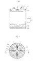
- Fig. 1 shows a sectional view showing a semiconductor device according to mode 1 of the invention.
- Fig. 2 is a top view, seen from a cathode side, of the semiconductor device according to mode 1 of the invention. More specifically, Fig. 1 is a sectional view taken along the line A-A shown in Fig. 2 .
- reference numeral 1 is an N - region serving as a second region made of an N-type semiconductor substrate such as silicon and containing impurities of a low concentration.
- the N - region is comprised of six layers whose lifetimes differ from one another and that are formed in such an order from an anode side as a first layer 1a, a second layer 1b, a third layer 1c, a fourth layer 1d, a fifth layer 1e and a sixth layer 1f.
- the third layer 1c and the fourth layer 1d form a depletion-layer forming suppression layer to suppress a spike voltage.
- These layers are formed to suppress formation speed of a depletion layer so that the spike voltage generated at the turn-off operation of the semiconductor device may be suppressed.
- the fifth layer 1e is formed to have a shorter lifetime than those of the depletion-layer forming suppression layer (the third layer 1c and the fourth layer 1d) in order to promote formation of the depletion-layer in its own area.
- the sixth layer 1f is a depletion-layer forming promotion layer, and is formed to have a shorter lifetime than that of the fifth layer 1e in order to promote formation of the depletion-layer further.
- both fifth layer 1e and sixth layer 1f form a depletion-layer forming auxiliary layer.
- the second layer 1b is a tail-current suppression layer formed in the vicinity of an N region 2 in order to suppress a tail current
- the first layer 1a is a peak-voltage suppression layer formed adjacent to the N region 2 in order to suppress peak current.
- each layer in the N - region 1 is formed to have a following percentage: 5% for the first layer 1a, 10% for the second layer 1b, 25% for the third layer 1c, 25% for the fourth layer 1d, 30% for the fifth layer 1e and 5% for the sixth layer 1f. Percentage of each layer, however, is not limited to the percentages mentioned above, but is variable according to characteristics of elements such as lifetime.
- each layer falls within the following range: 10 to 40 ⁇ m for the first layer 1a, 40 to 60 ⁇ m for the second layer 1b, 100 to 200 ⁇ m for the third layer 1c, 100 to 200 ⁇ m for the fourth layer 1d, 150 to 250 ⁇ m for the fifth layer 1e and 10 to 40 ⁇ m for the sixth layer 1f. It is preferable that thickness of the third layer 1c and the fourth layer 1d, serving as the depletion-layer forming suppression layer, occupies in the range of 40 to 60% of the N - region 1.
- Numeral 2 is the N region containing impurities of a higher concentration than that in the N - region 1, and formed on one side of the N - region 1.
- Numeral 3 is a P emitter region of a P-type semiconductor serving as a first region, and formed selectively on the opposite side of the N - region 1, in the N region 2.
- Numeral 4 is a P base region of the P-type semiconductor serving as a third region, and formed on the other side of the N - region 1.
- the numeral 5 is an N emitter region of an N-type semiconductor serving as a fourth region, and formed selectively on top of the P base region 4.
- Numeral 6 is a cathode electrode made of metal or other materials formed on top of the N emitter region 5.
- Numeral 7 is a gate electrode formed to surround the N emitter region 5 on top of the P base region 4 where the N emitter region 5 is not formed.
- Numeral 8 is an anode electrode formed on top of the P emitter region 3 and also on top of the N region 2 of an estrangement region between the P emitter regions 3. The P emitter region 3 and the N region 2 are short-circuited at the anode electrode 8 and form an anode short-circuit structure.
- the gate electrode 7 is formed on top of the P base region 4.
- four elliptical regions are formed selectively.
- the electrode 7 is not formed in the four elliptical regions.
- the N emitter region 5 placed without being in contact with the gate electrode 7 is formed, and the elliptical cathode electrode 6 is formed on top of the N emitter region 5.
- the four elliptical regions are formed in the areas, where the gate electrode 7 is not formed, selectively in a radial pattern from the center of the gate electrode 7, the structure is not limited to such an arrangement. It is preferable that plural elliptical region are formed in the same radial line otherwise in the opposite radial line.
- Fig. 3 is a diagram showing lifetime distribution of each layer of the N - region 1 in the semiconductor device shown in Fig. 1 and Fig. 2 .
- lifetime of the first layer 1a is formed to be the longest among the layers in the N - region 1 and to be in the range of 300 to 800 ⁇ s.
- extension of the depletion layer formed in the first layer 1a can be suppressed at the turn-off operation, whereby the peak voltage can be suppressed.
- Lifetime of the second layer 1b is formed to be the shortest among the layers in the N - region 1 and to be in the range of 1 to 100 ⁇ s. As a result, extension of the depletion layer formed in the second layer 1b is promoted at the turn-off operation and the tail current generated at the turn-off operation can be suppressed to be low.
- Each lifetime of the third layer 1c and the fourth layer 1d is formed to be longer than that of the fifth layer 1e, At the same time, lifetime of the third layer 1c and the fourth layer 1d are formed to be longer increasingly in order from the fourth layer 1d to the third layer 1c so that extension speed of the depletion layer formed in the layers may be suppressed.
- the lifetimes of the third layer 1c and the fourth layer 1d are respectively formed to be in the range of 200 to 500 ⁇ s and 100 to 300 ⁇ s.
- Lifetime of the fifth layer 1e is formed shorter than that of the fourth layer 1d so that a depletion layer may extend quickly at the turn-off operation.
- Lifetime of the sixth layer 1f is formed shorter than that of the fifth layer 1e so that a depletion layer may be formed quickly and that di/dt (current dropping speed) at the initial stage of turn-off can be prevented from lowering.
- the lifetimes of the fifth layer 1e and the sixth layer 1f are respectively formed to be in a range of 50 to 200 ⁇ s and 10 to 150 ⁇ s.
- ions such as proton are irradiated from the anode side before the anode electrode 8 is formed.
- the ions stop at a certain range determined by accelerated energy. It is certain that a very small amount of crystal defects are formed also in the region where the ions have passed through, but a larger amount of crystal defects are increasingly formed as comes closer to the range. In other words, a considerable amount of crystal defects are partially formed in the area where the ions stop, whereby it is possible to make lifetime short partially in that region.
- crystal-defects formation method in which ions can be irradiated onto a specific range for a specific layer, the above-mentioned lifetime distribution can be formed in an desired manner.
- a depletion layer can be consecutively formed.
- each layer is caused to increase or decrease consecutively, this arrangement is not restrictive. It is also preferable that increase or decrease takes place stepwise. Alternatively, a partial but sequential increase or decrease is also preferable.
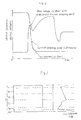
- Fig. 4 shows a main electric current and a main electric voltage in a turn-off operation of the semiconductor device shown in Fig. 1 and Fig. 2 .
- the depletion layer that starts being formed extends to the fourth layer 1d through the fifth layer 1e. Since the lifetime of the fifth layer 1e is formed comparatively short so that the depletion layer can easily extend, the depletion layer quickly extends until it reaches the fourth layer 1d. At this time, the main voltage recovers in proportion to the extension of the depletion layer, and then the element voltage comes to reach the source voltage. When the element voltage becomes higher, the extension of the depletion layer reaches the fourth layer 1d and the third layer 1c that have longer lifetimes.
- the depletion layer extends to the second layer 1b and the first layer 1a. Since the second layer 1b is formed to have the shortest lifetime in the N - region, extension speed of the depletion layer can be increased after the spike voltage arises, then, a tail current can be suppressed low. Furthermore, as the lifetime of the first layer 1a is made to be the longest in the N - region 1, extension of the depletion layer can be suppressed again so that a peak voltage of the main electric voltage can be suppressed.
- the lifetimes of the third layer and the fourth layer, serving as the depletion-layer forming suppression layer are formed longer than that of the fifth layer that is formed between the third and fourth layers and the P base region. Therefore, the value of the spike voltage at the turn-off operation can be suppressed low. Consequently, not only the turn-off loss can be reduced but also a highly controllable current can be applied.
- the lifetimes in the depletion-layer forming suppression layer are formed to be longer consecutively in an order from the cathode side to the anode side. Therefore, extension of the depletion layer can be gradually slackened and the spike voltage can be suppressed further.
- the sixth layer serving as the depletion-layer forming promotion layer whose lifetime is shorter than that of the fifth layer, is formedbetween the fifth layer and the P base region. Therefore, formation of the depletion-layer can be accelerated, di/dt (current dropping speed) at the initial stage of turn-off can be prevented form lowering, and the time for the element voltage to reaches the source voltage can be shortened further. As a result, the turn-off loss can be reduced all the more.
- the second layer serving as the tail-current suppression layer whose lifetime is the shortest, is formed between the third layer and the N region. Therefore, extension speed of the depletion layer, that is once slackened, can be increased and the tail current can be suppressed.
- the peak-voltage suppression layer is formed to suppress the peak voltage, between the third layer serving as the tail-current suppression layer and the N region. Therefore, extension speed of the depletion layer, once increased in the tail-current suppression layer, can be suppressed again and the peak voltage value of the main electric voltage can be suppressed.
- a semiconductor device according to mode 2 of the invention is a modification of the semiconductor device according to the foregoing mode 1 and is different in the aspect of lifetime distribution in the N - region of the semiconductor device shown in Fig. 1 and Fig. 2 .
- Fig. 5 shows lifetime distribution in an N - region of the semiconductor device according to mode 2 of the invention. Lifetimes of layers are the same as those in the foregoing mode 1 shown in Fig.3 , except a third layer 1c, and a further description is omitted herein. As shown in Fig.5 , lifetime of the third layer 1c is formed longer than that of a second layer 1b but shorter than that of a fourth layer 1d so that extension speed of a depletion layer formed in this layer is increased. The lifetime of the third layer 1c in this mode 2 is formed to be in the range of 50 to 200 ⁇ s. It is preferable that thickness ratio of the fourth layer 1d serving as a depletion-layer forming suppression layer, is in the range of 15 to 40% of the N - region.
- the lifetime distribution shown in Fig. 3 shows that the depletion-layer forming suppression layer continues up to the third layer 1c, and the lifetime becomes sharply shorter in the second layer 1b from that in the third layer 1c.
- the lifetime distribution shown in Fig. 5 shows that only the fourth layer 1d serves as the depletion-layer forming suppression layer, and extension speed of the depletion layer is gradually increased over the long range from the fourth layer 1d to the second layer 1b. Consequently, a tail current can be suppressed further.
- the lifetime of the fourth layer serving as the depletion-layer forming suppression layer is longer than that of a fifth layer formed between the fourth layer and a P base region. Therefore, value of the spike voltage generated at the turn-off operation can be suppressed low, and not only a highly controllable current is made applicable but also turn-off loss can be made smaller.
- the semiconductor device according to the present invention is applicable to a semiconductor device for a large amount of electric power such as GCT element dealing with a high pressure and a large amount of current without any snubber circuit.
Landscapes
- Thyristors (AREA)
Applications Claiming Priority (2)
| Application Number | Priority Date | Filing Date | Title |
|---|---|---|---|
| EP98941794.4A EP1039547B1 (fr) | 1998-09-10 | 1998-09-10 | Dispositif semi-conducteur |
| PCT/JP1998/004058 WO2000016406A1 (fr) | 1998-09-10 | 1998-09-10 | Dispositif semi-conducteur |
Related Parent Applications (2)
| Application Number | Title | Priority Date | Filing Date |
|---|---|---|---|
| EP98941794.4A Division-Into EP1039547B1 (fr) | 1998-09-10 | 1998-09-10 | Dispositif semi-conducteur |
| EP98941794.4 Division | 1998-09-10 |
Publications (2)
| Publication Number | Publication Date |
|---|---|
| EP2172976A2 true EP2172976A2 (fr) | 2010-04-07 |
| EP2172976A3 EP2172976A3 (fr) | 2010-05-05 |
Family
ID=14208954
Family Applications (2)
| Application Number | Title | Priority Date | Filing Date |
|---|---|---|---|
| EP09167598A Withdrawn EP2172976A3 (fr) | 1998-09-10 | 1998-09-10 | Dispositif semi-conducteur |
| EP98941794.4A Expired - Lifetime EP1039547B1 (fr) | 1998-09-10 | 1998-09-10 | Dispositif semi-conducteur |
Family Applications After (1)
| Application Number | Title | Priority Date | Filing Date |
|---|---|---|---|
| EP98941794.4A Expired - Lifetime EP1039547B1 (fr) | 1998-09-10 | 1998-09-10 | Dispositif semi-conducteur |
Country Status (4)
| Country | Link |
|---|---|
| US (1) | US6472692B1 (fr) |
| EP (2) | EP2172976A3 (fr) |
| JP (1) | JP3571353B2 (fr) |
| WO (1) | WO2000016406A1 (fr) |
Families Citing this family (11)
| Publication number | Priority date | Publication date | Assignee | Title |
|---|---|---|---|---|
| DE502007003501D1 (de) * | 2006-01-20 | 2010-06-02 | Infineon Technologies Austria | Nden halbleiterwafers und halbleiterbauelement |
| DE102006017487A1 (de) * | 2006-04-13 | 2007-10-18 | Fraunhofer-Gesellschaft zur Förderung der angewandten Forschung e.V. | Integriertes Beschaltungsbauelement auf Halbleiterbasis zur Schaltentlastung, Spannungsbegrenzung bzw. Schwingungsdämpfung |
| CN101754859B (zh) * | 2007-06-14 | 2012-05-30 | 麻省理工学院 | 用于沉积膜的方法和设备 |
| US9195004B2 (en) * | 2008-01-04 | 2015-11-24 | Massachusetts Institute Of Technology | Method and apparatus for forming structures of polymer nanobeads |
| US8383202B2 (en) * | 2008-06-13 | 2013-02-26 | Kateeva, Inc. | Method and apparatus for load-locked printing |
| WO2010017441A2 (fr) * | 2008-08-07 | 2010-02-11 | Massachusetts Institute Of Technology | Procédé et appareil de traçage de motifs latéral et vertical simultanément sur des pellicules organiques moléculaires |
| US8748219B2 (en) * | 2008-09-08 | 2014-06-10 | Massachusetts Institute Of Technology | Method and apparatus for super radiant laser action in half wavelength thick organic semiconductor microcavities |
| US20100188457A1 (en) * | 2009-01-05 | 2010-07-29 | Madigan Connor F | Method and apparatus for controlling the temperature of an electrically-heated discharge nozzle |
| EP2425470A2 (fr) * | 2009-05-01 | 2012-03-07 | Kateeva, Inc. | Procédé et appareil pour l'impression par condensation de vapeurs organiques |
| JP5972881B2 (ja) * | 2010-09-29 | 2016-08-17 | アーベーベー・テヒノロギー・アーゲー | 逆導通パワー半導体デバイス |
| JP6895094B2 (ja) * | 2017-12-28 | 2021-06-30 | 株式会社村田製作所 | 半導体装置 |
Citations (1)
| Publication number | Priority date | Publication date | Assignee | Title |
|---|---|---|---|---|
| JPS62235782A (ja) | 1986-04-07 | 1987-10-15 | Toyota Central Res & Dev Lab Inc | 半導体装置 |
Family Cites Families (14)
| Publication number | Priority date | Publication date | Assignee | Title |
|---|---|---|---|---|
| JPS4821198B1 (fr) * | 1968-08-15 | 1973-06-27 | ||
| JPS5821342A (ja) * | 1981-07-31 | 1983-02-08 | Hitachi Ltd | 半導体装置 |
| JPS649658A (en) | 1987-07-01 | 1989-01-12 | Mitsubishi Electric Corp | Gto thyristor |
| US6100575A (en) * | 1987-08-19 | 2000-08-08 | Mitsubishi Denki Kabushiki Kaisha | Semiconductor switching device having different carrier lifetimes between a first portion serving as a main current path and the remaining portion of the device |
| JPH0650738B2 (ja) * | 1990-01-11 | 1994-06-29 | 株式会社東芝 | 半導体装置及びその製造方法 |
| US5381026A (en) * | 1990-09-17 | 1995-01-10 | Kabushiki Kaisha Toshiba | Insulated-gate thyristor |
| JP3281145B2 (ja) * | 1993-10-28 | 2002-05-13 | 株式会社東芝 | Gtoサイリスタ |
| JPH07326732A (ja) * | 1994-06-02 | 1995-12-12 | Fuji Electric Co Ltd | 逆導通gtoサイリスタおよびその製造方法 |
| JPH08102545A (ja) * | 1994-09-30 | 1996-04-16 | Meidensha Corp | 半導体素子のライフタイム制御方法 |
| US5883403A (en) * | 1995-10-03 | 1999-03-16 | Hitachi, Ltd. | Power semiconductor device |
| JP3394383B2 (ja) * | 1996-03-18 | 2003-04-07 | 三菱電機株式会社 | サイリスタの製造方法およびサイリスタ |
| JPH1074959A (ja) * | 1996-07-03 | 1998-03-17 | Toshiba Corp | 電力用半導体素子 |
| WO1999007020A1 (fr) * | 1997-07-30 | 1999-02-11 | Siemens Aktiengesellschaft | Thyristor a commande par gachette |
| US6274892B1 (en) * | 1998-03-09 | 2001-08-14 | Intersil Americas Inc. | Devices formable by low temperature direct bonding |
-
1998
- 1998-09-10 WO PCT/JP1998/004058 patent/WO2000016406A1/fr not_active Ceased
- 1998-09-10 EP EP09167598A patent/EP2172976A3/fr not_active Withdrawn
- 1998-09-10 EP EP98941794.4A patent/EP1039547B1/fr not_active Expired - Lifetime
- 1998-09-10 JP JP55392799A patent/JP3571353B2/ja not_active Expired - Lifetime
-
2000
- 2000-05-09 US US09/566,737 patent/US6472692B1/en not_active Expired - Lifetime
Patent Citations (1)
| Publication number | Priority date | Publication date | Assignee | Title |
|---|---|---|---|---|
| JPS62235782A (ja) | 1986-04-07 | 1987-10-15 | Toyota Central Res & Dev Lab Inc | 半導体装置 |
Also Published As
| Publication number | Publication date |
|---|---|
| JP3571353B2 (ja) | 2004-09-29 |
| EP1039547B1 (fr) | 2016-03-23 |
| EP1039547A1 (fr) | 2000-09-27 |
| WO2000016406A1 (fr) | 2000-03-23 |
| EP2172976A3 (fr) | 2010-05-05 |
| EP1039547A4 (fr) | 2007-06-20 |
| US6472692B1 (en) | 2002-10-29 |
Similar Documents
| Publication | Publication Date | Title |
|---|---|---|
| US8163630B2 (en) | Method of manufacturing a semiconductor device | |
| US8829519B2 (en) | Semiconductor device | |
| JP2000323488A (ja) | ダイオードおよびその製造方法 | |
| US7557386B2 (en) | Reverse conducting IGBT with vertical carrier lifetime adjustment | |
| EP2172976A2 (fr) | Dispositif semi-conducteur | |
| JP6621925B2 (ja) | 半導体装置及びその製造方法 | |
| US11721755B2 (en) | Methods of forming semiconductor power devices having graded lateral doping | |
| US5466951A (en) | Controllable power semiconductor element with buffer zone and method for the manufacture thereof | |
| JP2706120B2 (ja) | Gtoパワーサイリスタ | |
| JP2004247593A (ja) | 半導体装置及びその製造方法 | |
| JP2001196606A (ja) | ダイオード | |
| JPWO2000016406A1 (ja) | 半導体装置 | |
| EP1713128B1 (fr) | IGBT et appareil de conversion de puissance électrique l'utilisant | |
| EP1780799B9 (fr) | Diode | |
| EP0862220A1 (fr) | Dispositif de commutation semiconducteur et convertisseur de puissance utilisant ledit dispositif et méthode de commande | |
| US4623910A (en) | Semiconductor device | |
| EP0977271B1 (fr) | Module IGBT semi-conducteur | |
| CN119170655A (zh) | 一种肖特基二极管及其制造方法 | |
| US7705369B2 (en) | High-voltage diode with optimized turn-off method and corresponding optimization method | |
| JPH10116998A (ja) | 半導体装置およびその製造方法 | |
| JP5077508B2 (ja) | 半導体装置およびその製造方法 | |
| JP2002016265A (ja) | 高耐圧ダイオード | |
| JPH07202226A (ja) | 電力半導体素子 | |
| JP7795077B2 (ja) | 半導体装置および電力変換装置 | |
| JP3962120B2 (ja) | ゲートターンオフサイリスタ |
Legal Events
| Date | Code | Title | Description |
|---|---|---|---|
| PUAI | Public reference made under article 153(3) epc to a published international application that has entered the european phase |
Free format text: ORIGINAL CODE: 0009012 |
|
| PUAL | Search report despatched |
Free format text: ORIGINAL CODE: 0009013 |
|
| AC | Divisional application: reference to earlier application |
Ref document number: 1039547 Country of ref document: EP Kind code of ref document: P |
|
| AK | Designated contracting states |
Kind code of ref document: A2 Designated state(s): CH DE LI |
|
| AK | Designated contracting states |
Kind code of ref document: A3 Designated state(s): CH DE LI |
|
| 17P | Request for examination filed |
Effective date: 20101104 |
|
| 17Q | First examination report despatched |
Effective date: 20130326 |
|
| STAA | Information on the status of an ep patent application or granted ep patent |
Free format text: STATUS: THE APPLICATION HAS BEEN WITHDRAWN |
|
| 18W | Application withdrawn |
Effective date: 20160414 |