EP2242341B1 - Verfahren zur herstellung einer struktur mit einem metallfilm, vorlagenmatrize zur verwendung in diesem verfahren und in dem verfahren hergestellte struktur - Google Patents
Verfahren zur herstellung einer struktur mit einem metallfilm, vorlagenmatrize zur verwendung in diesem verfahren und in dem verfahren hergestellte struktur Download PDFInfo
- Publication number
- EP2242341B1 EP2242341B1 EP09708441.2A EP09708441A EP2242341B1 EP 2242341 B1 EP2242341 B1 EP 2242341B1 EP 09708441 A EP09708441 A EP 09708441A EP 2242341 B1 EP2242341 B1 EP 2242341B1
- Authority
- EP
- European Patent Office
- Prior art keywords
- metal film
- film
- metal
- base
- concave
- Prior art date
- Legal status (The legal status is an assumption and is not a legal conclusion. Google has not performed a legal analysis and makes no representation as to the accuracy of the status listed.)
- Not-in-force
Links
Images








Classifications
-
- H—ELECTRICITY
- H05—ELECTRIC TECHNIQUES NOT OTHERWISE PROVIDED FOR
- H05K—PRINTED CIRCUITS; CASINGS OR CONSTRUCTIONAL DETAILS OF ELECTRIC APPARATUS; MANUFACTURE OF ASSEMBLAGES OF ELECTRICAL COMPONENTS
- H05K3/00—Apparatus or processes for manufacturing printed circuits
- H05K3/10—Apparatus or processes for manufacturing printed circuits in which conductive material is applied to the insulating support in such a manner as to form the desired conductive pattern
- H05K3/20—Apparatus or processes for manufacturing printed circuits in which conductive material is applied to the insulating support in such a manner as to form the desired conductive pattern by affixing prefabricated conductor pattern
- H05K3/205—Apparatus or processes for manufacturing printed circuits in which conductive material is applied to the insulating support in such a manner as to form the desired conductive pattern by affixing prefabricated conductor pattern using a pattern electroplated or electroformed on a metallic carrier
-
- C—CHEMISTRY; METALLURGY
- C23—COATING METALLIC MATERIAL; COATING MATERIAL WITH METALLIC MATERIAL; CHEMICAL SURFACE TREATMENT; DIFFUSION TREATMENT OF METALLIC MATERIAL; COATING BY VACUUM EVAPORATION, BY SPUTTERING, BY ION IMPLANTATION OR BY CHEMICAL VAPOUR DEPOSITION, IN GENERAL; INHIBITING CORROSION OF METALLIC MATERIAL OR INCRUSTATION IN GENERAL
- C23C—COATING METALLIC MATERIAL; COATING MATERIAL WITH METALLIC MATERIAL; SURFACE TREATMENT OF METALLIC MATERIAL BY DIFFUSION INTO THE SURFACE, BY CHEMICAL CONVERSION OR SUBSTITUTION; COATING BY VACUUM EVAPORATION, BY SPUTTERING, BY ION IMPLANTATION OR BY CHEMICAL VAPOUR DEPOSITION, IN GENERAL
- C23C14/00—Coating by vacuum evaporation, by sputtering or by ion implantation of the coating forming material
- C23C14/0005—Separation of the coating from the substrate
-
- C—CHEMISTRY; METALLURGY
- C23—COATING METALLIC MATERIAL; COATING MATERIAL WITH METALLIC MATERIAL; CHEMICAL SURFACE TREATMENT; DIFFUSION TREATMENT OF METALLIC MATERIAL; COATING BY VACUUM EVAPORATION, BY SPUTTERING, BY ION IMPLANTATION OR BY CHEMICAL VAPOUR DEPOSITION, IN GENERAL; INHIBITING CORROSION OF METALLIC MATERIAL OR INCRUSTATION IN GENERAL
- C23C—COATING METALLIC MATERIAL; COATING MATERIAL WITH METALLIC MATERIAL; SURFACE TREATMENT OF METALLIC MATERIAL BY DIFFUSION INTO THE SURFACE, BY CHEMICAL CONVERSION OR SUBSTITUTION; COATING BY VACUUM EVAPORATION, BY SPUTTERING, BY ION IMPLANTATION OR BY CHEMICAL VAPOUR DEPOSITION, IN GENERAL
- C23C14/00—Coating by vacuum evaporation, by sputtering or by ion implantation of the coating forming material
- C23C14/02—Pretreatment of the material to be coated
- C23C14/024—Deposition of sublayers, e.g. to promote adhesion of the coating
- C23C14/025—Metallic sublayers
-
- C—CHEMISTRY; METALLURGY
- C23—COATING METALLIC MATERIAL; COATING MATERIAL WITH METALLIC MATERIAL; CHEMICAL SURFACE TREATMENT; DIFFUSION TREATMENT OF METALLIC MATERIAL; COATING BY VACUUM EVAPORATION, BY SPUTTERING, BY ION IMPLANTATION OR BY CHEMICAL VAPOUR DEPOSITION, IN GENERAL; INHIBITING CORROSION OF METALLIC MATERIAL OR INCRUSTATION IN GENERAL
- C23C—COATING METALLIC MATERIAL; COATING MATERIAL WITH METALLIC MATERIAL; SURFACE TREATMENT OF METALLIC MATERIAL BY DIFFUSION INTO THE SURFACE, BY CHEMICAL CONVERSION OR SUBSTITUTION; COATING BY VACUUM EVAPORATION, BY SPUTTERING, BY ION IMPLANTATION OR BY CHEMICAL VAPOUR DEPOSITION, IN GENERAL
- C23C14/00—Coating by vacuum evaporation, by sputtering or by ion implantation of the coating forming material
- C23C14/06—Coating by vacuum evaporation, by sputtering or by ion implantation of the coating forming material characterised by the coating material
- C23C14/14—Metallic material, boron or silicon
- C23C14/16—Metallic material, boron or silicon on metallic substrates or on substrates of boron or silicon
-
- C—CHEMISTRY; METALLURGY
- C23—COATING METALLIC MATERIAL; COATING MATERIAL WITH METALLIC MATERIAL; CHEMICAL SURFACE TREATMENT; DIFFUSION TREATMENT OF METALLIC MATERIAL; COATING BY VACUUM EVAPORATION, BY SPUTTERING, BY ION IMPLANTATION OR BY CHEMICAL VAPOUR DEPOSITION, IN GENERAL; INHIBITING CORROSION OF METALLIC MATERIAL OR INCRUSTATION IN GENERAL
- C23C—COATING METALLIC MATERIAL; COATING MATERIAL WITH METALLIC MATERIAL; SURFACE TREATMENT OF METALLIC MATERIAL BY DIFFUSION INTO THE SURFACE, BY CHEMICAL CONVERSION OR SUBSTITUTION; COATING BY VACUUM EVAPORATION, BY SPUTTERING, BY ION IMPLANTATION OR BY CHEMICAL VAPOUR DEPOSITION, IN GENERAL
- C23C26/00—Coating not provided for in groups C23C2/00 - C23C24/00
-
- C—CHEMISTRY; METALLURGY
- C23—COATING METALLIC MATERIAL; COATING MATERIAL WITH METALLIC MATERIAL; CHEMICAL SURFACE TREATMENT; DIFFUSION TREATMENT OF METALLIC MATERIAL; COATING BY VACUUM EVAPORATION, BY SPUTTERING, BY ION IMPLANTATION OR BY CHEMICAL VAPOUR DEPOSITION, IN GENERAL; INHIBITING CORROSION OF METALLIC MATERIAL OR INCRUSTATION IN GENERAL
- C23C—COATING METALLIC MATERIAL; COATING MATERIAL WITH METALLIC MATERIAL; SURFACE TREATMENT OF METALLIC MATERIAL BY DIFFUSION INTO THE SURFACE, BY CHEMICAL CONVERSION OR SUBSTITUTION; COATING BY VACUUM EVAPORATION, BY SPUTTERING, BY ION IMPLANTATION OR BY CHEMICAL VAPOUR DEPOSITION, IN GENERAL
- C23C4/00—Coating by spraying the coating material in the molten state, e.g. by flame, plasma or electric discharge
- C23C4/18—After-treatment
- C23C4/185—Separation of the coating from the substrate
-
- H—ELECTRICITY
- H05—ELECTRIC TECHNIQUES NOT OTHERWISE PROVIDED FOR
- H05K—PRINTED CIRCUITS; CASINGS OR CONSTRUCTIONAL DETAILS OF ELECTRIC APPARATUS; MANUFACTURE OF ASSEMBLAGES OF ELECTRICAL COMPONENTS
- H05K3/00—Apparatus or processes for manufacturing printed circuits
- H05K3/10—Apparatus or processes for manufacturing printed circuits in which conductive material is applied to the insulating support in such a manner as to form the desired conductive pattern
- H05K3/20—Apparatus or processes for manufacturing printed circuits in which conductive material is applied to the insulating support in such a manner as to form the desired conductive pattern by affixing prefabricated conductor pattern
-
- H—ELECTRICITY
- H05—ELECTRIC TECHNIQUES NOT OTHERWISE PROVIDED FOR
- H05K—PRINTED CIRCUITS; CASINGS OR CONSTRUCTIONAL DETAILS OF ELECTRIC APPARATUS; MANUFACTURE OF ASSEMBLAGES OF ELECTRICAL COMPONENTS
- H05K2203/00—Indexing scheme relating to apparatus or processes for manufacturing printed circuits covered by H05K3/00
- H05K2203/01—Tools for processing; Objects used during processing
- H05K2203/0104—Tools for processing; Objects used during processing for patterning or coating
- H05K2203/0108—Male die used for patterning, punching or transferring
-
- H—ELECTRICITY
- H05—ELECTRIC TECHNIQUES NOT OTHERWISE PROVIDED FOR
- H05K—PRINTED CIRCUITS; CASINGS OR CONSTRUCTIONAL DETAILS OF ELECTRIC APPARATUS; MANUFACTURE OF ASSEMBLAGES OF ELECTRICAL COMPONENTS
- H05K2203/00—Indexing scheme relating to apparatus or processes for manufacturing printed circuits covered by H05K3/00
- H05K2203/11—Treatments characterised by their effect, e.g. heating, cooling, roughening
- H05K2203/1152—Replicating the surface structure of a sacrificial layer, e.g. for roughening
Definitions
- the present invention relates to a process for producing a structure with a metal film, a mother die for use in the process, and a structure produced by the process.
- a process involving transferring a die (master) corresponding to a fine pattern to be formed is mentioned.
- a process including forming a conductive film on a glass substrate, forming a given pattern by photoresist on the conductive film, forming a plating film at a portion where the conductive film is exposed, and further bonding a base film to the plating film to thereby transfer the plating film is disclosed (Japanese Patent Application Laid-Open (JP-A) No. 2004-63694 ).
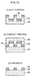
- a transfer process as illustrated in Fig. 12 has also been proposed. More specifically, an Au film 32 is formed on an Si substrate 30, and, separately, an alkanethiol film 34 is provided on a concave and convex pattern surface of a master 36 formed with PDMS (polydimethylsiloxane). Then, the alkanethiol film 34 on the convex portions is bonded to the Au film 32 for transferring.
- PDMS polydimethylsiloxane
- the Au film 32 and the substrate 30 at a portion which is not masked by the alkanethiol film 34 are etched, and thus the pattern of the Au film 32 remains on a portion which is masked by the alkanethiol film 34.
- RIE reactive ion etching
- JP 2 303 820 A and JP 2 073987 A disclose methods for duplicating stamples.
- the present invention provides the following process for producing a structure with a metal film, a mother die for use in the process, and a structure produced by the process.
- a first aspect of the invention provides a process for producing a structure with a metal film, including:
- a second aspect of the invention provides a mother die, having:
- a concave and convex pattern to be transferred (hereinafter sometimes referred to as a "transfer pattern" or a "pattern") is formed beforehand on the surface of a base serving as a mother die, subsequently a first metal film serving as a protective film is formed on the surface on which the transfer pattern has been formed, a second metal film is further formed thereon in such a manner as not to chemically bond to the first metal film, and the second metal film is transferred to a support member, the second metal film to which the transfer pattern has been transferred can be securely transferred to the support member side and also the second metal film can be repeatedly transferred while preventing damages to the fine concave and convex pattern of the mother die.
- the present invention has been accomplished.
- Fig. 1 shows an example of a process for producing a structure with a metal film according to the present invention. More specifically, the process for producing a structure with a metal film according to the invention, includes:
- a mother die (master) 10 in which a first metal film (protective film) 16 is formed on the surface of a base 12 on which a concave and convex pattern 14 is formed is prepared ( Fig. 1 (A) ).
- the material or shape of the base 12 serving as the body of the mother die 10 is not particularly limited insofar as the concave and convex pattern 14 to be transferred to the second metal film 18 later can be formed and the first metal film 16 and the second metal film 18 can be successively formed on the surface on which the concave and convex pattern 14 is formed.
- the material (mold material) of the base 12 include silicon, glassy carbon, quartz, ceramics, and metals from the viewpoints of the formability of the pattern 14, the mechanical strength and heat resistance as the mother die 10, the film formability of the metal film and the like.
- the concave and convex pattern 14 on the surface of the base 12 may be formed according to the purpose, and the concave and convex pattern 14 may be formed as desired on the surface of the base 12 by, for example, lithography, electron beam processing, ion beam processing and the like.
- a desired circuit pattern can be formed on the surface (one side) of the base 12, such as a silicon substrate, by, for example, lithography (photo lithography, electron-beam lithography, etc.) and etching.
- an SOG Spin on Glass
- a flat substrate such as a silicon substrate, and then can be formed into a concave and convex pattern.
- fine projections of nm order can be formed at the surface (processed surface) of the base 12 by ion beam processing of the base 12, such as glassy carbon (GC).
- a pattern containing fine projections having a shape in which the diameter decreases from the bottom towards the top end thereof, such as a needle shape, a conical shape, or a pyramid shape, can be formed.
- Such a transfer pattern containing projections having a shape in which the diameter decreases from the bottom towards the top end thereof is advantageous in that transfer (separation) is facilitated rather than a transfer pattern containing projections in which the diameter is almost fixed, such as a cylindrical shape.
- the height or the pitch of the projections to be formed at the surface of the base can be controlled to some extent by adjusting the processing time, acceleration voltage, and gas flow rate (see JP-A No. 2008-233850 ).
- the first metal film 16 constitutes the mother die 10 with the base 12
- the first metal film 16 is formed with metals (simple metals or metal compounds, such as alloys or metal oxides) having high adhesiveness with materials constituting the base 12 (hereinafter referred to as a mold material) and not chemically bonding to the second metal film 18 to be formed on the first metal film 16 in the following step.
- the first metal film 16 is preferably a film that forms a compound with the mold material and forms an intermediate layer.
- a film containing chromium (Cr) is mentioned.
- the mold material is quartz
- a film is formed using Cr on the quartz, a chrome oxide (Cr 2 O 3 ) that is stable as an intermediate layer is formed, and a Cr film having high adhesiveness is obtained.
- the mold material is SOG
- a stable chrome oxide is similarly formed and a Cr film having high adhesiveness is obtained.
- chromium carbide (Cr 2 C 3 , CrC) is formed as an intermediate layer when chromium is formed on the surface, and then a Cr film having high adhesiveness is similarly obtained.
- the first metal film 16 is not limited to the Cr film, and materials may be selected according to adhesiveness with mold materials and ease of separation from the second metal film 18.
- the first metal film 16 is preferably a film containing metal compounds, such as metal oxides or metal carbides, rather than a film containing simple metals, and metal oxide films are particularly preferable.
- Metals constituting the first metal film 16 are preferably aluminum (Al) in addition to Cr. It is estimated that both Cr and Al are naturally oxidized in the air and stabilized after formed into films to be closely adhered to the base 12 and also the chemical bonding with the second metal film 18 is suppressed, which facilitates the separation of the second metal film 18.
- the first metal film 16 may be intentionally subjected to oxidation treatment, nitriding treatment, carbonization treatment, etc., to be formed into a film containing metal compounds.
- Methods for forming the first metal film 16 are not particularly limited. Preferable examples include vapor deposition, coating, and plating. The film forming methods may be selected according to the materials of the first metal film 16 and the mold materials constituting the base 12. The thickness of the first metal film 16 may be determined according to, for example, the pitch P of the concave and convex pattern 14 of the base 12. When the thickness of the first metal film 16 is excessively thin, the first metal film does not sufficiently function as a protective film and thus the concave and convex pattern 14 may be partially damaged by transfer.
- the thickness of the first metal film 16 depends on the pitch P between the convex portions of the transfer pattern 14 and is preferably 1 to 3000 nm, more preferably 3 to 1000 nm, and particularly preferably 5 to 100 nm.
- the mother die 10 constituted by the base 12 and the first metal film 16 described above is prepared, and then the second metal film 18 is formed on the first metal film 16 ( Fig. 1(B) ).
- the second metal film 18 is formed on the first metal film 16 formed on the transfer pattern surface side of the base 12. Since the second metal film 18 is separated from the first metal film 16 after the support member 20 is adhered in a transfer step later, the second metal film 18 is formed with metals (simple metals or metal compounds, such as alloys or metal oxides) that do not chemically bond to the first metal film 16.
- the second metal film 18 may be selected according to the purpose of a structure 22 having the metal film 18 to be obtained after transfer. Examples of the second metal film 18 include films containing at least one metal selected from the group consisting of Au, Ag, Cu, Al, and Pt.
- the second metal film 18 is a metal film which contains such materials and to which the transfer pattern 14 of the mother die 10 has been transferred, the film can serve as, for example, a functional film having functions of a catalyst and the like.
- a Cr film is formed as the first metal film 16
- an alloy or the like with Cr is not produced and thus the second metal film 18 can be relatively easily transferred (separated).
- an Al film is formed as the first metal film 16
- a film containing Cu or constantan (alloy of Ni and Cu) as metals constituting the second metal film 18 is preferable and a Cu film is particularly preferable.
- the second metal film 18 is not limited to films containing the metals mentioned above and the materials thereof may be selected according to the purpose.
- Film forming methods for the second metal film 18 are not limited insofar as a film can be formed with a desired thickness in such a manner as not to chemically bond to the first metal film 16, and may be selected considering the materials constituting the second metal film 18, the materials constituting the first metal film 16, and the mold materials constituting the base 12. It is preferable to form the second metal film 18 by vapor deposition, coating, or plating from the viewpoints of ease of film formation, film thickness uniformity, etc.
- the thickness of the second metal film 18 is not particularly limited. When the thickness of the second metal film 18 is excessively thin, the film may be damaged in the transfer process. When the thickness thereof is excessively thick, an increase in the cost or poor transfer may be caused. Considering the above respects, the thickness of the second metal film 18 depends on the pitch P between the convex portions of the transfer pattern 14 and is preferably 10 to 3000 nm, more preferably 50 to 2000 nm, and particularly preferably 100 to 1500 nm.
- a mold release agent may be supplied between the first metal film 16 and the second metal film 18.
- the mold release agent include a silane coupling agent.
- the second metal film 18 is formed on the first metal film 16, and then the support member 20 is adhered to the second metal film 18 ( Fig. 1(C) ).
- the support member 20 Since the support member 20 is adhered to the second metal film 18 and separated from the first metal film 16, the support member 20 may be selected according to adhesiveness with the second metal film 18 and the purpose after transfer.
- resin and glass can be preferably used.
- the resin include resins that have fluidity before supplied to the second metal film 18, thereby can be easily supplied, and that may be cured by the application of external energy, such as light or heat after supplied, and ultraviolet curable resins are particularly preferable.
- Methods for supplying a curable resin are not particularly limited, and may be suitably selected from known coating methods, such as squeegee coating or spin coating, according to the viscosity or the like of a curable material.
- the resin When an ultraviolet curable resin is applied to the second metal film 18, the resin is irradiated with ultraviolet ray of photosensitive wavelength for curing.
- a thermosetting resin When a thermosetting resin is used, the resin is heated to a given temperature for curing. Even when the concave and convex pattern has a high aspect ratio (e.g., 2 or more), the use of a curable resin composition which is in the form of liquid at room temperature allows preferable charging and curing thereof between the convex portions. In this case, the resin can be adhered throughout the second metal film formed on the mother die 10. After curing, the second metal film 18 formed between the convex portions can also be preferably transferred to the support member 20. Moreover, a resin film (PET film or the like) that is softened by heating while being in contact with the second metal film 18, and then is adhered to the second metal film 18 when cured by cooling can also be used.
- PET film or the like that is softened by heating while being in contact with the second metal film 18, and then is adhere
- a glass material such as SOG (Spin on Glass) can also be preferably used as the support member 20.
- SOG spin on Glass
- the SOG can be spin coated onto the metal film, and then can be baked at relatively low temperatures (e.g., 250 to 500°C).
- relatively low temperatures e.g. 250 to 500°C.
- the support member 20 is adhered to the second metal film 18, and then the second metal film 18, to which the concave and convex pattern 14 has been transferred, is separated with the support member 20 from the first metal film 16 ( Fig. 1 (D) ).
- the second metal film 18 is transferred to the support member 20 side, thereby obtaining a structure 22 having the second metal film 18 to which the transfer pattern 14 of the base 12 has been transferred.
- the transfer pattern 14 of the base 12 is transferred to the surface of the second metal film 18.
- the second metal film 18 is a film to which a film formed through the first metal film 16 has been transferred. Therefore, the surface state is favorable compared with a film formed on the surface of the base 12 on which the transfer pattern 14 has been formed directly or only through a mold release agent, and then transferred. For example, even in the case of a circuit pattern having a line width of nm order, disconnection can be effectively prevented.
- the fine structure of the base 12 is transferred with favorable precision to the surface of the first metal film 16 after transfer, thereby obtaining the structure 22 having the second metal film 18 whose surface area is extremely large.
- the mother die 10 after transfer can be repeatedly used as a mother die, because the transfer pattern 14 is protected by the first metal film 16, and thus, damages when the second metal film 18 is separated are suppressed. More specifically, by successively repeating, after transfer, (B) the formation of the second metal film 18 on the first metal film 16, (C) the adhesion of the support member 20 to the second metal film 18, and (D) the separation between the first metal film 14 and the second metal film 18, the structure 22 having the second metal film to which the transfer pattern 14 of the base 12 has been transferred can be mass produced at a low cost.
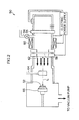
- the surface of a substrate (Thickness: 1 mm, Length and Width: 10 mm ⁇ 10 mm) of glassy carbon whose surface was polished (manufactured by Tokai Carbon Co., Ltd.) was subjected to ion beam processing using an ECR (Electron Cyclotron Resonance) type ion beam processing device (trade name: EIS-200ER, manufactured by Elionix Co., Ltd.) having the structure illustrated in Fig. 2 .
- ECR Electro Cyclotron Resonance
- An ion beam processing device 50 for use in the ion beam processing has a holder 66 for holding a substrate 52, a gas introduction pipe 54, a plasma generating chamber 56, an extractor 58, an electromagnet 60, an ion beam withdrawing electrode 62, a Faraday cup 64, etc.
- the current density becomes low at a low acceleration voltage of, for example, 500 V or lower, and thus, in order to increase the current density, the extractor 58 functions as a grid for withdrawing ions at a plasma side from the withdrawing electrode 62.
- the current density becomes high to increase the processing speed even when the acceleration voltage is low.
- the glassy carbon substrate (GC substrate) 52 is placed on the holder 66, oxygen was introduced as a reactant gas, and also a given acceleration voltage is applied, thereby subjecting the surface of the GC substrate 52 to ion beam processing.
- the processing conditions are as follows.
- Fig. 3 shows SEM images showing the surface state of the GC substrate that was processed while changing the processing time.
- a pattern containing fine projections having a shape in which the diameter decreases towards the top end is formed, and the height and pitch of the projections changed according to the processing time.
- chromium (Cr) film was formed on the processed surface of the GC substrate that was processed by ECR for 5 minutes.
- a 20 nm thick Cr deposited film was formed using a vacuum deposition device (trade name: CPC-260F, manufactured by Shinku Kiko Co., Ltd).
- Fig. 4(A) shows SEM images after a Cr deposited film was formed on the fine pattern surface of the GC substrate.
- Fig. 4 (B) shows an SEM image after the Au film was formed.
- a photocurable resin (trade name: PAK-01, manufactured by Toyo Gosei Co., Ltd.) was spin coated onto the Au film.
- PAK-01 manufactured by Toyo Gosei Co., Ltd.
- a slide glass was pressed against the PAK-01 coated surface under the following conditions, and ultraviolet light was emitted from the slide glass side to cure the PAK-01.
- Fig. 5 shows an SEM image of the Au film transferred onto the slide glass through the PAK-01, which shows that fine projection-like convex and concave portions are formed on the Au film.
- Fig. 6 shows an SEM image showing the mother die after separation, which shows that the projections are not damaged.
- the processing, film formation, and transfer were performed in a manner substantially similar to that in Example 1-1, except changing the processing time of the GC substrate to 10 minutes or 15 minutes.
- the GC substrate was subjected to ion beam processing in a manner substantially similar to that in Example 1-1, and then a mold release agent (trade name: DURASURF HD-1101Z, manufactured by HARVES Co., Ltd.) was applied to the processed surface. Subsequently, a photocurable resin (trade name: PAK-01, manufactured by Toyo Gosei Co., Ltd.) was spin coated thereto. The PAK-01 coated surface was pressed against a slide glass, and simultaneously ultraviolet light was emitted under the same conditions as that in Example 1 to cure the PAK-01. After curing, the slide glass and the GC substrate were slowly separated from each other.
- a mold release agent trade name: DURASURF HD-1101Z, manufactured by HARVES Co., Ltd.
- PAK-01 photocurable resin
- the processing, coating of a mold release agent, and transfer were performed in a manner substantially similar to that in Comparative Example 1-2, except changing the processing time of GC substrate to 10 minutes.
- the GC substrate was subjected to ion beam processing in a manner substantially similar to that in Example 1-1, and then an Au film was directly formed on the processed surface.
- a 70 nm thick Au deposited film was formed using a vacuum deposition device (trade name: CPC-260F, manufactured by Shinku Koki Co., Ltd).
- a photocurable resin (trade name: PAK-01, manufactured by Toyo Gosei Co., Ltd.) was spin coated onto the Au film. A slide glass was pressed against the PAK-01 coated surface, and simultaneously ultraviolet light was emitted under the same conditions in Example 1 to cure the PAK-01.
- the processing, film formation, and transfer were performed in a manner substantially similar to that in Comparative Example 2-1, except changing the processing time of the GC substrate to 10 minutes or 15 minutes.
- Example 1-1 The transfer results in Example 1-1 to Comparative Example 2-3 above are shown in Table 1.
- the transfer evaluation in Table 1 is as follows.
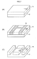
- an SOG (trade name: ACCUGLASS (registered trademark) 512B, manufactured by Honeywell, Inc.)13 was spin coated onto an Si wafer 12, and baked (pre-heating: 80°C for 3 minutes, main heating: 425°C for 1 hour). Subsequently, as illustrated in Fig. 7(B) , a resist was applied and arbitrary portions 15 were irradiated with an electron beam (acceleration voltage: 30 kV, dose: 2000 to 5500 ⁇ C/cm 2 ).
- the resultant was immersed in a BHF (2.4% for 2 minutes) as a developer so that the electron beam-irradiated portion dissolved to form a concave portion, thereby obtaining a mold in which the concave and convex pattern 14 of SOG was formed on the Si substrate 12 as illustrated in Fig. 7(C) .
- the smallest gap between the convex portions of the concave and convex pattern of the mold is 110 nm.
- the Cr deposited film 16 (thickness: 10 nm) was formed on the obtained mold, and the Au deposited film 18 (thickness: 60 nm) was further formed thereon.
- the PET substrate 20 was brought into contact with the Au film 18, and heated at 80°C for 30 minutes, thereby performing contact printing. Furthermore, after cooling, the PET substrate 20 was slowly separated to thereby transfer the Au film 18 to the surface of the PET substrate 20 as illustrated in Fig. 8(F) .
- a fluorocarbon-based resin coating agent (trade name: DURASURF HD-1101Z, manufactured by HARVES Co., Ltd.) 24 as a mold release agent was applied to the pattern formation side, and then the Au deposited film 18 was formed thereon.
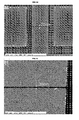
- Fig. 10 shows an SEM image showing the surface state of the Au films each formed in Example 2 and Comparative Example 3.
- the Au film ( Fig. 10(b) ) formed in Example 2 was smooth.
- Fig. 11 shows an SEM image obtained by observing the Au film after transferred to the PET substrate in Example 2.
- the PET film did not sag and was formed without disconnection even in the case of an Au pattern having a line width of about 70 nm.
- a mold was produced in a manner substantially similar to that in Example 2, except changing the smallest gap between the convex portions of the mold to 70 nm as illustrated in Fig. 14 .
- a Cr deposited film (thickness: 10 nm) was formed to the concave and convex pattern surface of the mold to further form an Au deposited film (thickness: 60 nm).
- the Au film was transferred to the PET film in a manner substantially similar to that in Example 2.
- Fig. 15 shows an SEM image of the Au film transferred to the PET film. The Au film was transferred without disconnection of the line of the Au film, and the gap between the lines of about 30 nm is secured.
- An SOG (trade name: ACCUGLASS (registered trademark) 512B, manufactured by Honeywell, Inc.) was spin coated onto an Si wafer 12, and baked to form an SOG layer (thickness: 500 nm). Arbitrary portions of the SOG layer were irradiated with an electron beam, thereby obtaining a mold on which a concave and convex pattern was formed. In the process, the line width of the electron beam was adjusted to 400 nm, and the depth of the concave portions (grooves) was changed by changing a voltage. Subsequently, an Al deposited film (thickness: 20 nm) was formed on the SOG concave and convex pattern surface, and a Cu deposited film (thickness: 500 nm) was further formed.
- the PET substrate was brought into contact with the Cu film, and heated at 90°C for 30 minutes, thereby performing contact printing. After cooling, the PET substrate 20 was slowly separated to thereby transfer the Cu film to the surface of the PET substrate. Thus, the Cu pattern to which the concave and convex pattern of the SOG layer was transferred was transferred onto the PET substrate.
- a SOG concave and convex pattern The formation of a SOG concave and convex pattern, film formation of an Al deposited film, film formation of a Cu deposited film, and the transfer of the Cu film to the PET substrate were successively performed in a manner substantially similar to that in Example 4-1, except changing the line width of the electron beam to 300 nm, 200 nm, or 100 nm when forming the SOG concave and convex pattern.
- Fig. 19 shows SEM images of the Cu pattern transferred onto the PET substrate when the line width was adjusted to 200 nm and 100 nm, respectively. In both the cases, the Cu pattern to which the concave and convex pattern of the SOG layer was transferred is transferred onto the PET substrate.
- Fig. 19 shows SEM images in which the measurement groove width (gap between lines) of the Cu pattern is 75 nm (in the case of the designed width of 200 nm) or 40 nm (in the case of the designed width of 100 nm), respectively.
- An SOG layer was formed on an Si substrate in a manner substantially similar to that in Example 4-1, and the second metal film was transferred to the PET substrate by variously changing the first metal film and the second metal film.
- the transfer state is evaluated by SEM images and the results are shown in Table 2.
- Cu-Ni in Table 2 represents constantan (alloy of copper and nickel), and the evaluation criteria for A, B, and C is as follows.
- a first metal film and a second metal film were successively formed on an Si substrate without forming an SOG layer, and then the second metal film was transferred to a PET substrate.
- the results are shown in Table 3. The evaluation is performed in a manner substantially similar to that in Example 5.
- a mold was produced in a manner substantially similar to that in Example 2, and then a Cr deposited film (thickness: 22 nm) and an Au deposited film (thickness: 50 nm) were successively formed on the pattern surface of the mold. Thereafter, the Au film was transferred to the PET film in a manner substantially similar to that in Example 2.
- the mold surface was analyzed by SEM-EDX. As an SEM-EDX, "ERAX-8900" (trade name), manufactured by Elionix, Inc. was used.
- Fig. 16(A) shows the analysis results before transfer and Fig. 16(B) shows the analysis results after transfer. The comparison of the results before and after transfer shows that, after transfer, Au sharply decreases and Cr almost remains.
- An SOG (trade name: ACCUGLASS (registered trademark) 512B, manufactured by Honeywell, Inc.) was spin coated onto an Si wafer, and baked (pre-heating: 80°C for 3 minutes, main heating: 425°C for 1 hour). Subsequently, a Cr deposited film (thickness: 18 nm) was formed, and an Au deposited film (thickness: 50 nm) was further formed. Then, the Au film was transferred to the PET film in a manner substantially similar to that in Example 2.
- SOG trade name: ACCUGLASS (registered trademark) 512B, manufactured by Honeywell, Inc.
- Fig. 17 illustrates the analysis results of XPS. Near the outermost surface indicated by Arrow A, a chromium oxide film, such as Cr 2 O 3 , is formed, and it is considered that the chromium oxide film is effective for mold releasing a gold layer. Then, it is considered that, in a portion where O decreases and Cr increases relative to the outermost surface, a Cr oxide decreases and, in contrast, the proportion of a Cr metal increases.
- a chromium oxide film such as Cr 2 O 3
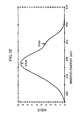
- Fig. 18 shows a spectrum separation ratio of Cr in the outermost surface, the peak of Cr 2 O 3 appears at 576.6 eV and the peak of Cr metal appears at 574.3 eV. It is considered from the graph that a Cr oxide film is mainly formed on the outermost surface.
- the process for producing a structure with a metal film according to the present invention can be applied to various applications.
- the second metal film obtained after transfer becomes extremely advantageous when used as a catalyst surface or the like because the fine pattern of the mother die is transferred, and thus the surface area can become extremely large.
- the second metal film becomes extremely useful as a catalyst.
- the second metal film formed in convex portions of a mold is transferred to the PET substrate.
- metal wiring is relatively easily formed on an insulating substrate, and the second metal film can be advantageously applied when producing a wire grid polarizer, a plasmon element, etc.
- the second metal may be dissolved with an appropriate solvent after transfer.
- resins are charged by SEM observation, when the pattern of the support member after transfer is observed by SEM, the charging can be prevented when the resin is covered with a metal film. Therefore, it is considered that the present invention is also effective in a process for reproducing a mold (replica mold production process).
- the reflection prevention structure according to the present invention is described, but the present invention is not limited to the embodiments and the Examples above.
- other processing devices such as ICP, may be used while not limited to the ECR type ion beam processing device as illustrated in Fig. 2 .
Landscapes
- Chemical & Material Sciences (AREA)
- Engineering & Computer Science (AREA)
- Organic Chemistry (AREA)
- Materials Engineering (AREA)
- Mechanical Engineering (AREA)
- Metallurgy (AREA)
- Chemical Kinetics & Catalysis (AREA)
- Manufacturing & Machinery (AREA)
- Microelectronics & Electronic Packaging (AREA)
- Physics & Mathematics (AREA)
- Plasma & Fusion (AREA)
- Shaping Of Tube Ends By Bending Or Straightening (AREA)
- Manufacturing Of Printed Wiring (AREA)
- Moulds For Moulding Plastics Or The Like (AREA)
- Physical Vapour Deposition (AREA)
Claims (13)
- Verfahren zum Herstellen einer Struktur mit einer Metallschicht, mit den Schritten:Bereitstellen einer Matrize (10), in der eine erste Metallschicht (16) auf der Oberfläche einer Basis (12) ausgebildet ist, auf der ein konkaves und konvexes Muster (14) ausgebildet ist;Ausbilden einer zweiten Metallschicht (18) auf der ersten Metallschicht (16) derart, dass das konkave und konvexe Muster (14) auf die zweite Metallschicht (18) übertragen werden;Anhaften eines Trägerelements (20) an der zweiten Metallschicht (18); undTrennen der zweiten Metallschicht (18) und des Trägerelements (20) von der ersten Metallschicht (16);dadurch gekennzeichnet, dassdie erste Metallschicht (16) eine Schicht ist, die Chrom oder Aluminium enthält.
- Verfahren nach Anspruch 1, wobei die erste Metallschicht (16) eine Lage aus einem Metalloxid oder einem Metallcarbid enthält, das ein Reaktionsprodukt einer Reaktion eines die Basis bildenden Atoms an einer Grenzfläche mit der Basis ist.
- Verfahren nach Anspruch 1 oder 2, wobei die erste Metallschicht (16) an seiner äußersten Oberfläche eine Lage aus einem Metalloxid, einem Metallnitrid oder einem Metallcarbid enthält.
- Verfahren nach einem der Ansprüche 1 bis 3, wobei die zweite Metallschicht (18) eine Schicht ist, die mindestens ein Metall enthält, das aus Au, Ag, Cu, Al und Pt ausgewählt wird.
- Verfahren nach einem der Ansprüche 1 bis 4, wobei die zweite Metallschicht (18) durch Aufdampfen, Beschichten oder Plattieren ausgebildet wird.
- Verfahren nach einem der Ansprüche 1 bis 5, ferner mit dem Zuführen eines Formentrennmittels zwischen die erste Metallschicht (16) und die zweite Metallschicht (18).
- Verfahren nach einem der Ansprüche 1 bis 6, wobei als die Basis (12) eine Glaskohlenstoff enthaltende Basis verwendet wird.
- Verfahren nach einem der Ansprüche 1 bis 7, wobei das konkave und konvexe Muster (14) ein Muster ist, das Vorsprünge mit einer Form enthält, in der der Durchmesser zum oberen Ende hin abnimmt.
- Struktur mit der durch das Verfahren nach einem der Ansprüche 1 bis 8 hergestellten zweiten Metallschicht.
- Matrize (10) mit:einer Basis (12); an deren Oberfläche ein konkaves und konvexes Muster (14) ausgebildet ist; undeiner auf der Oberfläche der Basis, auf der das konkave und konvexe Muster (14) ausgebildet ist, ausgebildeten Metallschicht;dadurch gekennzeichnet, dassdie Metallschicht Chrom oder Aluminium enthält.
- Matrize (10) nach Anspruch 10, wobei die Metallschicht eine Lage aus einem Metalloxid oder einem Metallcarbid enthält, das ein Reaktionsprodukt mit einem die Basis (12) bildenden Atom an einer Grenzfläche mit der Basis (12) ist.
- Matrize (10) nach Anspruch 10 oder 11, wobei die Metallschicht an seiner äußersten Oberfläche eine Lage aus einem Metalloxid, einem Metallnitrid oder einem Metallcarbid enthält.
- Matrize (10) nach einem der Ansprüche 10 bis 12, wobei das konkave und konvexe Muster (14) ein Muster ist, das Vorsprünge mit einer Form enthält, in der der Durchmesser zum oberen Ende hin abnimmt.
Applications Claiming Priority (3)
| Application Number | Priority Date | Filing Date | Title |
|---|---|---|---|
| JP2008029631 | 2008-02-08 | ||
| JP2008233873 | 2008-09-11 | ||
| PCT/JP2009/052183 WO2009099235A1 (ja) | 2008-02-08 | 2009-02-09 | 金属膜を有する構造体の製造方法、それに用いる母型及びそれにより製造される構造体 |
Publications (3)
| Publication Number | Publication Date |
|---|---|
| EP2242341A1 EP2242341A1 (de) | 2010-10-20 |
| EP2242341A4 EP2242341A4 (de) | 2011-12-28 |
| EP2242341B1 true EP2242341B1 (de) | 2013-12-11 |
Family
ID=40952298
Family Applications (1)
| Application Number | Title | Priority Date | Filing Date |
|---|---|---|---|
| EP09708441.2A Not-in-force EP2242341B1 (de) | 2008-02-08 | 2009-02-09 | Verfahren zur herstellung einer struktur mit einem metallfilm, vorlagenmatrize zur verwendung in diesem verfahren und in dem verfahren hergestellte struktur |
Country Status (4)
| Country | Link |
|---|---|
| US (1) | US9332651B2 (de) |
| EP (1) | EP2242341B1 (de) |
| JP (2) | JP5569927B2 (de) |
| WO (1) | WO2009099235A1 (de) |
Families Citing this family (6)
| Publication number | Priority date | Publication date | Assignee | Title |
|---|---|---|---|---|
| JP5624933B2 (ja) * | 2010-04-28 | 2014-11-12 | Hoya株式会社 | X線による性能評価方法およびその利用 |
| US11013835B2 (en) * | 2012-02-03 | 2021-05-25 | Board Of Regents, The University Of Texas System | Processability of polymeric substrates and related methods |
| WO2016021533A1 (ja) * | 2014-08-04 | 2016-02-11 | Jx日鉱日石エネルギー株式会社 | 凹凸パターンを有する部材の製造方法 |
| JP6918631B2 (ja) * | 2017-08-18 | 2021-08-11 | 浜松ホトニクス株式会社 | 光検出素子 |
| WO2019202650A1 (ja) * | 2018-04-17 | 2019-10-24 | 株式会社 日立ハイテクノロジーズ | 顕微鏡用スライド、顕微鏡用スライドの製造方法、観察方法及び分析方法 |
| JP6948369B2 (ja) * | 2018-11-06 | 2021-10-13 | 学校法人東京理科大学 | モスアイ転写型及びモスアイ転写型の製造方法 |
Family Cites Families (23)
| Publication number | Priority date | Publication date | Assignee | Title |
|---|---|---|---|---|
| US4116753A (en) * | 1976-06-14 | 1978-09-26 | Olympus Optical Co., Ltd. | Method for the manufacture of optical mold for reproducing curved surfaces having the same shape as an optical prototype |
| JPS5952715B2 (ja) * | 1977-09-05 | 1984-12-21 | ソニー株式会社 | メツキ方法 |
| JPS5835742A (ja) * | 1981-08-21 | 1983-03-02 | Victor Co Of Japan Ltd | 情報記録媒体円盤の製作に用いられるスタンパの製作法 |
| JPS63112842A (ja) * | 1986-10-28 | 1988-05-17 | Seiko Epson Corp | 光デイスク基板複製用スタンバ−の製造方法 |
| JPH0273987A (ja) | 1988-09-09 | 1990-03-13 | Seiko Epson Corp | スタンパの複製方法 |
| JPH02303820A (ja) | 1989-05-18 | 1990-12-17 | Ricoh Co Ltd | スタンパの複製方法 |
| US5388803A (en) * | 1993-08-17 | 1995-02-14 | General Electric Company | Apparatus for producing textured articles |
| JPH10330123A (ja) | 1997-05-27 | 1998-12-15 | Asahi Glass Co Ltd | ガラス成形用金型及びガラス成形方法 |
| US6814897B2 (en) * | 1998-03-27 | 2004-11-09 | Discovision Associates | Method for manufacturing a molding tool used for substrate molding |
| US6190838B1 (en) * | 1998-04-06 | 2001-02-20 | Imation Corp. | Process for making multiple data storage disk stampers from one master |
| JP2000327344A (ja) * | 1999-05-17 | 2000-11-28 | Olympus Optical Co Ltd | 光学素子成形用型の製造方法及び光学素子成形用型 |
| JP3694825B2 (ja) * | 1999-11-18 | 2005-09-14 | 日本航空電子工業株式会社 | 導体パターンの形成方法及びコネクタ、フレキシブルプリント配線板、異方導電性部材 |
| JP2002020129A (ja) | 2000-07-03 | 2002-01-23 | Olympus Optical Co Ltd | 光学素子成形用型及びその製造方法 |
| JP2004063694A (ja) | 2002-07-26 | 2004-02-26 | Seiko Epson Corp | パターン転写フィルム、パターン転写フィルムの製造方法、機能性マスク、機能性マスクの製造方法 |
| JP4193479B2 (ja) | 2002-12-04 | 2008-12-10 | ソニー株式会社 | 素子実装基板の製造方法 |
| JP4284106B2 (ja) | 2003-05-15 | 2009-06-24 | コバレントマテリアル株式会社 | シリカガラスの成形方法 |
| JP2005051095A (ja) | 2003-07-30 | 2005-02-24 | Tdk Corp | 転写用基体およびその製造方法 |
| JP4430959B2 (ja) | 2004-02-27 | 2010-03-10 | 東海カーボン株式会社 | 成形型 |
| JP2005340432A (ja) | 2004-05-26 | 2005-12-08 | Shinko Electric Ind Co Ltd | 配線基板の製造方法 |
| JP2006150741A (ja) | 2004-11-29 | 2006-06-15 | Asahi Glass Co Ltd | 転写層にパターンを形成する方法 |
| JP4371048B2 (ja) | 2004-12-21 | 2009-11-25 | コニカミノルタオプト株式会社 | 光学ガラス成形用金型及び光学ガラス素子 |
| JP2006196768A (ja) | 2005-01-14 | 2006-07-27 | Shinko Electric Ind Co Ltd | 配線基板の製造方法 |
| US7287325B2 (en) * | 2005-05-10 | 2007-10-30 | International Business Machines Corporation | Method of forming interconnect structure or interconnect and via structures using post chemical mechanical polishing |
-
2009
- 2009-02-09 JP JP2009552564A patent/JP5569927B2/ja not_active Expired - Fee Related
- 2009-02-09 US US12/675,537 patent/US9332651B2/en not_active Expired - Fee Related
- 2009-02-09 EP EP09708441.2A patent/EP2242341B1/de not_active Not-in-force
- 2009-02-09 WO PCT/JP2009/052183 patent/WO2009099235A1/ja not_active Ceased
-
2014
- 2014-03-03 JP JP2014040990A patent/JP5769216B2/ja not_active Expired - Fee Related
Also Published As
| Publication number | Publication date |
|---|---|
| US9332651B2 (en) | 2016-05-03 |
| EP2242341A1 (de) | 2010-10-20 |
| JPWO2009099235A1 (ja) | 2011-06-02 |
| EP2242341A4 (de) | 2011-12-28 |
| JP5769216B2 (ja) | 2015-08-26 |
| JP2014144639A (ja) | 2014-08-14 |
| JP5569927B2 (ja) | 2014-08-13 |
| WO2009099235A1 (ja) | 2009-08-13 |
| US20100308204A1 (en) | 2010-12-09 |
Similar Documents
| Publication | Publication Date | Title |
|---|---|---|
| EP2242341B1 (de) | Verfahren zur herstellung einer struktur mit einem metallfilm, vorlagenmatrize zur verwendung in diesem verfahren und in dem verfahren hergestellte struktur | |
| US7022465B2 (en) | Method in connection with the production of a template and the template thus produced | |
| JP4791357B2 (ja) | 成形される領域と成形型のパターンとの間の接着を低減させる方法 | |
| JP3161362B2 (ja) | 微小構造体、その製造方法、その製造装置、基板および成形型 | |
| TWI278488B (en) | Contact planarization materials that generate no volatile byproducts or residue during curing | |
| TWI628516B (zh) | 採用具有金屬或氧化物塗層之可重複使用聚合物模板的奈米壓印技術 | |
| US20050084804A1 (en) | Low surface energy templates | |
| TWI335490B (en) | Nano-imprinting process | |
| US11903141B2 (en) | Method for manufacturing wiring board | |
| JP2009149097A (ja) | インプリント加工用スタンパーおよびその製造方法 | |
| EP3262677B1 (de) | Filmelektrode für elektrostatischen chuck | |
| GB2050218A (en) | Process for forming electroconductive patterns on non-conductive substrates | |
| JP6710018B2 (ja) | 導電パターン基板の製造方法 | |
| JP2006032423A (ja) | インプリント加工用スタンパーおよびその製造方法 | |
| CN101762978A (zh) | 抗蚀剂 | |
| US20060216413A1 (en) | Mold and process of production thereof | |
| JP3627482B2 (ja) | 微小構造体の製造方法 | |
| JP2019083347A (ja) | 導電パターン基板の製造方法 | |
| JP3612945B2 (ja) | 微小構造体の製造方法 | |
| JPH11221829A (ja) | 薄膜形成用基板及び微小構造体の製造方法 | |
| JP2003185674A (ja) | プローブユニットおよびその製造方法 | |
| JP3627486B2 (ja) | 微小構造体の製造方法 | |
| US20050139475A1 (en) | Insert dies, molds, and methods for fabricating the same | |
| JP5186663B2 (ja) | 微細構造の製造方法および回路基盤の製造方法 | |
| JP2005212028A (ja) | 微小構造体の製造方法および装置 |
Legal Events
| Date | Code | Title | Description |
|---|---|---|---|
| PUAI | Public reference made under article 153(3) epc to a published international application that has entered the european phase |
Free format text: ORIGINAL CODE: 0009012 |
|
| 17P | Request for examination filed |
Effective date: 20100316 |
|
| AK | Designated contracting states |
Kind code of ref document: A1 Designated state(s): AT BE BG CH CY CZ DE DK EE ES FI FR GB GR HR HU IE IS IT LI LT LU LV MC MK MT NL NO PL PT RO SE SI SK TR |
|
| AX | Request for extension of the european patent |
Extension state: AL BA RS |
|
| DAX | Request for extension of the european patent (deleted) | ||
| A4 | Supplementary search report drawn up and despatched |
Effective date: 20111124 |
|
| RIC1 | Information provided on ipc code assigned before grant |
Ipc: H05K 3/20 20060101AFI20111118BHEP Ipc: B32B 15/04 20060101ALI20111118BHEP |
|
| GRAP | Despatch of communication of intention to grant a patent |
Free format text: ORIGINAL CODE: EPIDOSNIGR1 |
|
| INTG | Intention to grant announced |
Effective date: 20130607 |
|
| GRAS | Grant fee paid |
Free format text: ORIGINAL CODE: EPIDOSNIGR3 |
|
| GRAA | (expected) grant |
Free format text: ORIGINAL CODE: 0009210 |
|
| AK | Designated contracting states |
Kind code of ref document: B1 Designated state(s): AT BE BG CH CY CZ DE DK EE ES FI FR GB GR HR HU IE IS IT LI LT LU LV MC MK MT NL NO PL PT RO SE SI SK TR |
|
| REG | Reference to a national code |
Ref country code: GB Ref legal event code: FG4D |
|
| REG | Reference to a national code |
Ref country code: CH Ref legal event code: EP |
|
| REG | Reference to a national code |
Ref country code: AT Ref legal event code: REF Ref document number: 645143 Country of ref document: AT Kind code of ref document: T Effective date: 20140115 |
|
| REG | Reference to a national code |
Ref country code: IE Ref legal event code: FG4D |
|
| REG | Reference to a national code |
Ref country code: DE Ref legal event code: R096 Ref document number: 602009020654 Country of ref document: DE Effective date: 20140206 |
|
| REG | Reference to a national code |
Ref country code: NL Ref legal event code: VDEP Effective date: 20131211 |
|
| REG | Reference to a national code |
Ref country code: AT Ref legal event code: MK05 Ref document number: 645143 Country of ref document: AT Kind code of ref document: T Effective date: 20131211 |
|
| PG25 | Lapsed in a contracting state [announced via postgrant information from national office to epo] |
Ref country code: NL Free format text: LAPSE BECAUSE OF FAILURE TO SUBMIT A TRANSLATION OF THE DESCRIPTION OR TO PAY THE FEE WITHIN THE PRESCRIBED TIME-LIMIT Effective date: 20131211 Ref country code: FI Free format text: LAPSE BECAUSE OF FAILURE TO SUBMIT A TRANSLATION OF THE DESCRIPTION OR TO PAY THE FEE WITHIN THE PRESCRIBED TIME-LIMIT Effective date: 20131211 Ref country code: HR Free format text: LAPSE BECAUSE OF FAILURE TO SUBMIT A TRANSLATION OF THE DESCRIPTION OR TO PAY THE FEE WITHIN THE PRESCRIBED TIME-LIMIT Effective date: 20131211 Ref country code: SE Free format text: LAPSE BECAUSE OF FAILURE TO SUBMIT A TRANSLATION OF THE DESCRIPTION OR TO PAY THE FEE WITHIN THE PRESCRIBED TIME-LIMIT Effective date: 20131211 Ref country code: LT Free format text: LAPSE BECAUSE OF FAILURE TO SUBMIT A TRANSLATION OF THE DESCRIPTION OR TO PAY THE FEE WITHIN THE PRESCRIBED TIME-LIMIT Effective date: 20131211 Ref country code: NO Free format text: LAPSE BECAUSE OF FAILURE TO SUBMIT A TRANSLATION OF THE DESCRIPTION OR TO PAY THE FEE WITHIN THE PRESCRIBED TIME-LIMIT Effective date: 20140311 |
|
| REG | Reference to a national code |
Ref country code: LT Ref legal event code: MG4D |
|
| PG25 | Lapsed in a contracting state [announced via postgrant information from national office to epo] |
Ref country code: LV Free format text: LAPSE BECAUSE OF FAILURE TO SUBMIT A TRANSLATION OF THE DESCRIPTION OR TO PAY THE FEE WITHIN THE PRESCRIBED TIME-LIMIT Effective date: 20131211 Ref country code: AT Free format text: LAPSE BECAUSE OF FAILURE TO SUBMIT A TRANSLATION OF THE DESCRIPTION OR TO PAY THE FEE WITHIN THE PRESCRIBED TIME-LIMIT Effective date: 20131211 Ref country code: CY Free format text: LAPSE BECAUSE OF FAILURE TO SUBMIT A TRANSLATION OF THE DESCRIPTION OR TO PAY THE FEE WITHIN THE PRESCRIBED TIME-LIMIT Effective date: 20131211 |
|
| PG25 | Lapsed in a contracting state [announced via postgrant information from national office to epo] |
Ref country code: IS Free format text: LAPSE BECAUSE OF FAILURE TO SUBMIT A TRANSLATION OF THE DESCRIPTION OR TO PAY THE FEE WITHIN THE PRESCRIBED TIME-LIMIT Effective date: 20140411 Ref country code: BE Free format text: LAPSE BECAUSE OF FAILURE TO SUBMIT A TRANSLATION OF THE DESCRIPTION OR TO PAY THE FEE WITHIN THE PRESCRIBED TIME-LIMIT Effective date: 20131211 Ref country code: EE Free format text: LAPSE BECAUSE OF FAILURE TO SUBMIT A TRANSLATION OF THE DESCRIPTION OR TO PAY THE FEE WITHIN THE PRESCRIBED TIME-LIMIT Effective date: 20131211 |
|
| PG25 | Lapsed in a contracting state [announced via postgrant information from national office to epo] |
Ref country code: RO Free format text: LAPSE BECAUSE OF FAILURE TO SUBMIT A TRANSLATION OF THE DESCRIPTION OR TO PAY THE FEE WITHIN THE PRESCRIBED TIME-LIMIT Effective date: 20131211 Ref country code: ES Free format text: LAPSE BECAUSE OF FAILURE TO SUBMIT A TRANSLATION OF THE DESCRIPTION OR TO PAY THE FEE WITHIN THE PRESCRIBED TIME-LIMIT Effective date: 20131211 Ref country code: SK Free format text: LAPSE BECAUSE OF FAILURE TO SUBMIT A TRANSLATION OF THE DESCRIPTION OR TO PAY THE FEE WITHIN THE PRESCRIBED TIME-LIMIT Effective date: 20131211 Ref country code: PT Free format text: LAPSE BECAUSE OF FAILURE TO SUBMIT A TRANSLATION OF THE DESCRIPTION OR TO PAY THE FEE WITHIN THE PRESCRIBED TIME-LIMIT Effective date: 20140411 Ref country code: PL Free format text: LAPSE BECAUSE OF FAILURE TO SUBMIT A TRANSLATION OF THE DESCRIPTION OR TO PAY THE FEE WITHIN THE PRESCRIBED TIME-LIMIT Effective date: 20131211 Ref country code: CZ Free format text: LAPSE BECAUSE OF FAILURE TO SUBMIT A TRANSLATION OF THE DESCRIPTION OR TO PAY THE FEE WITHIN THE PRESCRIBED TIME-LIMIT Effective date: 20131211 |
|
| REG | Reference to a national code |
Ref country code: DE Ref legal event code: R097 Ref document number: 602009020654 Country of ref document: DE |
|
| PG25 | Lapsed in a contracting state [announced via postgrant information from national office to epo] |
Ref country code: LU Free format text: LAPSE BECAUSE OF FAILURE TO SUBMIT A TRANSLATION OF THE DESCRIPTION OR TO PAY THE FEE WITHIN THE PRESCRIBED TIME-LIMIT Effective date: 20140209 Ref country code: MC Free format text: LAPSE BECAUSE OF FAILURE TO SUBMIT A TRANSLATION OF THE DESCRIPTION OR TO PAY THE FEE WITHIN THE PRESCRIBED TIME-LIMIT Effective date: 20131211 |
|
| REG | Reference to a national code |
Ref country code: CH Ref legal event code: PL |
|
| PLBE | No opposition filed within time limit |
Free format text: ORIGINAL CODE: 0009261 |
|
| STAA | Information on the status of an ep patent application or granted ep patent |
Free format text: STATUS: NO OPPOSITION FILED WITHIN TIME LIMIT |
|
| PG25 | Lapsed in a contracting state [announced via postgrant information from national office to epo] |
Ref country code: DK Free format text: LAPSE BECAUSE OF FAILURE TO SUBMIT A TRANSLATION OF THE DESCRIPTION OR TO PAY THE FEE WITHIN THE PRESCRIBED TIME-LIMIT Effective date: 20131211 Ref country code: LI Free format text: LAPSE BECAUSE OF NON-PAYMENT OF DUE FEES Effective date: 20140228 Ref country code: CH Free format text: LAPSE BECAUSE OF NON-PAYMENT OF DUE FEES Effective date: 20140228 |
|
| 26N | No opposition filed |
Effective date: 20140912 |
|
| REG | Reference to a national code |
Ref country code: FR Ref legal event code: ST Effective date: 20141031 |
|
| GBPC | Gb: european patent ceased through non-payment of renewal fee |
Effective date: 20140311 |
|
| REG | Reference to a national code |
Ref country code: IE Ref legal event code: MM4A |
|
| REG | Reference to a national code |
Ref country code: DE Ref legal event code: R097 Ref document number: 602009020654 Country of ref document: DE Effective date: 20140912 |
|
| PG25 | Lapsed in a contracting state [announced via postgrant information from national office to epo] |
Ref country code: GB Free format text: LAPSE BECAUSE OF NON-PAYMENT OF DUE FEES Effective date: 20140311 Ref country code: IE Free format text: LAPSE BECAUSE OF NON-PAYMENT OF DUE FEES Effective date: 20140209 Ref country code: FR Free format text: LAPSE BECAUSE OF NON-PAYMENT OF DUE FEES Effective date: 20140228 |
|
| PG25 | Lapsed in a contracting state [announced via postgrant information from national office to epo] |
Ref country code: SI Free format text: LAPSE BECAUSE OF FAILURE TO SUBMIT A TRANSLATION OF THE DESCRIPTION OR TO PAY THE FEE WITHIN THE PRESCRIBED TIME-LIMIT Effective date: 20131211 |
|
| PG25 | Lapsed in a contracting state [announced via postgrant information from national office to epo] |
Ref country code: MT Free format text: LAPSE BECAUSE OF FAILURE TO SUBMIT A TRANSLATION OF THE DESCRIPTION OR TO PAY THE FEE WITHIN THE PRESCRIBED TIME-LIMIT Effective date: 20131211 |
|
| PG25 | Lapsed in a contracting state [announced via postgrant information from national office to epo] |
Ref country code: BG Free format text: LAPSE BECAUSE OF FAILURE TO SUBMIT A TRANSLATION OF THE DESCRIPTION OR TO PAY THE FEE WITHIN THE PRESCRIBED TIME-LIMIT Effective date: 20131211 |
|
| PG25 | Lapsed in a contracting state [announced via postgrant information from national office to epo] |
Ref country code: GR Free format text: LAPSE BECAUSE OF FAILURE TO SUBMIT A TRANSLATION OF THE DESCRIPTION OR TO PAY THE FEE WITHIN THE PRESCRIBED TIME-LIMIT Effective date: 20140312 Ref country code: IT Free format text: LAPSE BECAUSE OF FAILURE TO SUBMIT A TRANSLATION OF THE DESCRIPTION OR TO PAY THE FEE WITHIN THE PRESCRIBED TIME-LIMIT Effective date: 20131211 |
|
| PG25 | Lapsed in a contracting state [announced via postgrant information from national office to epo] |
Ref country code: TR Free format text: LAPSE BECAUSE OF FAILURE TO SUBMIT A TRANSLATION OF THE DESCRIPTION OR TO PAY THE FEE WITHIN THE PRESCRIBED TIME-LIMIT Effective date: 20131211 Ref country code: HU Free format text: LAPSE BECAUSE OF FAILURE TO SUBMIT A TRANSLATION OF THE DESCRIPTION OR TO PAY THE FEE WITHIN THE PRESCRIBED TIME-LIMIT; INVALID AB INITIO Effective date: 20090209 |
|
| PG25 | Lapsed in a contracting state [announced via postgrant information from national office to epo] |
Ref country code: MK Free format text: LAPSE BECAUSE OF FAILURE TO SUBMIT A TRANSLATION OF THE DESCRIPTION OR TO PAY THE FEE WITHIN THE PRESCRIBED TIME-LIMIT Effective date: 20131211 |
|
| PGFP | Annual fee paid to national office [announced via postgrant information from national office to epo] |
Ref country code: DE Payment date: 20190219 Year of fee payment: 11 |
|
| REG | Reference to a national code |
Ref country code: DE Ref legal event code: R119 Ref document number: 602009020654 Country of ref document: DE |
|
| PG25 | Lapsed in a contracting state [announced via postgrant information from national office to epo] |
Ref country code: DE Free format text: LAPSE BECAUSE OF NON-PAYMENT OF DUE FEES Effective date: 20200901 |