EP2246893A2 - Halbleiterbauelement, das einen MOS-Transistor enthält, und Herstellungsverfahren dafür - Google Patents
Halbleiterbauelement, das einen MOS-Transistor enthält, und Herstellungsverfahren dafür Download PDFInfo
- Publication number
- EP2246893A2 EP2246893A2 EP10004492A EP10004492A EP2246893A2 EP 2246893 A2 EP2246893 A2 EP 2246893A2 EP 10004492 A EP10004492 A EP 10004492A EP 10004492 A EP10004492 A EP 10004492A EP 2246893 A2 EP2246893 A2 EP 2246893A2
- Authority
- EP
- European Patent Office
- Prior art keywords
- pillar
- layer
- layers
- drain
- shaped
- Prior art date
- Legal status (The legal status is an assumption and is not a legal conclusion. Google has not performed a legal analysis and makes no representation as to the accuracy of the status listed.)
- Withdrawn
Links
- 239000004065 semiconductor Substances 0.000 title claims abstract description 352
- 238000004519 manufacturing process Methods 0.000 title description 43
- 229910021332 silicide Inorganic materials 0.000 claims description 105
- FVBUAEGBCNSCDD-UHFFFAOYSA-N silicide(4-) Chemical compound [Si-4] FVBUAEGBCNSCDD-UHFFFAOYSA-N 0.000 claims description 105
- 238000000034 method Methods 0.000 claims description 70
- 239000000758 substrate Substances 0.000 claims description 58
- 238000005530 etching Methods 0.000 claims description 19
- 230000015572 biosynthetic process Effects 0.000 claims description 6
- 239000010410 layer Substances 0.000 description 854
- XUIMIQQOPSSXEZ-UHFFFAOYSA-N Silicon Chemical compound [Si] XUIMIQQOPSSXEZ-UHFFFAOYSA-N 0.000 description 289
- 229910052710 silicon Inorganic materials 0.000 description 289
- 239000010703 silicon Substances 0.000 description 289
- 238000009792 diffusion process Methods 0.000 description 229
- 238000010586 diagram Methods 0.000 description 31
- 229910052581 Si3N4 Inorganic materials 0.000 description 23
- HQVNEWCFYHHQES-UHFFFAOYSA-N silicon nitride Chemical compound N12[Si]34N5[Si]62N3[Si]51N64 HQVNEWCFYHHQES-UHFFFAOYSA-N 0.000 description 23
- 230000000694 effects Effects 0.000 description 18
- 229910021420 polycrystalline silicon Inorganic materials 0.000 description 17
- 229920005591 polysilicon Polymers 0.000 description 17
- VYPSYNLAJGMNEJ-UHFFFAOYSA-N Silicium dioxide Chemical compound O=[Si]=O VYPSYNLAJGMNEJ-UHFFFAOYSA-N 0.000 description 14
- 238000002955 isolation Methods 0.000 description 12
- 229910052814 silicon oxide Inorganic materials 0.000 description 12
- 230000003071 parasitic effect Effects 0.000 description 11
- 239000002184 metal Substances 0.000 description 10
- 229910052751 metal Inorganic materials 0.000 description 10
- 230000003647 oxidation Effects 0.000 description 9
- 238000007254 oxidation reaction Methods 0.000 description 9
- 229910000577 Silicon-germanium Inorganic materials 0.000 description 8
- 230000004048 modification Effects 0.000 description 7
- 238000012986 modification Methods 0.000 description 7
- 150000004767 nitrides Chemical class 0.000 description 6
- 125000006850 spacer group Chemical group 0.000 description 5
- LEVVHYCKPQWKOP-UHFFFAOYSA-N [Si].[Ge] Chemical compound [Si].[Ge] LEVVHYCKPQWKOP-UHFFFAOYSA-N 0.000 description 4
- 238000005468 ion implantation Methods 0.000 description 4
- 238000001459 lithography Methods 0.000 description 4
- HBMJWWWQQXIZIP-UHFFFAOYSA-N silicon carbide Chemical compound [Si+]#[C-] HBMJWWWQQXIZIP-UHFFFAOYSA-N 0.000 description 4
- 238000001039 wet etching Methods 0.000 description 3
- 240000004050 Pentaglottis sempervirens Species 0.000 description 2
- 235000004522 Pentaglottis sempervirens Nutrition 0.000 description 2
- 238000005229 chemical vapour deposition Methods 0.000 description 2
- 238000001312 dry etching Methods 0.000 description 2
- 238000010438 heat treatment Methods 0.000 description 2
- 238000002513 implantation Methods 0.000 description 2
- 239000012535 impurity Substances 0.000 description 2
- 239000011229 interlayer Substances 0.000 description 2
- 238000005498 polishing Methods 0.000 description 2
- 239000000126 substance Substances 0.000 description 2
- 239000011248 coating agent Substances 0.000 description 1
- 238000000576 coating method Methods 0.000 description 1
- 230000006866 deterioration Effects 0.000 description 1
- 230000002708 enhancing effect Effects 0.000 description 1
- 239000012212 insulator Substances 0.000 description 1
- 230000010354 integration Effects 0.000 description 1
- 239000000463 material Substances 0.000 description 1
- 239000000377 silicon dioxide Substances 0.000 description 1
Images


Classifications
-
- H—ELECTRICITY
- H10—SEMICONDUCTOR DEVICES; ELECTRIC SOLID-STATE DEVICES NOT OTHERWISE PROVIDED FOR
- H10D—INORGANIC ELECTRIC SEMICONDUCTOR DEVICES
- H10D84/00—Integrated devices formed in or on semiconductor substrates that comprise only semiconducting layers, e.g. on Si wafers or on GaAs-on-Si wafers
- H10D84/01—Manufacture or treatment
- H10D84/0123—Integrating together multiple components covered by H10D12/00 or H10D30/00, e.g. integrating multiple IGBTs
- H10D84/0126—Integrating together multiple components covered by H10D12/00 or H10D30/00, e.g. integrating multiple IGBTs the components including insulated gates, e.g. IGFETs
- H10D84/0165—Integrating together multiple components covered by H10D12/00 or H10D30/00, e.g. integrating multiple IGBTs the components including insulated gates, e.g. IGFETs the components including complementary IGFETs, e.g. CMOS devices
- H10D84/0195—Integrating together multiple components covered by H10D12/00 or H10D30/00, e.g. integrating multiple IGBTs the components including insulated gates, e.g. IGFETs the components including complementary IGFETs, e.g. CMOS devices the components including vertical IGFETs
-
- H—ELECTRICITY
- H10—SEMICONDUCTOR DEVICES; ELECTRIC SOLID-STATE DEVICES NOT OTHERWISE PROVIDED FOR
- H10D—INORGANIC ELECTRIC SEMICONDUCTOR DEVICES
- H10D30/00—Field-effect transistors [FET]
- H10D30/01—Manufacture or treatment
- H10D30/021—Manufacture or treatment of FETs having insulated gates [IGFET]
- H10D30/025—Manufacture or treatment of FETs having insulated gates [IGFET] of vertical IGFETs
-
- H—ELECTRICITY
- H10—SEMICONDUCTOR DEVICES; ELECTRIC SOLID-STATE DEVICES NOT OTHERWISE PROVIDED FOR
- H10D—INORGANIC ELECTRIC SEMICONDUCTOR DEVICES
- H10D30/00—Field-effect transistors [FET]
- H10D30/60—Insulated-gate field-effect transistors [IGFET]
- H10D30/63—Vertical IGFETs
-
- H—ELECTRICITY
- H10—SEMICONDUCTOR DEVICES; ELECTRIC SOLID-STATE DEVICES NOT OTHERWISE PROVIDED FOR
- H10D—INORGANIC ELECTRIC SEMICONDUCTOR DEVICES
- H10D30/00—Field-effect transistors [FET]
- H10D30/60—Insulated-gate field-effect transistors [IGFET]
- H10D30/67—Thin-film transistors [TFT]
- H10D30/6704—Thin-film transistors [TFT] having supplementary regions or layers in the thin films or in the insulated bulk substrates for controlling properties of the device
- H10D30/6713—Thin-film transistors [TFT] having supplementary regions or layers in the thin films or in the insulated bulk substrates for controlling properties of the device characterised by the properties of the source or drain regions, e.g. compositions or sectional shapes
-
- H—ELECTRICITY
- H10—SEMICONDUCTOR DEVICES; ELECTRIC SOLID-STATE DEVICES NOT OTHERWISE PROVIDED FOR
- H10D—INORGANIC ELECTRIC SEMICONDUCTOR DEVICES
- H10D30/00—Field-effect transistors [FET]
- H10D30/60—Insulated-gate field-effect transistors [IGFET]
- H10D30/67—Thin-film transistors [TFT]
- H10D30/6728—Vertical TFTs
-
- H—ELECTRICITY
- H10—SEMICONDUCTOR DEVICES; ELECTRIC SOLID-STATE DEVICES NOT OTHERWISE PROVIDED FOR
- H10D—INORGANIC ELECTRIC SEMICONDUCTOR DEVICES
- H10D62/00—Semiconductor bodies, or regions thereof, of devices having potential barriers
- H10D62/10—Shapes, relative sizes or dispositions of the regions of the semiconductor bodies; Shapes of the semiconductor bodies
- H10D62/13—Semiconductor regions connected to electrodes carrying current to be rectified, amplified or switched, e.g. source or drain regions
- H10D62/149—Source or drain regions of field-effect devices
- H10D62/151—Source or drain regions of field-effect devices of IGFETs
-
- H—ELECTRICITY
- H10—SEMICONDUCTOR DEVICES; ELECTRIC SOLID-STATE DEVICES NOT OTHERWISE PROVIDED FOR
- H10D—INORGANIC ELECTRIC SEMICONDUCTOR DEVICES
- H10D64/00—Electrodes of devices having potential barriers
- H10D64/20—Electrodes characterised by their shapes, relative sizes or dispositions
- H10D64/23—Electrodes carrying the current to be rectified, amplified, oscillated or switched, e.g. sources, drains, anodes or cathodes
- H10D64/251—Source or drain electrodes for field-effect devices
- H10D64/252—Source or drain electrodes for field-effect devices for vertical or pseudo-vertical devices
-
- H—ELECTRICITY
- H10—SEMICONDUCTOR DEVICES; ELECTRIC SOLID-STATE DEVICES NOT OTHERWISE PROVIDED FOR
- H10D—INORGANIC ELECTRIC SEMICONDUCTOR DEVICES
- H10D64/00—Electrodes of devices having potential barriers
- H10D64/60—Electrodes characterised by their materials
- H10D64/66—Electrodes having a conductor capacitively coupled to a semiconductor by an insulator, e.g. MIS electrodes
- H10D64/667—Electrodes having a conductor capacitively coupled to a semiconductor by an insulator, e.g. MIS electrodes the conductor comprising a layer of alloy material, compound material or organic material contacting the insulator, e.g. TiN workfunction layers
- H10D64/668—Electrodes having a conductor capacitively coupled to a semiconductor by an insulator, e.g. MIS electrodes the conductor comprising a layer of alloy material, compound material or organic material contacting the insulator, e.g. TiN workfunction layers the layer being a silicide, e.g. TiSi2
-
- H—ELECTRICITY
- H10—SEMICONDUCTOR DEVICES; ELECTRIC SOLID-STATE DEVICES NOT OTHERWISE PROVIDED FOR
- H10D—INORGANIC ELECTRIC SEMICONDUCTOR DEVICES
- H10D84/00—Integrated devices formed in or on semiconductor substrates that comprise only semiconducting layers, e.g. on Si wafers or on GaAs-on-Si wafers
- H10D84/01—Manufacture or treatment
- H10D84/02—Manufacture or treatment characterised by using material-based technologies
- H10D84/03—Manufacture or treatment characterised by using material-based technologies using Group IV technology, e.g. silicon technology or silicon-carbide [SiC] technology
- H10D84/038—Manufacture or treatment characterised by using material-based technologies using Group IV technology, e.g. silicon technology or silicon-carbide [SiC] technology using silicon technology, e.g. SiGe
-
- H—ELECTRICITY
- H10—SEMICONDUCTOR DEVICES; ELECTRIC SOLID-STATE DEVICES NOT OTHERWISE PROVIDED FOR
- H10D—INORGANIC ELECTRIC SEMICONDUCTOR DEVICES
- H10D86/00—Integrated devices formed in or on insulating or conducting substrates, e.g. formed in silicon-on-insulator [SOI] substrates or on stainless steel or glass substrates
- H10D86/01—Manufacture or treatment
Definitions
- the present invention relates to a semiconductor device and a production method therefor, and more particularly to a structure and a production method for an SGT (Surrounding Gate Transistor) which is a vertical MOS transistor comprising a pillar-shaped semiconductor layer having a sidewall serving as a channel region, and a gate electrode formed to surround the channel region.
- SGT Standardrounding Gate Transistor
- an SGT Square Gate Transistor
- a drain, a gate and a source are arranged in a vertical direction, so that an occupancy area can be significantly reduced as compared with a conventional planar transistor.
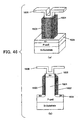
- FIGS. 46(a) and 46(b) show an SGT disclosed in the Patent Document 1, wherein FIG. 46(a) and FIG. 46(b) are, respectively, a bird's-eye view and a sectional view of the SGT.
- FIGS. 46(a) and 46(b) a structure of the SGT will be briefly described below.
- a pillar-shaped silicon layer 1601 is formed on a silicon substrate.
- a gate dielectric film 1602 is formed to surround the pillar-shaped silicon layer 1601, and a gate electrode 1603 is formed to surround the gate dielectric film 1602.
- a lower diffusion layer 1604 and an upper diffusion layer 1605 are formed underneath and in an upper portion of the pillar-shaped silicon layer 1601, respectively.
- the upper diffusion layer 1605 is connected to an interconnection layer 1606 via a contact.
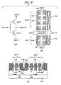
- FIGS. 47(a) to 47(c) show a CMOS inverter using an SGT, wherein FIG. 47(a), FIG. 47(b) and FIG. 47(c) are, respectively, an equivalent circuit of the CMOS inverter, a top plan view of the CMOS inverter, and a sectional view taken along the line B-B' in FIG. 47(b) .
- an N-well 2702 and a P-well 1703 are formed in an upper region of a Si substrate 1701.
- a pillar-shaped silicon layer 1705 constituting a PMOS transistor (PMOS pillar-shaped silicon layer 1705) and a pillar-shaped silicon layer 1706 constituting an NMOS transistor (NMOS pillar-shaped silicon layer 1706) are formed on a surface of the Si substrate, specifically on respective ones of the N-well region and the P-well region, and a gate 1708 is formed to surround the pillar-shaped silicon layers.
- a P + drain diffusion layer 1710 formed underneath the PMOS pillar-shaped silicon layer, and a N + drain diffusion layer 1712 formed underneath the NMOS pillar-shaped silicon layer is connected to an output terminal Vout 17.
- a source diffusion layer 1709 formed in an upper portion of the PMOS pillar-shaped silicon layer is connected to a power supply potential Vcc 17, and a source diffusion layer 1711 formed in an upper portion of the NMOS pillar-shaped silicon layer is connected to a ground potential GND 17. Further, the gate 1708 common to the PMOS and NMOS pillar-shaped silicon layers is connected to an input terminal Vin 17. In this manner, the CMOS inverter is formed.
- a pillar-shaped silicon layer As a prerequisite to enhancing a channel controllability by a gate in an SGT to sufficiently suppress short-channel effects, it is necessary to form a pillar-shaped silicon layer to have a sufficiently-small size relative to a gate length.
- a size of a pillar-shaped silicon layer can be reduced in a relatively easy manner, for example, by causing dimensional shrinking during dry etching for forming the pillar-shaped silicon layer, or by performing sacrificial oxidation after formation of the pillar-shaped silicon layer.
- a pillar-shaped silicon layer is formed to have a size less than a minimum fabrication size F, in order to sufficiently suppress the short-channel effects in an SGT.
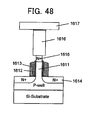
- FIG. 48 shows a structure of an SGT which comprises a pillar-shaped silicon layer 1611 having a size less than the minimum fabrication size F.
- a gate length is sufficiently large relative to the size of the pillar-shaped silicon layer 1611, so that the short-channel effects can be suppressed.
- a contact 1616 to be formed on a top of the pillar-shaped silicon layer is formed in a similar size to the minimum fabrication size F, so that it will become structurally larger than the pillar-shaped silicon layer 1611.
- the SGT structure illustrated in FIG. 48 has the following problems. Firstly, in terms of a need for forming a silicide layer on each of upper and lower sides of the pillar-shaped silicon layer to reduce a parasitic resistance in an SGT, a reduction in size of a pillar-shaped silicon layer causes difficulty in forming an adequate silicide on top of the pillar-shaped silicon layer due to the so-called "narrow width effect" on the silicide layer.
- an interface area between the silicide and an upper diffusion layer 1615 becomes smaller along with a reduction in diameter of the pillar-shaped silicon layer, so that an interface resistance between the silicide and the upper diffusion layer is increased to cause deterioration in transistor characteristics.
- the contact 1616 to be formed on top of the pillar-shaped silicon layer has to undergo overetching to an extent corresponding to a height dimension of the pillar-shaped silicon layer or more, as compared with the contact to be formed on the lower diffusion layer 1614.
- the contact to be formed on top of the pillar-shaped silicon layer is excessively overetched during etching for the contacts, so that a short-circuiting between the gate and the contact becomes more likely to occur.
- a MOS transistor which comprises: a pillar-shaped semiconductor layer; one of drain and source regions which is formed underneath the pillar-shaped semiconductor layer to serve as a first drain/source region; a gate electrode formed around a sidewall of the pillar-shaped semiconductor layer through a first dielectric film; an epitaxial semiconductor layer formed on top of an upper surface of the pillar-shaped semiconductor layer; and a remaining one of the drain and source regions which is formed so as to be at least partially in the epitaxial semiconductor layer to serve as a second drain/source region, wherein an area of an upper surface of the second drain/source region is greater than an area of the upper surface of the pillar-shaped semiconductor layer.
- the MOS transistor of the present invention further comprises a silicide layer formed on the upper surface of the second drain/source region.
- an interface area between the silicide layer and the second drain/source region is greater than the area of the upper surface of the pillar-shaped semiconductor layer.
- the epitaxial semiconductor layer consists of a silicon (Si) layer or a silicon carbide (SiC) layer formed by epitaxial growth, in cases where it is an n-type epitaxial semiconductor layer, or consists of a silicon (Si) layer or a silicon germanium (SiGe) layer formed by epitaxial growth, in cases where it is a p-type epitaxial semiconductor layer.
- the epitaxial semiconductor layers formed on tops of respective upper surfaces of the at least two pillar-shaped semiconductor layers are connected to each other to form a single common drain/source region.
- the epitaxial semiconductor layer is formed on top of the gate electrode through a second dielectric film.
- the above MOS transistor further comprises a contact formed on the silicide layer, wherein an area of the contact is less than an area of an upper surface of the silicide layer.
- the above MOS transistor further comprises at least one contact formed on the epitaxial semiconductor layers on tops of the upper surfaces of the at least two pillar-shaped semiconductor layers, wherein the number of the contacts is less than the number of the pillar-shaped semiconductor layers.
- the above MOS transistor further comprises at least one contact formed on the connected epitaxial semiconductor layers, wherein the at least one contact includes a contact formed on the connected epitaxial semiconductor layers at a position corresponding to a position between adjacent two of the at least two pillar-shaped semiconductor layers.
- the above MOS transistor further comprises a plurality of contacts at least one of which is formed on the connected epitaxial semiconductor layers, wherein an area of the at least one contact in cross-section parallel to a principal surface of the substrate is greater than that of each of the remaining contacts.
- a method of producing a semiconductor device having a MOS transistor comprises the steps of: providing a substrate having a plurality of pillar-shaped semiconductor layers formed thereover; forming one of drain and source regions underneath the pillar-shaped semiconductor layers to serve as a first drain/source region; forming a first dielectric film on a surface of the obtained product; forming a conductive film on the first dielectric film; etching back the first dielectric film and the conductive film to form each of the first dielectric film and the conductive film to have a height dimension equal to a gate length along a sidewall of each of the pillar-shaped semiconductor layers; removing a part of the conductive film and the first dielectric film by selective etching to form a gate electrode around the pillar-shaped semiconductor layers, and a gate line extending from the gate electrode; forming an epitaxial layer on top of an upper surface of at least one of the pillar-shaped semiconductor layers by epitaxial growth, in such a manner
- the method of the present invention further comprises the step of forming a silicide layer in a surface of the epitaxial layer.
- the epitaxial semiconductor layer consists of a silicon (Si) layer or a silicon carbide (SiC) layer formed by epitaxial growth, in cases where it is an n-type epitaxial semiconductor layer, or consists of a silicon (Si) layer or a silicon germanium (SiGe) layer formed by epitaxial growth, in cases where it is a p-type epitaxial semiconductor layer.
- conditions for film formation by epitaxial growth are adjusted in such a manner that only the epitaxial layers formed on tops of respective upper surfaces of the at least two of the pillar-shaped semiconductor layers constituting the MOS transistor are self-alignedly connected together to allow a single common drain/source region to be formed therein.
- the method of the present invention further comprises, as a pretreatment for the step of forming an epitaxial layer, the step of forming a second dielectric film for isolating between the gate electrode and the epitaxial semiconductor layer.
- the step of forming a second dielectric film includes the sub-steps of: forming a silicon nitride film or a laminated film comprised of a silicon nitride film and a silicon oxide film, on a surface of the product obtained from the step of removing a part of the conductive film and the first dielectric film; and etching back the silicon nitride film or the laminated film to cover a sidewall of each of the pillar-shaped semiconductor layers, a sidewall of the gate electrode and a sidewall of the gate line by the etched silicon nitride film or laminated film, while allowing the etched silicon nitride film or laminated film to remain on top of the gate electrode, and allowing the first drain/source region and an upper surface of each of the pillar-shaped semiconductor layers to be exposed.
- the step of providing a substrate having a plurality of pillar-shaped semiconductor layers formed thereover, and the step of forming one of drain and source regions underneath the pillar-shaped semiconductor layers to serve as a first drain/source region comprise the sub-steps of: forming a plurality of pillar-shaped semiconductor layers on a substrate; forming an element isolation region on the substrate; and forming one of drain and source regions on the substrate to serve as a first drain/source region.
- the step of providing a substrate having a plurality of pillar-shaped semiconductor layers formed thereover, and the step of forming one of drain and source regions underneath the pillar-shaped semiconductor layers to serve as a first drain/source region comprise the sub-steps of: forming a planar semiconductor layer, on a dielectric film on a substrate, and then forming a plurality of pillar-shaped semiconductor layers on the planar semiconductor layer substrate; isolating the planar semiconductor layer on an element-by-element basis; and forming one of drain and source regions in the isolated planar semiconductor layer to serve as a first drain/source region.
- the term "over a substrate” means a position on the substrate or a position located upwardly of the substrate through a certain layer formed on the substrate.
- the present invention makes it possible to reduce the narrow width effect on a silicide layer on top of a pillar-shaped silicon layer while reducing an interface resistance between the silicide and an upper diffusion layer, to improve transistor characteristics.
- the present invention also makes it possible to achieve a structure free of the occurrence of a short-circuiting between a contact and a gate.
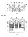
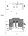
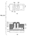
- FIG. 1(a) is a top plan view showing a transistor according to a first embodiment of the present invention
- FIG. 1(b) is a sectional view taken along the line A-A' in FIG. 1(a) .
- a silicon substrate 101 is isolated on an element-by-element basis by an element isolation region 102, and two pillar-shaped silicon layers (pillar-shaped semiconductor layers) 105a, 105b are formed on the silicon substrate.
- a gate dielectric film (first dielectric film) 107 and a gate electrode (108a, 108b) are formed around each of the pillar-shaped silicon layers (pillar-shaped semiconductor layers).
- a High-k film is used as the gate dielectric film (first dielectric film), and a metal film is used as the gate electrode.
- a silicon oxynitride film formed by oxidation may be used as the gate dielectric film (first dielectric film), and a polysilicon film may be used as the gate electrode.
- a lower N + diffusion layer (first drain/source diffusion region, i.e., one of drain and source diffusion regions) 103 is formed underneath the pillar-shaped silicon layers (pillar-shaped semiconductor layers), and a lower silicide layer 111a is formed on a surface of the lower N + diffusion layer (first drain/source diffusion region) 103, to reduce a parasitic resistance.
- An upper N + diffusion layer (second drain/source diffusion region, i.e., a remaining one of the drain and source diffusion regions) (109a, 109b) is formed on top of each of the pillar-shaped silicon layers (pillar-shaped semiconductor layers), in such a manner that an area of an upper surface thereof becomes greater than that of an upper surface of the pillar-shaped silicon layer.
- the upper N + diffusion layer (second drain/source diffusion region) (109a, 109b) having an upper surface with an area greater than that of the upper surface of the pillar-shaped silicon layer is comprised of an upper portion formed in an epitaxially-grown semiconductor epitaxial layer, and a lower portion formed in an upper portion of the pillar-shaped silicon layer.
- the upper N + diffusion layer (second drain/source diffusion region) (109a, 109b) may be formed only in a part or an entirety of the semiconductor epitaxial layer.
- the semiconductor epitaxial layer is electrically isolated from the gate electrode (108a, 108b) by a second dielectric film 112, such as a silicon nitride film or a laminated film comprised of a silicon nitride film and a silicon oxide film, interposed therebetween.
- An upper silicide layer (111b, 111c) is formed on the upper N + diffusion layer (second drain/source diffusion region) (109a, 109b).
- the upper silicide layer is formed on the epitaxial silicon layer (semiconductor epitaxial layer) having a diameter greater than that of the pillar-shaped silicon layer (pillar-shaped semiconductor layer).
- the narrow width effect on the upper silicide layer can be reduced.
- an interface area between the upper silicide layer and the upper N + diffusion layer can be set largely, so that an interface resistance between the upper silicide layer and the upper N + diffusion layer can be reduced.
- the upper silicide layer (111b, 111c) may be formed on an upper surface of the upper N + diffusion layer (second drain/source diffusion region) to have a diameter greater than that of a contact (115, 116) to be formed on an upper side of the pillar-shaped silicon layer (pillar-shaped semiconductor layer).
- the contact (115, 116) formed on the upper side of the pillar-shaped silicon layer (pillar-shaped semiconductor layer) is connected to one of drain and source terminals through an interconnection layer 120.
- a contact 118 formed on a lower side of the pillar-shaped silicon layer (pillar-shaped semiconductor layer) is connected to a remaining one of the drain and source terminals through an interconnection layer 122, and a contact 117 formed on a gate line 108 extending from the gate electrode is connected to a gate terminal through an interconnection layer 121.
- a thickness of a film to be epitaxially grown can be adjusted in such a manner that the silicon epitaxial layers (semiconductor epitaxial layers on respective ones of the adjacent pillar-shaped semiconductor layers are self-alignedly connected together.
- an interface area between an upper silicide layer 211b on an upper side of the pillar-shaped silicon layers (pillar-shaped semiconductor layers) and an integral set of upper N + diffusion layers (second drain/source diffusion regions) 209a, 209b becomes larger, so that an interface resistance between the an upper silicide layer and the integral set of upper N + diffusion layers (second drain/source diffusion regions) can be further reduced.
- an area of the upper silicide layer on the upper side of the pillar-shaped silicon layers (pillar-shaped semiconductor layers) becomes larger, so that the narrow width effect on the upper silicide layer can be significantly reduced to facilitate adequate formation of the upper silicide layer.
- an upper side of the pillar-shaped semiconductor layers may be connected to an interconnection layer via a less number of contacts than the number of the pillar-shaped semiconductor layers.
- a contact 415 may be formed on an integral set of upper N + diffusion layers (second drain/source diffusion regions) 409a, 409b at a position corresponding to a position between adjacent pillar-shaped silicon layers (pillar-shaped semiconductor layers).
- an axis of the contact 415 may be located to intersect with a line segment connecting respective axes of the adjacent pillar-shaped silicon layers (pillar-shaped semiconductor layers) or may be located in a region between the axes of the adjacent pillar-shaped silicon layers (pillar-shaped semiconductor layers).
- a contact 515 having an area greater than that of other contact (517, 518) in cross-section parallel to a principal surface of a substrate may be formed on an upper side of a plurality of pillar-shaped silicon layers (pillar-shaped semiconductor layers), in a number less than the number of the pillar-shaped semiconductor layers. This makes it possible to reduce a resistance of a contact, and stably form a contact.
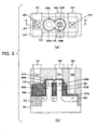
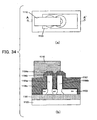
- FIGS. 6(a) to 20(b) one example of a production method for the transistor illustrated in FIGS. 2(a) and 2(b) will be described below.
- the figure suffixed with (a) is a top plan view
- the figure suffixed with (b) is a sectional view taken along the line A-A' in the figure suffixed with (a).
- two pillar-shaped silicon layers (pillar-shaped semiconductor layers) 205a, 205b each having a hard mask layer 204a, such as a silicon nitride film, on top thereof, are formed on a substrate 201 by lithography and etching.
- an element isolation 202 is formed in the substrate.
- the element isolation is formed by etching the substrate to form a trench pattern, filling an oxide film in the trench pattern through chemical vapor deposition (CVD) or silica coating or the like, and removing an excess part of the oxide film on the substrate through dry etching or wet etching.
- CVD chemical vapor deposition
- silica coating or the like removing an excess part of the oxide film on the substrate through dry etching or wet etching.
- a lower N + diffusion layer 203 is formed underneath the pillar-shaped silicon layers (pillar-shaped semiconductor layers) by ion implantation or the like.
- the pillar-shaped silicon layer (pillar-shaped semiconductor layer) (205a, 205b) is kept from impurity implantation by the hard mask layer 204a on top of the pillar-shaped silicon layer (pillar-shaped semiconductor layer).
- a gate dielectric film (first dielectric film) 207 and a gate conductive film 208c are formed.
- the gate dielectric film (first dielectric film) 207 is formed of an oxide film, a High-k film or the like.
- the gate conductive film 208c is formed of a polysilicon film, a metal film or the like.
- the gate conductive film 208c is flattened by chemical mechanical polishing (CMP) or the like.
- the gate dielectric film (first dielectric film) 207 and the gate conductive film 208c are etched back to allow a height dimension of each of the gate dielectric film (first dielectric film) 207 and the gate conductive film 208c along a sidewall of the pillar-shaped silicon layer (pillar-shaped semiconductor layer) (205a, 205b) to be set to a desired gate length.
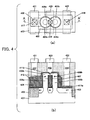
- a nitride film or the like is formed and then etched back to form a sidewall spacer 204b.
- a gate line pattern is formed using a resist 210 by lithography or the like.
- the gate conductive film 208c and the gate dielectric film (first dielectric film) 207 are selectively etched by anisotropic etching or the like, using the resist 210 as a mask, to integrally form a gate electrode (208a, 208b) around the pillar-shaped silicon layer (pillar-shaped semiconductor layer) (205a, 205b) and a gate line 208 extending from the gate electrode (208a, 208b), . Subsequently, the resist 210 is removed.
- the hard mask layer 204a and the sidewall spacer 204b are removed by wet etching or the like.
- a dielectric film such as a nitride film or a laminated film comprised of a nitride film and an oxide film, is formed, and then etched back to form a second dielectric film 212.
- silicon or the like is selectively epitaxially grown on top of an upper surface of each of the pillar-shaped silicon layer (pillar-shaped semiconductor layer) and on the lower N + diffusion layer 203 to form an upper epitaxial silicon layer (semiconductor epitaxial layer) 210b and a lower epitaxial silicon layer, in such a manner that epitaxial layers formed on tops of respective upper surfaces of the pillar-shaped silicon layers (pillar-shaped semiconductor layers) arranged adjacent to each other with a given distance or less therebetween are self-alignedly connected together.
- the upper epitaxial silicon layer may be formed to have a diameter greater than that of a contact to be formed on an upper side of the pillar-shaped silicon layer (pillar-shaped semiconductor layer) in a subsequent step. This makes it possible to provide a structure free of a short-circuiting between the contact and the gate electrode.
- an upper N + diffusion layer (209a, 209b) is formed in the upper epitaxial silicon layer (semiconductor epitaxial layer) 210b and an upper portion of the pillar-shaped silicon layer (pillar-shaped semiconductor layer) (205a, 205b) by ion implantation or the like.
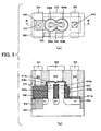
- a region to be formed as the upper N + diffusion layer (second drain/source diffusion region) may be a part or an entirety of the upper epitaxial silicon layer (semiconductor epitaxial layer) 210b.
- a metal such as Co or Ni
- a heat treatment is performed to selectively silicide respective upper surfaces of the lower epitaxial silicon layer on the lower N + diffusion layer (first drain/source diffusion region) 203 and the integral set of upper N + diffusion layers (second drain/source diffusion regions) to form a lower silicide layer 211a and an upper silicide layer 211b.
- the upper silicide layer 211b is formed to have a size greater than that of the pillar-shaped silicon layer (pillar-shaped semiconductor layer), so that the narrow width effect on the upper silicide layer can be suppressed.
- the entire surface of the epitaxial silicon layer may be silicided.
- an interface area between the upper silicide layer 211b and the integral set of upper N + diffusion layers (second drain/source diffusion regions) 209a, 209b is increased, so that an interface resistance therebetween can be reduced to reduce a source/drain parasitic resistance.
- a silicon oxide film is formed to serve as an interlayer film, and then a contact (215 to 218) is formed.
- the epitaxial silicon layer semiconductor epitaxial layer
- the epitaxial silicon layer is formed to allow the contact (215, 216) on an upper side of the pillar-shaped silicon layer (pillar-shaped semiconductor layer) to be entirely formed on the upper silicide layer 211b, as shown in FIGS. 20(a) and 20(b) . This makes it possible to provide a structure free of a short-circuiting between the contact and the gate electrode.
- the first embodiment shows one example where an epitaxial silicon layer (semiconductor epitaxial layer) is formed.
- an epitaxial silicon carbide (SiC) layer may be formed for an NMOS transistor, and an epitaxial silicon germanium (SiGe) layer may be formed for a PMOS transistor.
- SiC silicon carbide
- SiGe silicon germanium
- a stress can be applied to a channel region to enhance carrier mobility.
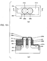
- FIG. 21(a) is a top plan view showing a transistor according to the second embodiment
- FIG. 21(b) is a sectional view taken along the line A-A' in FIG. 21(a) .
- FIGS. 21(a) and 21(b) a structure of the transistor according to the second embodiment will be described below.
- a silicon substrate 601 is isolated on an element-by-element basis by an element isolation 602.
- a High-k film is used as the gate dielectric film (first dielectric film), and a metal film is used as the gate electrode.
- a silicon oxynitride film formed by oxidation may be used as the gate dielectric film (first dielectric film), and a polysilicon film may be used as the gate electrode.
- a lower N + diffusion layer (first drain/source diffusion region, i.e., one of drain and source diffusion regions) 603 is formed underneath the pillar-shaped silicon layers (pillar-shaped semiconductor layers), and a lower silicide layer 611a is formed on a surface of the lower N + diffusion layer (first drain/source diffusion region) 603, to reduce a parasitic resistance.
- An upper N + diffusion layer (second drain/source diffusion region, i.e., a remaining one of the drain and source diffusion regions) (609a to 609d) is formed on top of each of the pillar-shaped silicon layers (pillar-shaped semiconductor layers), in such a manner that an area of an upper surface thereof becomes greater than that of an upper surface of the pillar-shaped silicon layer.
- the upper N + diffusion layer (second drain/source diffusion region) having an upper surface with an area greater than that of the upper surface of the pillar-shaped silicon layer is comprised of an upper portion formed in an epitaxially-grown semiconductor epitaxial layer, and a lower portion formed in an upper portion of the pillar-shaped silicon layer.
- the upper N + diffusion layer may be formed only in a part or an entirety of the semiconductor epitaxial layer.
- the semiconductor epitaxial layer is electrically isolated from the gate electrode (608a to 608d) by a second dielectric film 612, such as a silicon nitride film or a laminated film comprised of a silicon nitride film and a silicon oxide film, interposed therebetween.
- the two pillar-shaped silicon layers (pillar-shaped semiconductor layers) 605a, 605b constituting the first transistor are arranged adjacent to each other, so that epitaxial silicon layers (semiconductor epitaxial layers) to be formed on tops of respective upper surfaces of the adjacent pillar-shaped silicon layers (pillar-shaped semiconductor layers) are self-alignedly connected together.
- the two pillar-shaped silicon layers (pillar-shaped semiconductor layers) 605c, 605d constituting the second transistor are also arranged adjacent to each other, so that epitaxial silicon layers (semiconductor epitaxial layers) to be formed on tops of respective upper surfaces of the adjacent pillar-shaped silicon layers (pillar-shaped semiconductor layers) are self-alignedly connected together in the same manner.
- the two pillar-shaped silicon layers (pillar-shaped semiconductor layers) 605b, 605c each constituting a different transistor are arranged with a distance greater than a given value therebetween, so that epitaxial silicon layers (semiconductor epitaxial layers) to be formed thereon are separated from each other.
- Two upper silicide layers 611b, 611c are formed, respectively, on the integral set of upper N + diffusion layers (second drain/source diffusion regions) 609a, 609b and the integral set of upper N + diffusion layers (second drain/source diffusion regions) 609c, 609d.
- Each of the upper silicide layers is formed on the connected epitaxial silicon layers (semiconductor epitaxial layers) each having a diameter greater than that of the pillar-shaped silicon layer (pillar-shaped semiconductor layer). Thus, the narrow width effect on the upper silicide layer can be reduced.
- an interface area between the upper silicide layer and the integral set of upper N+ diffusion layers (609a, 609b; 609c, 609d) can be set largely, so that an interface resistance between the upper silicide layer and the integral set of upper N + diffusion layers can be reduced.
- the upper silicide layer (611b, 611c) may be formed in an upper surface of the integral set of the upper N + diffusion layers (second drain/source diffusion regions) to have a diameter greater than a total diameter of two contacts (615a, 615b; 616a, 616b) to be formed on an upper side of the adjacent pillar-shaped silicon layers (pillar-shaped semiconductor layers).
- the two contacts 615a, 615b formed on the upper side of the pillar-shaped silicon layers (pillar-shaped semiconductor layers) constituting the first transistor are connected to one of drain and source terminals through an interconnection layer 620a, and the two contacts 616a, 616b formed on the upper side of the pillar-shaped silicon layers (pillar-shaped semiconductor layers) constituting the second transistor are connected to a remaining one of the drain and source terminals through an interconnection layer 620b. Further, the first transistor and the second transistor are connected in series through the lower N + diffusion layer (first drain/source diffusion region) 603.
- a contact 617 formed on a gate line 608 extending from the gate electrode is connected to a gate terminal through an interconnection layer 621.
- an upper side of the pillar-shaped semiconductor layers may be connected to an interconnection layer via a less number of contacts than the number of the pillar-shaped semiconductor layers.
- a contact (715, 716) may be formed on an integral set of upper N + diffusion layers (second drain/source diffusion regions) 409a, 409b at a position corresponding to a position between adjacent pillar-shaped silicon layers (pillar-shaped semiconductor layers).
- an axis of the contact (715, 716) may be located to intersect with a line segment connecting respective axes of the adjacent pillar-shaped silicon layers (pillar-shaped semiconductor layers) or may be located in a region between the axes of the adjacent pillar-shaped silicon layers (pillar-shaped semiconductor layers).
- a contact having an area greater than that of other contact in cross-section parallel to a principal surface of a substrate may be formed on an upper side of a plurality of pillar-shaped silicon layers (pillar-shaped semiconductor layers), in a number less than the number of the pillar-shaped semiconductor layers. This makes it possible to reduce a resistance of a contact, and stably form a contact.
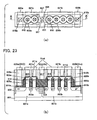
- FIG. 23(a) is a top plan view showing a CMOS inverter according to the third embodiment
- FIG. 23(b) is a sectional view taken along the line A-A' in FIG. 23(a) .
- an interconnection layer 820a connected to an NMOS transistor is connected to GND
- an interconnection layer 820b connected to a PMOS transistor is connected to Vcc.
- An input signal Vin is input into a gate interconnection layer 808 from an interconnection layer 822, and two interconnection lines 821a, 821b connected from respective upper sides of the NMOS and PMOS transistors are connected to each other through an interconnection layer to output an output signal Vout therefrom. In this manner, a CMOS inverter is formed.
- a silicon substrate 801 is isolated on an element-by-element basis by an element isolation 802.
- a gate dielectric film (first dielectric film) 807 and a gate electrode (808a, 808b) are formed around each of the pillar-shaped silicon layers (pillar-shaped semiconductor layers).
- a High-k film is used as the gate dielectric film (first dielectric film)
- a metal film is used as the gate electrode.
- a silicon oxynitride film formed by oxidation may be used as the gate dielectric film (first dielectric film), and a polysilicon film may be used as the gate electrode.
- a lower N + diffusion layer (first drain/source diffusion region, i.e., one of drain and source diffusion regions) 803a surrounded by a P-well 801a is formed underneath the NMOS pillar-shaped silicon layers (NMOS pillar-shaped semiconductor layers) 805a, and a lower P + diffusion layer (first drain/source diffusion region) 803b surrounded by an N-well 801b is formed underneath the PMOS pillar-shaped silicon layers (PMOS pillar-shaped semiconductor layers) 805b.
- a lower silicide layer (811a, 811b) is formed on a surface of each of the lower N + and P+ diffusion layers (first drain/source diffusion regions) to reduce a parasitic resistance.
- An upper N + diffusion layer (second drain/source diffusion region, i.e., a remaining one of the drain and source diffusion regions) 809a is formed on top of each of the NMOS pillar-shaped silicon layers (NMOS pillar-shaped semiconductor layers) 805a in such a manner that an area of an upper surface thereof becomes greater than that of an upper surface of the NMOS pillar-shaped silicon layer.
- An upper P + diffusion layer (second drain/source diffusion region) 809b is formed on top of each the PMOS pillar-shaped silicon layers (PMOS pillar-shaped semiconductor layers) 805b in such a manner that an area of an upper surface thereof becomes greater than that of an upper surface of the PMOS pillar-shaped silicon layer.
- the upper diffusion layer having an upper surface with an area greater than that of the upper surface of the pillar-shaped silicon layer is comprised of an upper portion formed in an epitaxially-grown semiconductor epitaxial layer, and a lower portion formed in an upper portion of the pillar-shaped silicon layer.
- the upper diffusion layer may be formed only in a part or an entirety of the semiconductor epitaxial layer.
- the semiconductor epitaxial layer is electrically isolated from the gate electrode (808a, 808b) by a second dielectric film 812, such as a silicon nitride film or a laminated film comprised of a silicon nitride film and a silicon oxide film, interposed therebetween.
- the two NMOS pillar-shaped silicon layers (NMOS pillar-shaped semiconductor layers) 805a are arranged adjacent to each other, so that epitaxial silicon layers (semiconductor epitaxial layers) to be formed on tops of respective upper surfaces of the NMOS pillar-shaped silicon layers (NMOS pillar-shaped semiconductor layers) are self-alignedly connected together.
- the four PMOS pillar-shaped silicon layers (PMOS pillar-shaped semiconductor layers) 805b are also arranged adjacent to each other, so that epitaxial silicon layers (semiconductor epitaxial layers) to be formed on tops of respective upper surfaces of the PMOS pillar-shaped silicon layers (PMOS pillar-shaped semiconductor layers) are self-alignedly connected together in the same manner.
- Two upper silicide layers 811c, 811d are formed, respectively, on the integral set of upper N + diffusion layers 809a and the integral set of upper P + diffusion layers (second drain/source diffusion regions) 809b.
- Each of the upper silicide layers is formed on the connected epitaxial silicon layers (semiconductor epitaxial layers) each having a diameter greater than that of the pillar-shaped silicon layer (pillar-shaped semiconductor layer).
- the narrow width effect on the upper silicide layer can be reduced.
- an interface area between the upper silicide layer and the integral set of upper diffusion layers (809a, 809b) can be set largely, so that an interface resistance between the upper silicide layer and the integral set of upper diffusion layers can be reduced.
- the upper silicide layer (811c, 811d) may be formed in an upper surface of the integral set of the upper diffusion layers (second drain/source diffusion regions) to have a diameter greater than a total diameter of a plurality of contacts (815, 816) to be formed on an upper side of the adjacent pillar-shaped silicon layers (pillar-shaped semiconductor layers). This makes it possible to prevent a short-circuiting between the contact and the gate electrode even if the contact undergoes overetching during etching for contacts. As shown in FIGS.
- an upper side of the pillar-shaped semiconductor layers may be connected to an interconnection layer via a less number of contacts than the number of the pillar-shaped semiconductor layers.
- a contact 915 may be formed on an integral set of upper N + diffusion layers (second drain/source diffusion regions) 909a at a position corresponding to a position between adjacent pillar-shaped silicon layers (pillar-shaped semiconductor layers).
- an axis of the contact 915 may be located to intersect with a line segment connecting respective axes of the adjacent pillar-shaped silicon layers (pillar-shaped semiconductor layers) or may be located in a region between the axes of the adjacent pillar-shaped silicon layers (pillar-shaped semiconductor layers).
- the number of contacts can be reduced by this arrangement or an arrangement in a PMOS transistor illustrated in FIGS. 24(a) and 24(b) . This makes it possible to largely set a space between adjacent ones of a plurality of interconnection lines 920a, 920b, 921a, 921b, 922 so as to facilitate interconnection layout.
- a contact having an area greater than that of other contact in cross-section parallel to a principal surface of a substrate may be formed on an upper side of a plurality of pillar-shaped silicon layers (pillar-shaped semiconductor layers), in a number less than the number of the pillar-shaped semiconductor layers. This makes it possible to reduce a resistance of a contact, and stably form a contact.
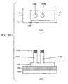
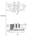
- FIG. 25(a) is a top plan view showing a transistor using an SOI substrate according to a fourth embodiment of the present invention
- FIG. 25(b) is a sectional view taken along the line A-A' in FIG. 25(a) .
- an SOI transistor according to the fourth embodiment will be described below.
- a silicon layer 1002 on an SOI (silicon on insulator) substrate is isolated on an element-by-element basis, and two pillar-shaped silicon layers (pillar-shaped semiconductor layers) 1005a, 1005b are formed on the silicon layer 1002.
- a gate dielectric film (first dielectric film) 1007 and a gate electrode (1008a, 1008b) are formed around each of the pillar-shaped silicon layers (pillar-shaped semiconductor layers).
- a High-k film is used as the gate dielectric film (first dielectric film)
- a metal film is used as the gate electrode.
- a silicon oxynitride film formed by oxidation may be used as the gate dielectric film (first dielectric film), and a polysilicon film may be used as the gate electrode.
- a lower N + diffusion layer (first drain/source diffusion region, i.e., one of drain and source diffusion regions) 1003 is formed underneath the pillar-shaped silicon layers (pillar-shaped semiconductor layers), and a lower silicide layer 1011a is formed on a surface of the lower N + diffusion layer (first drain/source diffusion region) 1003, to reduce a parasitic resistance.
- An upper N + diffusion layer (second drain/source diffusion region, i.e., a remaining one of the drain and source diffusion regions) (1009a, 1009b) is formed on top of each of the pillar-shaped silicon layers (pillar-shaped semiconductor layers), in such a manner that an area of an upper surface thereof becomes greater than that of an upper surface of the pillar-shaped silicon layer.
- the upper N + diffusion layer (second drain/source diffusion region) having an upper surface with an area greater than that of the upper surface of the pillar-shaped silicon layer is comprised of an upper portion formed in an epitaxially-grown semiconductor epitaxial layer, and a lower portion formed in an upper portion of the pillar-shaped silicon layer.
- the upper N + diffusion layer (second drain/source diffusion region) may be formed only in a part or an entirety of the semiconductor epitaxial layer.
- the semiconductor epitaxial layer is electrically isolated from the gate electrode (1008a, 1008b) by a second dielectric film 1012, such as a silicon nitride film or a laminated film comprised of a silicon nitride film and a silicon oxide film, interposed therebetween.
- An upper silicide layer (1011b, 1011c) is formed on the upper N + diffusion layer (second drain/source diffusion region) (1009a, 1009b).
- the upper silicide layer is formed on the epitaxial silicon layer (semiconductor epitaxial layer) having a diameter greater than that of the pillar-shaped silicon layer (pillar-shaped semiconductor layer).
- the narrow width effect on the upper silicide layer can be reduced.
- an interface area between the upper silicide layer and the upper N + diffusion layer can be set largely, so that an interface resistance between the upper silicide layer and the upper N + diffusion layer can be reduced.
- the upper silicide layer (1011b, 1011c) may be formed in an upper surface of the upper N + diffusion layer (second drain/source diffusion region) to have a diameter greater than that of a contact (1015, 1016) to be formed on an upper side of the pillar-shaped silicon layer (pillar-shaped semiconductor layer). This makes it possible to prevent a short-circuiting between the contact and the gate electrode even if the contact undergoes overetching during etching for contacts.
- the contact (1015, 1016) formed on the upper side of the pillar-shaped silicon layer (pillar-shaped semiconductor layer) is connected to one of drain and source terminals through an interconnection layer 1020.
- a contact 1018 formed on a lower side of the pillar-shaped silicon layer (pillar-shaped semiconductor layer) is connected to a remaining one of the drain and source terminals through an interconnection layer 1022, and a contact 1017 formed on a gate line 1008 extending from the gate electrode is connected to a gate terminal through an interconnection layer 1021.
- a thickness of a film to be epitaxially grown can be adjusted in such a manner that the epitaxial silicon layers (semiconductor epitaxial layers) on respective ones of the adjacent pillar-shaped semiconductor layers are self-alignedly connected together.
- an interface area between an upper silicide layer 1111b on an upper side of the pillar-shaped silicon layers (pillar-shaped semiconductor layers) and an integral set of upper N + diffusion layers (second drain/source diffusion regions) 1109a, 1109b formed in the connected semiconductor epitaxial layers becomes larger, so that an interface resistance between the an upper silicide layer and the integral set of upper N + diffusion layers (second drain/source diffusion regions) can be further reduced.
- an area of the upper silicide layer 1111a on the upper side of the pillar-shaped silicon layers (pillar-shaped semiconductor layers) becomes larger, so that the narrow width effect on the upper silicide layer can be significantly reduced to facilitate adequate formation of the upper silicide layer.
- an upper side of the pillar-shaped semiconductor layers may be connected to an interconnection layer via a less number of contacts than the number of the pillar-shaped semiconductor layers, as described in connection with FIGS. 3(a) and 3(b) .
- a contact may be formed on an integral set of upper N + diffusion layers (second drain/source diffusion regions) at a position corresponding to a position between adjacent pillar-shaped silicon layers (pillar-shaped semiconductor layers), as described in connection with FIGS. 4(a) and 4(b) .
- an axis of the contact may be located to intersect with a line segment connecting respective axes of the adjacent pillar-shaped silicon layers (pillar-shaped semiconductor layers) or may be located in a region between the axes of the adjacent pillar-shaped silicon layers (pillar-shaped semiconductor layers).
- a contact having an area greater than that of other contact in cross-section parallel to a principal surface of a substrate may be formed on an upper side of a plurality of pillar-shaped silicon layers (pillar-shaped semiconductor layers), in a number less than the number of the pillar-shaped semiconductor layers, as described in connection with FIGS. 5(a) and 5(b) . This makes it possible to reduce a resistance of a contact, and stably form a contact.
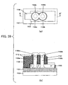
- FIGS. 27(a) to 41(b) one example of a production method for the transistor illustrated in FIGS. 26(a) and 26(b) will be described below.
- the figure suffixed with (a) is a top plan view
- the figure suffixed with (b) is a sectional view taken along the line A-A' in the figure suffixed with (a).
- two pillar-shaped silicon layers (pillar-shaped semiconductor layers) 1105a, 1105b having a hard mask layer 1104a, such as a silicon nitride film, on top thereof, are formed on a silicon layer 1102 on an SOI substrateby lithography and etching.
- the silicon layer 1102 on the SOI substrate is isolated on an element-by-element basis.
- a lower N + diffusion layer 1103 is formed underneath the pillar-shaped silicon layers (pillar-shaped semiconductor layers) by ion implantation or the like.
- the pillar-shaped silicon layer (pillar-shaped semiconductor layer) (1105a, 1105b) is kept from impurity implantation by the hard mask layer 1104a on top of the pillar-shaped silicon layer (pillar-shaped semiconductor layer).
- a gate dielectric film (first dielectric film) 1107 and a gate conductive film 1108c are formed.
- the gate dielectric film (first dielectric film) 1107 is formed of an oxide film, a High-k film or the like.
- the gate conductive film 1108c is formed of a polysilicon film, a metal film or the like.
- the gate conductive film 1108c is flattened by chemical mechanical polishing (CMP) or the like.
- the gate dielectric film (first dielectric film) 1107 and the gate conductive film 1108c are etched back to allow a height dimension of each of the gate dielectric film (first dielectric film) 1107 and the gate conductive film 1108c along a sidewall of the pillar-shaped silicon layer (pillar-shaped semiconductor layer) (1105a, 1105b) to be set to a desired gate length.
- a nitride film or the like is formed and then etched back to form a sidewall spacer 1104b.
- a gate line pattern is formed using a resist 1110 by lithography or the like.
- the gate conductive film 1108c and the gate dielectric film (first dielectric film) 1107 are selectively etched by anisotropic etching or the like, using the resist 1110 as a mask, to integrally form a gate electrode (1108a, 1108b) around the pillar-shaped silicon layer (pillar-shaped semiconductor layer) (1105a, 1105b) and a gate line 1108 extending from the gate electrode (1108a, 1108b). Subsequently, the resist 1110 is removed.
- the hard mask layer 1104a and the sidewall spacer 1104b are removed by wet etching or the like.
- a dielectric film such as a nitride film or a laminated film comprised of a nitride film and an oxide film, is formed, and then etched back to form a second dielectric film 1112.
- silicon or the like is selectively epitaxially grown on top of an upper surface of each of the pillar-shaped silicon layer (pillar-shaped semiconductor layer) and on the lower N + diffusion layer 1103 to form an upper epitaxial silicon layer (semiconductor epitaxial layer) 1110b and a lower epitaxial silicon layer, in such a manner that epitaxial layers formed on tops of respective upper surfaces of the pillar-shaped silicon layers (pillar-shaped semiconductor layers) arranged adjacent to each other with a given distance or less therebetween are self-alignedly connected together.
- the upper epitaxial silicon layer may be formed to have a diameter greater than that of a contact to be formed on an upper side of the pillar-shaped silicon layer (pillar-shaped semiconductor layer) in a subsequent step. This makes it possible to provide a structure free of a short-circuiting between the contact and the gate electrode.
- an upper N + diffusion layer (second drain/source diffusion region) (1109a, 1109b) is formed in the upper epitaxial silicon layer (semiconductor epitaxial layer) 1110b and an upper portion of the pillar-shaped silicon layer (pillar-shaped semiconductor layer) (1105a, 1105b) by ion implantation or the like.
- a metal such as Co or Ni
- a heat treatment is performed to selectively silicide respective upper surfaces of the lower epitaxial silicon layer on the lower N + diffusion layer (first drain/source diffusion region) 1103 and the integral set of upper N + diffusion layers (second drain/source diffusion regions) 1109a, 1109b to form a lower silicide layer 1111a and an upper silicide layer 1111b.
- the upper silicide layer 1111b is formed to have a size greater than that of the pillar-shaped silicon layer (pillar-shaped semiconductor layer), so that the narrow width effect on the upper silicide layer can be suppressed.
- the entire surface of the epitaxial silicon layer may be silicided.
- an interface area between the upper silicide layer 1111b and the integral set of upper N + diffusion layers (second drain/source diffusion regions) 1109a, 1109b is increased, so that an interface resistance therebetween can be reduced to reduce a source/drain parasitic resistance.
- a silicon oxide film is formed to serve as an interlayer film, and then a contact (1115 to 1118) is formed.
- the epitaxial silicon layer semiconductor epitaxial layer
- the epitaxial silicon layer is formed to allow the contact (1115, 1116) on an upper side of the pillar-shaped silicon layer (pillar-shaped semiconductor layer) to be entirely formed on the upper silicide layer 1111b, as shown in FIGS. 41(a) and 41(b) . This makes it possible to provide a structure free of a short-circuiting between the contact and the gate electrode.
- the fourth embodiment shows one example where an epitaxial silicon layer (semiconductor epitaxial layer) is formed.
- an epitaxial silicon carbide (SiC) layer may be formed for an NMOS transistor, and an epitaxial silicon germanium (SiGe) layer may be formed for a PMOS transistor.
- SiC silicon carbide
- SiGe silicon germanium
- a stress can be applied to a channel region to enhance carrier mobility.
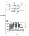
- FIG. 42(a) is a top plan view showing a transistor according to the fifth embodiment
- FIG. 42(b) is a sectional view taken along the line A-A' in FIG. 42(a) .
- FIGS. 42(a) and 42(b) a structure of the transistor according to the fifth embodiment will be described below.
- a silicon layer 1202 on an SOI substrate is isolated on an element-by-element basis.
- a High-k film is used as the gate dielectric film (first dielectric film), and a metal film is used as the gate electrode.
- a silicon oxynitride film formed by oxidation may be used as the gate dielectric film (first dielectric film), and a polysilicon film may be used as the gate electrode.
- a lower N + diffusion layer (first drain/source diffusion region, i.e., one of drain and source diffusion regions) 1203 is formed underneath the pillar-shaped silicon layers (pillar-shaped semiconductor layers), and a lower silicide layer 1211a is formed on a surface of the lower N + diffusion layer (first drain/source diffusion region) 1203, to reduce a parasitic resistance.
- An upper N + diffusion layer (second drain/source diffusion region, i.e., a remaining one of the drain and source diffusion regions) (1209a to 1209d) is formed on top of each of the pillar-shaped silicon layers (pillar-shaped semiconductor layers), in such a manner that an area of an upper surface thereof becomes greater than that of an upper surface of the pillar-shaped silicon layer.
- the upper N + diffusion layer (second drain/source diffusion region) having an upper surface with an area greater than that of the upper surface of the pillar-shaped silicon layer is comprised of an upper portion formed in an epitaxially-grown semiconductor epitaxial layer, and a lower portion formed in an upper portion of the pillar-shaped silicon layer.
- the upper N + diffusion layer may be formed only in a part or an entirety of the semiconductor epitaxial layer.
- the semiconductor epitaxial layer is electrically isolated from the gate electrode 1208a to 1208d by a second dielectric film 1212, such as a silicon nitride film or a laminated film comprised of a silicon nitride film and a silicon oxide film, interposed therebetween.
- the two pillar-shaped silicon layers (pillar-shaped semiconductor layers) 1205a, 1205b constituting the first transistor are arranged adjacent to each other, so that epitaxial silicon layers (semiconductor epitaxial layers) to be formed on tops of respective upper surfaces of the adjacent pillar-shaped silicon layers (pillar-shaped semiconductor layers) are self-alignedly connected together.
- the two pillar-shaped silicon layers (pillar-shaped semiconductor layers) 1205c, 1205d constituting the second transistor are also arranged adjacent to each other, so that epitaxial silicon layers (semiconductor epitaxial layers) to be formed on tops of respective upper surfaces of the adjacent pillar-shaped silicon layers (pillar-shaped semiconductor layers) are self-alignedly connected together in the same manner.
- the two pillar-shaped silicon layers (pillar-shaped semiconductor layers) 1205b, 1205c each constituting a different transistor are arranged with a distance greater than a given value therebetween, so that epitaxial silicon layers (semiconductor epitaxial layers) to be formed thereon are separated from each other.
- Two upper silicide layers 1211b, 1211c are formed, respectively, on the integral set of upper N + diffusion layers (second drain/source diffusion regions) 1209a, 1209b and the integral set of upper N + diffusion layers (second drain/source diffusion regions) 1209c, 1209d.
- Each of the upper silicide layers is formed on the connected epitaxial silicon layers (semiconductor epitaxial layers) each having a diameter greater than that of the pillar-shaped silicon layer (pillar-shaped semiconductor layer). Thus, the narrow width effect on the upper silicide layer can be reduced.
- an interface area between the upper silicide layer and the integral set of upper N+ diffusion layers (1209a to 1209d) can be set largely, so that an interface resistance between the upper silicide layer and the integral set of upper N + diffusion layers can be reduced.
- the upper silicide layer (1211b, 1211c) may be formed in an upper surface of the integral set of the upper N + diffusion layers (second drain/source diffusion regions) to have a diameter greater than a total diameter of two contacts (1215a, 1215b; 1216a, 1216b) to be formed on an upper side of the adjacent pillar-shaped silicon layers (pillar-shaped semiconductor layers).
- the two contacts 1215a, 1215b formed on the upper side of the pillar-shaped silicon layers (pillar-shaped semiconductor layers) constituting the first transistor are connected to one of drain and source terminals through an interconnection layer 1220a, and the two contacts 1216a, 1216b formed on the upper side of the pillar-shaped silicon layers (pillar-shaped semiconductor layers) constituting the second transistor are connected to a remaining one of the drain and source terminals through an interconnection layer 1220b. Further, the first transistor and the second transistor are connected in series through the lower N + diffusion layer (first drain/source diffusion region) 1203.
- a contact 1217 formed on a gate line 1208 extending from the gate electrode is connected to a gate terminal through an interconnection layer 1221.
- an upper side of the pillar-shaped semiconductor layers may be connected to an interconnection layer via a less number of contacts than the number of the pillar-shaped semiconductor layers, as described in connection with FIGS. 22(a) and 22(b) .
- a contact may be formed on an integral set of upper N + diffusion layers (second drain/source diffusion regions) at a position corresponding to a position between adjacent pillar-shaped silicon layers (pillar-shaped semiconductor layers).
- an axis of the contact may be located to intersect with a line segment connecting respective axes of the adjacent pillar-shaped silicon layers (pillar-shaped semiconductor layers) or may be located in a region between the axes of the adjacent pillar-shaped silicon layers (pillar-shaped semiconductor layers).
- a contact having an area greater than that of other contact in cross-section parallel to a principal surface of a substrate may be formed on an upper side of a plurality of pillar-shaped silicon layers (pillar-shaped semiconductor layers), in a number less than the number of the pillar-shaped semiconductor layers. This makes it possible to reduce a resistance of a contact, and stably form a contact.
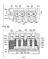
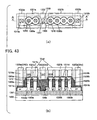
- FIG. 43(a) is a top plan view showing a CMOS inverter according to the sixth embodiment
- FIG. 43(b) is a sectional view taken along the line A-A' in FIG. 43(a) .
- an interconnection layer 1320a connected to an NMOS transistor is connected to GND
- an interconnection layer 1320b connected to a PMOS transistor is connected to Vcc.
- An input signal Vin is input into a gate interconnection layer 1308 from an interconnection layer 1322, and two interconnection lines 1321a, 1321b connected from respective upper sides of the NMOS and PMOS transistors are connected to each other through an interconnection layer to output an output signal Vout therefrom. In this manner, a CMOS inverter is formed.
- CMOS inverter a structure of the CMOS inverter according to the sixth embodiment will be described below.
- Each of two silicon layers 1302a, 1302b on an SOI substrate is electrically isolated on an element-by-element basis.
- Two piitar-shaped silicon layers (pillar-shaped semiconductor layers) 1305a constituting an NMOS transistor (NMOS pillar-shaped silicon layers (NMOS pillar-shaped semiconductor layers) 1305a), and four pillar-shaped silicon layers (pillar-shaped semiconductor layers) 1305b constituting a PMOS transistor (PMOS pillar-shaped silicon layers (PMOS pillar-shaped semiconductor layers) 1305b) are formed on the silicon layer 1302a and silicon layer 1302b, respectively.
- a gate dielectric film (first dielectric film) 1307 and a gate electrode (1308a, 1308b) are formed around each of the pillar-shaped silicon layers (pillar-shaped semiconductor layers).
- a High-k film is used as the gate dielectric film (first dielectric film)
- a metal film is used as the gate electrode.
- a silicon oxynitride film formed by oxidation may be used as the gate dielectric film (first dielectric film), and a polysilicon film may be used as the gate electrode.
- a lower N + diffusion layer (first drain/source diffusion region, i.e., one of drain and source diffusion regions) 1303a is formed underneath the NMOS pillar-shaped silicon layers (NMOS pillar-shaped semiconductor layers) 1305a, and a lower P + diffusion layer (first drain/source diffusion region) 1303b is formed underneath the PMOS pillar-shaped silicon layers (PMOS pillar-shaped semiconductor layers) 1305b.
- a lower silicide layer (1311a, 1311b) is formed on a surface of each of the lower N + and P+ diffusion layers (first drain/source diffusion regions) to reduce a parasitic resistance.
- An upper N + diffusion layer (second drain/source diffusion region, i.e., a remaining one of the drain and source diffusion regions) 1309a is formed on top of each of the NMOS pillar-shaped silicon layers (NMOS pillar-shaped semiconductor layers) 1305a in such a manner that an area of an upper surface thereof becomes greater than that of an upper surface of the NMOS pillar-shaped silicon layer.
- An upper P + diffusion layer (second drain/source diffusion region) 1309b is formed on top of each the PMOS pillar-shaped silicon layers (PMOS pillar-shaped semiconductor layers) 1305b in such a manner that an area of an upper surface thereof becomes greater than that of an upper surface of the PMOS pillar-shaped silicon layer.
- the upper diffusion layer having an upper surface with an area greater than that of the upper surface of the pillar-shaped silicon layer is comprised of an upper portion formed in an epitaxially-grown semiconductor epitaxial layer, and a lower portion formed in an upper portion of the pillar-shaped silicon layer.
- the upper diffusion layer may be formed only in a part or an entirety of the semiconductor epitaxial layer.
- the semiconductor epitaxial layer is electrically isolated from the gate electrode (1308a, 1308b) by a second dielectric film 1312, such as a silicon nitride film or a laminated film comprised of a silicon nitride film and a silicon oxide film, interposed therebetween.
- the two NMOS pillar-shaped silicon layers (NMOS pillar-shaped semiconductor layers) 1305a are arranged adjacent to each other, so that epitaxial silicon layers (semiconductor epitaxial layers) to be formed on tops of respective upper surfaces of the NMOS pillar-shaped silicon layers (NMOS pillar-shaped semiconductor layers) are self-alignedly connected together.
- the four PMOS pillar-shaped silicon layers (PMOS pillar-shaped semiconductor layers) 1305b are also arranged adjacent to each other, so that epitaxial silicon layers (semiconductor epitaxial layers) to be formed on tops of respective upper surfaces of the PMOS pillar-shaped silicon layers (PMOS pillar-shaped semiconductor layers) are self-alignedly connected together in the same manner.
- Two upper silicide layers 1311c, 1311d are formed, respectively, on the integral set of upper N + diffusion layers 1309a and the integral set of upper P + diffusion layers (second drain/source diffusion regions) 1309b.
- Each of the upper silicide layers is formed on the connected epitaxial silicon layers (semiconductor epitaxial layers) each having a diameter greater than that of the pillar-shaped silicon layer (pillar-shaped semiconductor layer).
- the narrow width effect on the upper silicide layer can be reduced.
- an interface area between the upper silicide layer and the integral set of upper diffusion layers (1309a, 1309b) can be set largely, so that an interface resistance between the upper silicide layer and the integral set of upper diffusion layers can be reduced.
- the upper silicide layer (1311c, 1311d) may be formed in an upper surface of the integral set of the upper diffusion layers (second drain/source diffusion regions) to have a diameter greater than a total diameter of a plurality of contacts (1315, 1316) to be formed on an upper side of the adjacent pillar-shaped silicon layers (pillar-shaped semiconductor layers). This makes it possible to prevent a short-circuiting between the contact and the gate electrode even if the contact undergoes overetching during etching for contacts.
- an upper side of the pillar-shaped semiconductor layers may be connected to an interconnection layer via a less number of contacts than the number of the pillar-shaped semiconductor layers, as described in connection with FIGS. 24(a) and 24(b) .
- a contact may be formed on an integral set of upper N + diffusion layers (second drain/source diffusion regions) at a position corresponding to a position between adjacent pillar-shaped silicon layers (pillar-shaped semiconductor layers), as described in connection with FIGS. 24(a) and 24(b) .
- an axis of the contact may be located to intersect with a line segment connecting respective axes of the adjacent pillar-shaped silicon layers (pillar-shaped semiconductor layers) or may be located in a region between the axes of the adjacent pillar-shaped silicon layers (pillar-shaped semiconductor layers).
- the number of contacts can be reduced by this arrangement or an arrangement in a PMOS transistor illustrated in FIGS. 24(a) and 24(b) . This makes it possible to largely set a space between adjacent ones of a plurality of interconnection lines 1320a, 1320b, 1321a, 1321b, 1322so as to facilitate interconnection layout.
- a contact having an area greater than that of other contact in cross-section parallel to a principal surface of a substrate may be formed on an upper side of a plurality of pillar-shaped silicon layers (pillar-shaped semiconductor layers), in a number less than the number of the pillar-shaped semiconductor layers. This makes it possible to reduce a resistance of a contact, and stably form a contact.
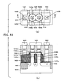
- FIG. 44(a) is a top plan view showing a transistor using a polysilicon layer as a gate electrode, according to a seventh embodiment of the present invention
- FIG. 44(b) is a sectional view taken along the line A-A' in FIG. 44(a) .
- a silicon substrate 1401 is isolated on an element-by-element basis by an element isolation 1402, and two pillar-shaped silicon layers (pillar-shaped semiconductor layers) 1405a, 1405b are formed on the silicon substrate.
- a gate dielectric film (first dielectric film) 1407 and a gate electrode (1408a, 1408b) are formed around each of the pillar-shaped silicon layers (pillar-shaped semiconductor layers).
- a High-k film is used as the gate dielectric film (first dielectric film)
- a polysilicon film is used as the gate electrode.
- a silicon oxynitride film formed by oxidation may be used as the gate dielectric film (first dielectric film).
- a silicide layer 1411c is formed on a surface of the gate electrode, in addition to silicide layers on respective surfaces of after-mentioned diffusion layers.
- a lower N + diffusion layer (first drain/source diffusion region, i.e., one of drain and source diffusion regions) 1403 is formed underneath the pillar-shaped silicon layers (pillar-shaped semiconductor layers), and a lower silicide layer 1411a is formed on a surface of the lower N + diffusion layer (first drain/source diffusion region) 1403, to reduce a parasitic resistance.
- An upper N + diffusion layer (second drain/source diffusion region, i.e., a remaining one of the drain and source diffusion regions) (1409a, 1409b) is formed on top of each of the pillar-shaped silicon layers (pillar-shaped semiconductor layers), in such a manner that an area of an upper surface thereof becomes greater than that of an upper surface of the pillar-shaped silicon layer.
- the upper N + diffusion layer (second drain/source diffusion region) (1409a, 1409b) having an upper surface with an area greater than that of the upper surface of the pillar-shaped silicon layer is comprised of an upper portion formed in an epitaxially-grown semiconductor epitaxial layer, and a lower portion formed in an upper portion of the pillar-shaped silicon layer.
- the upper N + diffusion layer (second drain/source diffusion region) may be formed only in a part or an entirety of the semiconductor epitaxial layer.
- the semiconductor epitaxial layer is electrically isolated from the gate electrode (1408a, 1408b) by a second dielectric film 1412, such as a silicon nitride film or a laminated film comprised of a silicon nitride film and a silicon oxide film, interposed therebetween.
- a distance between the adjacent pillar-shaped silicon layers (pillar-shaped semiconductor layers) 1405a, 1405b is less than a given value.
- a thickness of a film to be epitaxially grown is adjusted in such a manner that the upper N + diffusion layers (second drain/source diffusion regions) on respective ones of the adjacent pillar-shaped semiconductor layers are self-alignedly connected together.
- An upper silicide layer 1411b is formed on the upper N + diffusion layer (second drain/source diffusion region) (1409a, 1409b).
- the upper silicide layer is formed on the epitaxial silicon layer (semiconductor epitaxial layer) having a diameter greater than that of the pillar-shaped silicon layer (pillar-shaped semiconductor layer).
- the narrow width effect on the upper silicide layer can be reduced.
- an interface area between the upper silicide layer and the upper N + diffusion layer can be set largely, so that an interface resistance between the upper silicide layer and the upper N + diffusion layer can be reduced.
- the upper silicide layer (1411b) may be formed in an upper surface of the upper N + diffusion layer (second drain/source diffusion region) to have a diameter greater than that of a contact (1415, 1416) to be formed on an upper side of the pillar-shaped silicon layer (pillar-shaped semiconductor layer). This makes it possible to prevent a short-circuiting between the contact and the gate electrode even if the contact undergoes overetching during etching for contacts.
- the contact (1415, 1416) formed on the upper side of the pillar-shaped silicon layer (pillar-shaped semiconductor layer) is connected to one of drain and source terminals through an interconnection layer 1420.
- a contact 1418 formed on a lower side of the pillar-shaped silicon layer (pillar-shaped semiconductor layer) is connected to a remaining one of the drain and source terminals through an interconnection layer 1422, and a contact 1417 formed on a gate line 1408 extending from the gate electrode is connected to a gate terminal through an interconnection layer 1421.
- a production method for the transistor according to the seventh embodiment is the same as that for the transistor according to the first embodiment. Further, in cases where the transistor according to the seventh embodiment uses an SOI substrate, the same production method as that for the transistor according to the fourth embodiment may be used.
- an upper side of the pillar-shaped semiconductor layers may be connected to an interconnection layer via a less number of contacts than the number of the pillar-shaped semiconductor layers, as described in connection with FIGS. 3(a) and 3(b) .
- a contact may be formed on an integral set of upper N + diffusion layers (second drain/source diffusion regions) at a position corresponding to a position between adjacent pillar-shaped silicon layers (pillar-shaped semiconductor layers), as described in connection with FIGS. 4(a) and 4(b) .
- an axis of the contact may be located to intersect with a line segment connecting respective axes of the adjacent pillar-shaped silicon layers (pillar-shaped semiconductor layers) or may be located in a region between the axes of the adjacent pillar-shaped silicon layers (pillar-shaped semiconductor layers).
- a contact having an area greater than that of other contact in cross-section parallel to a principal surface of a substrate may be formed on an upper side of a plurality of pillar-shaped silicon layers (pillar-shaped semiconductor layers), in a number less than the number of the pillar-shaped semiconductor layers, as described in connection with FIGS. 5(a) and 5(b) . This makes it possible to reduce a resistance of a contact, and stably form a contact.
- FIG. 45(a) is a top plan view showing a transistor having a gate electrode formed of a fully-silicided polysilicon layer, according to an eighth embodiment of the present invention
- FIG. 45(b) is a sectional view taken along the line A-A' in FIG. 45(a) .
- a silicon substrate 1501 is isolated on an element-by-element basis by an element isolation 1502, and two pillar-shaped silicon layers (pillar-shaped semiconductor layers) 1505a, 1505b are formed on the silicon substrate.
- a gate dielectric film (first dielectric film) 1507and a gate electrode (1508a, 1508b) are formed around each of the pillar-shaped silicon layers (pillar-shaped semiconductor layers).
- a High-k film is used as the gate dielectric film (first dielectric film)
- a fully-silicided polysilicon film is used as the gate electrode.
- a silicon oxynitride film formed by oxidation may be used as the gate dielectric film (first dielectric film).
- the polysilicon gate electrode is fully silicided by optimizing a thickness of a sputtered film made of a silicide material or by adjusting siliciding conditions.
- a lower N + diffusion layer (first drain/source diffusion region, i.e., one of drain and source diffusion regions) 1503 is formed underneath the pillar-shaped silicon layers (pillar-shaped semiconductor layers), and a lower silicide layer 1511a is formed on a surface of the lower N + diffusion layer (first drain/source diffusion region) 1503, to reduce a parasitic resistance.
- An upper N + diffusion layer (second drain/source diffusion region, i.e., a remaining one of the drain and source diffusion regions) (1509a, 1509b) is formed on top of each of the pillar-shaped silicon layers (pillar-shaped semiconductor layers), in such a manner that an area of an upper surface thereof becomes greater than that of an upper surface of the pillar-shaped silicon layer.
- the upper N + diffusion layer (second drain/source diffusion region) (1509a, 1509b) having an upper surface with an area greater than that of the upper surface of the pillar-shaped silicon layer is comprised of an upper portion formed in an epitaxially-grown semiconductor epitaxial layer, and a lower portion formed in an upper portion of the pillar-shaped silicon layer.
- the upper N + diffusion layer (second drain/source diffusion region) may be formed only in a part or an entirety of the semiconductor epitaxial layer.
- the semiconductor epitaxial layer is electrically isolated from the gate electrode (1508a, 1508b) by a second dielectric film 1512, such as a silicon nitride film or a laminated film comprised of a silicon nitride film and a silicon oxide film, interposed therebetween.
- a distance between the adjacent pillar-shaped silicon layers (pillar-shaped semiconductor layers) 1505a, 1505b is less than a given value.
- a thickness of a film to be epitaxially grown is adjusted in such a manner that the upper N + diffusion layers (second drain/source diffusion regions) on respective ones of the adjacent pillar-shaped semiconductor layers are self-alignedly connected together.
- An upper silicide layer 1511b is formed on the upper N + diffusion layer (second drain/source diffusion region) (1509a, 1509b).
- the upper silicide layer is formed on the epitaxial silicon layer (semiconductor epitaxial layer) having a diameter greater than that of the pillar-shaped silicon layer (pillar-shaped semiconductor layer).
- the narrow width effect on the upper silicide layer can be reduced.
- an interface area between the upper silicide layer and the upper N + diffusion layer can be set largely, so that an interface resistance between the upper silicide layer and the upper N + diffusion layer can be reduced.
- the upper silicide layer (1511b) may be formed in an upper surface of the upper N + diffusion layer (second drain/source diffusion region) to have a diameter greater than that of a contact (1515, 1516) to be formed on an upper side of the pillar-shaped silicon layer (pillar-shaped semiconductor layer). This makes it possible to prevent a short-circuiting between the contact and the gate electrode even if the contact undergoes overetching during etching for contacts.
- the contact (1515, 1516) formed on the upper side of the pillar-shaped silicon layer (pillar-shaped semiconductor layer) is connected to one of drain and source terminals through an interconnection layer 1520.
- a contact 1518 formed on a lower side of the pillar-shaped silicon layer (pillar-shaped semiconductor layer) is connected to a remaining one of the drain and source terminals through an interconnection layer 1522, and a contact 1517 formed on a gate line 1508 extending from the gate electrode is connected to a gate terminal through an interconnection layer 1521.
- a production method for the transistor according to the eighth embodiment is the same as that for the transistor according to the first embodiment. Further, in cases where the transistor according to the seventh embodiment uses an SOI substrate, the same production method as that for the transistor according to the fourth embodiment may be used.
- an upper side of the pillar-shaped semiconductor layers may be connected to an interconnection layer via a less number of contacts than the number of the pillar-shaped semiconductor layers, as described in connection with FIGS. 3(a) and 3(b) .
- a contact may be formed on an integral set of upper N + diffusion layers (second drain/source diffusion regions) at a position corresponding to a position between adjacent pillar-shaped silicon layers (pillar-shaped semiconductor layers), as described in connection with FIGS. 4(a) and 4(b) .
- an axis of the contact may be located to intersect with a line segment connecting respective axes of the adjacent pillar-shaped silicon layers (pillar-shaped semiconductor layers) or may be located in a region between the axes of the adjacent pillar-shaped silicon layers (pillar-shaped semiconductor layers).
- a contact having an area greater than that of other contact in cross-section parallel to a principal surface of a substrate may be formed on an upper side of a plurality of pillar-shaped silicon layers (pillar-shaped semiconductor layers), in a number less than the number of the pillar-shaped semiconductor layers, as described in connection with FIGS. 5(a) and 5(b) . This makes it possible to reduce a resistance of a contact, and stably form a contact.
Landscapes
- Insulated Gate Type Field-Effect Transistor (AREA)
- Thin Film Transistor (AREA)
- Metal-Oxide And Bipolar Metal-Oxide Semiconductor Integrated Circuits (AREA)
- Electrodes Of Semiconductors (AREA)
Applications Claiming Priority (1)
| Application Number | Priority Date | Filing Date | Title |
|---|---|---|---|
| JP2009109126A JP5317343B2 (ja) | 2009-04-28 | 2009-04-28 | 半導体装置及びその製造方法 |
Publications (2)
| Publication Number | Publication Date |
|---|---|
| EP2246893A2 true EP2246893A2 (de) | 2010-11-03 |
| EP2246893A3 EP2246893A3 (de) | 2012-07-25 |
Family
ID=42338279
Family Applications (1)
| Application Number | Title | Priority Date | Filing Date |
|---|---|---|---|
| EP10004492A Withdrawn EP2246893A3 (de) | 2009-04-28 | 2010-04-28 | Halbleiterbauelement, das einen MOS-Transistor enthält, und Herstellungsverfahren dafür |
Country Status (7)
| Country | Link |
|---|---|
| US (2) | US8497548B2 (de) |
| EP (1) | EP2246893A3 (de) |
| JP (1) | JP5317343B2 (de) |
| KR (2) | KR20100118531A (de) |
| CN (2) | CN105023948A (de) |
| SG (1) | SG166085A1 (de) |
| TW (1) | TWI438900B (de) |
Families Citing this family (110)
| Publication number | Priority date | Publication date | Assignee | Title |
|---|---|---|---|---|
| US8183628B2 (en) | 2007-10-29 | 2012-05-22 | Unisantis Electronics Singapore Pte Ltd. | Semiconductor structure and method of fabricating the semiconductor structure |
| JP5317343B2 (ja) | 2009-04-28 | 2013-10-16 | ユニサンティス エレクトロニクス シンガポール プライベート リミテッド | 半導体装置及びその製造方法 |
| US8598650B2 (en) | 2008-01-29 | 2013-12-03 | Unisantis Electronics Singapore Pte Ltd. | Semiconductor device and production method therefor |
| US8188537B2 (en) | 2008-01-29 | 2012-05-29 | Unisantis Electronics Singapore Pte Ltd. | Semiconductor device and production method therefor |
| JP4487221B1 (ja) * | 2009-04-17 | 2010-06-23 | 日本ユニサンティスエレクトロニクス株式会社 | 半導体装置 |
| JP4577592B2 (ja) | 2009-04-20 | 2010-11-10 | 日本ユニサンティスエレクトロニクス株式会社 | 半導体装置の製造方法 |
| JP5356970B2 (ja) | 2009-10-01 | 2013-12-04 | ユニサンティス エレクトロニクス シンガポール プライベート リミテッド | 半導体装置 |
| TWI416727B (zh) * | 2009-12-04 | 2013-11-21 | 華亞科技股份有限公司 | P型金屬氧化層半導體場效電晶體及其製造方法 |
| JP2011166089A (ja) * | 2010-02-15 | 2011-08-25 | Elpida Memory Inc | 半導体装置及びその製造方法 |
| WO2011111662A1 (ja) | 2010-03-08 | 2011-09-15 | 日本ユニサンティスエレクトロニクス株式会社 | 固体撮像装置 |
| US8487357B2 (en) | 2010-03-12 | 2013-07-16 | Unisantis Electronics Singapore Pte Ltd. | Solid state imaging device having high sensitivity and high pixel density |
| JP5066590B2 (ja) | 2010-06-09 | 2012-11-07 | ユニサンティス エレクトロニクス シンガポール プライベート リミテッド | 半導体装置とその製造方法 |
| JP5087655B2 (ja) | 2010-06-15 | 2012-12-05 | ユニサンティス エレクトロニクス シンガポール プライベート リミテッド | 半導体装置及びその製造方法 |
| US20120168819A1 (en) * | 2011-01-03 | 2012-07-05 | Fabio Alessio Marino | Semiconductor pillar power MOS |
| US9401436B2 (en) | 2011-05-05 | 2016-07-26 | Qualcomm Incorporated | Multiple control transcap variable capacitor |
| KR101227339B1 (ko) * | 2011-05-12 | 2013-01-28 | 에스케이하이닉스 주식회사 | 반도체 소자 및 그 형성 방법 |
| JP2013026382A (ja) * | 2011-07-20 | 2013-02-04 | Elpida Memory Inc | 半導体装置の製造方法 |
| US8564034B2 (en) | 2011-09-08 | 2013-10-22 | Unisantis Electronics Singapore Pte. Ltd. | Solid-state imaging device |
| US8669601B2 (en) | 2011-09-15 | 2014-03-11 | Unisantis Electronics Singapore Pte. Ltd. | Method for producing semiconductor device and semiconductor device having pillar-shaped semiconductor |
| US8759178B2 (en) | 2011-11-09 | 2014-06-24 | Unisantis Electronics Singapore Pte. Ltd. | Method for manufacturing semiconductor device and semiconductor device |
| US10438836B2 (en) | 2011-11-09 | 2019-10-08 | Unisantis Electronics Singapore Pte. Ltd. | Method for manufacturing a semiconductor device |
| JP5596237B2 (ja) * | 2011-12-19 | 2014-09-24 | ユニサンティス エレクトロニクス シンガポール プライベート リミテッド | 半導体装置の製造方法と半導体装置 |
| US8772175B2 (en) | 2011-12-19 | 2014-07-08 | Unisantis Electronics Singapore Pte. Ltd. | Method for manufacturing semiconductor device and semiconductor device |
| US8916478B2 (en) | 2011-12-19 | 2014-12-23 | Unisantis Electronics Singapore Pte. Ltd. | Method for manufacturing semiconductor device and semiconductor device |
| US8748938B2 (en) | 2012-02-20 | 2014-06-10 | Unisantis Electronics Singapore Pte. Ltd. | Solid-state imaging device |
| US9012981B2 (en) | 2012-05-17 | 2015-04-21 | Unisantis Electronics Singapore Pte. Ltd. | Semiconductor device |
| US8829601B2 (en) | 2012-05-17 | 2014-09-09 | Unisantis Electronics Singapore Pte. Ltd. | Semiconductor device |
| US9166043B2 (en) | 2012-05-17 | 2015-10-20 | Unisantis Electronics Singapore Pte. Ltd. | Semiconductor device |
| WO2013171873A1 (ja) * | 2012-05-17 | 2013-11-21 | ユニサンティス エレクトロニクス シンガポール プライベート リミテッド | 半導体装置 |
| KR20140009509A (ko) * | 2012-05-18 | 2014-01-22 | 유니산티스 일렉트로닉스 싱가포르 프라이빗 리미티드 | 반도체 장치의 제조 방법 및 반도체 장치 |
| US8877578B2 (en) | 2012-05-18 | 2014-11-04 | Unisantis Electronics Singapore Pte. Ltd. | Method for producing semiconductor device and semiconductor device |
| US8697511B2 (en) | 2012-05-18 | 2014-04-15 | Unisantis Electronics Singapore Pte. Ltd. | Method for producing semiconductor device and semiconductor device |
| US8829619B2 (en) | 2012-10-09 | 2014-09-09 | Unisantis Electronics Singapore Pte. Ltd. | Method for producing semiconductor device and semiconductor device |
| WO2014057532A1 (ja) * | 2012-10-09 | 2014-04-17 | ユニサンティス エレクトロニクス シンガポール プライベート リミテッド | 半導体装置の製造方法、及び、半導体装置 |
| US20150270268A1 (en) * | 2012-11-06 | 2015-09-24 | Atsushi Fujikawa | Semiconductor device |
| US9000513B2 (en) | 2012-11-12 | 2015-04-07 | Unisantis Electronics Singapore Pte. Ltd. | Method for manufacturing a semiconductor device and semiconductor device with surrounding gate transistor |
| WO2014073103A1 (ja) * | 2012-11-12 | 2014-05-15 | ユニサンティス エレクトロニクス シンガポール プライベート リミテッド | 半導体装置の製造方法、及び、半導体装置 |
| JP5596245B1 (ja) * | 2012-11-12 | 2014-09-24 | ユニサンティス エレクトロニクス シンガポール プライベート リミテッド | 半導体装置の製造方法、及び、半導体装置 |
| US9054215B2 (en) * | 2012-12-18 | 2015-06-09 | Intel Corporation | Patterning of vertical nanowire transistor channel and gate with directed self assembly |
| US8754470B1 (en) * | 2013-01-18 | 2014-06-17 | Taiwan Semiconductor Manufacturing Company, Ltd. | Vertical tunneling field-effect transistor cell and fabricating the same |
| US9041095B2 (en) | 2013-01-24 | 2015-05-26 | Unisantis Electronics Singapore Pte. Ltd. | Vertical transistor with surrounding gate and work-function metal around upper sidewall, and method for manufacturing the same |
| JP5646116B1 (ja) * | 2013-01-24 | 2014-12-24 | ユニサンティス エレクトロニクス シンガポール プライベート リミテッドUnisantis Electronics Singapore Pte Ltd. | 半導体装置の製造方法、及び、半導体装置 |
| US20140264557A1 (en) * | 2013-03-15 | 2014-09-18 | International Business Machines Corporation | Self-aligned approach for drain diffusion in field effect transistors |
| KR20140145777A (ko) | 2013-06-14 | 2014-12-24 | 에스케이하이닉스 주식회사 | 반도체 소자 및 이의 제조 방법 |
| WO2015008387A1 (ja) * | 2013-07-19 | 2015-01-22 | ユニサンティス エレクトロニクス シンガポール プライベート リミテッド | 半導体装置の製造方法、及び、半導体装置 |
| JP5686932B1 (ja) | 2013-07-30 | 2015-03-18 | ユニサンティス エレクトロニクス シンガポール プライベート リミテッドUnisantis Electronics Singapore Pte Ltd. | 半導体装置 |
| WO2015015566A1 (ja) * | 2013-07-30 | 2015-02-05 | ユニサンティス エレクトロニクス シンガポール プライベート リミテッド | 半導体装置 |
| JP5677643B1 (ja) * | 2013-08-08 | 2015-02-25 | ユニサンティス エレクトロニクス シンガポール プライベート リミテッドUnisantis Electronics Singapore Pte Ltd. | 半導体装置 |
| WO2015019469A1 (ja) | 2013-08-08 | 2015-02-12 | ユニサンティス エレクトロニクス シンガポール プライベート リミテッド | 半導体装置 |
| JP5688190B1 (ja) * | 2013-09-03 | 2015-03-25 | ユニサンティス エレクトロニクス シンガポール プライベート リミテッドUnisantis Electronics Singapore Pte Ltd. | 半導体装置 |
| KR20150028419A (ko) * | 2013-09-06 | 2015-03-16 | 에스케이하이닉스 주식회사 | 반도체 장치 및 이의 제조 방법 |
| JP5639317B1 (ja) * | 2013-11-06 | 2014-12-10 | ユニサンティス エレクトロニクス シンガポール プライベート リミテッドUnisantis Electronics Singapore Pte Ltd. | Sgtを有する半導体装置と、その製造方法 |
| US9087897B1 (en) * | 2014-01-31 | 2015-07-21 | International Business Machines Corporation | Semiconductor structures with pair(s) of vertical field effect transistors, each pair having a shared source/drain region and methods of forming the structures |
| WO2015125204A1 (ja) * | 2014-02-18 | 2015-08-27 | ユニサンティス エレクトロニクス シンガポール プライベート リミテッド | 半導体装置の製造方法、及び、半導体装置 |
| JP5838530B1 (ja) * | 2014-03-05 | 2016-01-06 | ユニサンティス エレクトロニクス シンガポール プライベート リミテッドUnisantis Electronics Singapore Pte Ltd. | 半導体装置の製造方法、及び、半導体装置 |
| WO2015132913A1 (ja) * | 2014-03-05 | 2015-09-11 | ユニサンティス エレクトロニクス シンガポール プライベート リミテッド | 半導体装置の製造方法、及び、半導体装置 |
| WO2015147866A1 (en) * | 2014-03-28 | 2015-10-01 | Intel Corporation | Selectively regrown top contact for vertical semiconductor devices |
| US9281363B2 (en) | 2014-04-18 | 2016-03-08 | Taiwan Semiconductor Manufacturing Company Ltd. | Circuits using gate-all-around technology |
| US9755033B2 (en) | 2014-06-13 | 2017-09-05 | Taiwan Semiconductor Manufacturing Co., Ltd. | Semiconductor device and method of forming vertical structure |
| WO2015193940A1 (ja) | 2014-06-16 | 2015-12-23 | ユニサンティス エレクトロニクス シンガポール プライベート リミテッド | 半導体装置の製造方法、及び、半導体装置 |
| JP5990843B2 (ja) * | 2014-07-14 | 2016-09-14 | ユニサンティス エレクトロニクス シンガポール プライベート リミテッドUnisantis Electronics Singapore Pte Ltd. | 半導体装置の製造方法、及び、半導体装置 |
| WO2016013087A1 (ja) * | 2014-07-24 | 2016-01-28 | ユニサンティス エレクトロニクス シンガポール プライベート リミテッド | 半導体装置の製造方法、及び、半導体装置 |
| US9847233B2 (en) * | 2014-07-29 | 2017-12-19 | Taiwan Semiconductor Manufacturing Company Limited | Semiconductor device and formation thereof |
| JP5814437B2 (ja) * | 2014-08-06 | 2015-11-17 | ユニサンティス エレクトロニクス シンガポール プライベート リミテッドUnisantis Electronics Singapore Pte Ltd. | 半導体装置の製造方法と半導体装置 |
| WO2016021020A1 (ja) * | 2014-08-07 | 2016-02-11 | ユニサンティス エレクトロニクス シンガポール プライベート リミテッド | 半導体装置の製造方法、及び、半導体装置 |
| US9985026B2 (en) | 2014-08-15 | 2018-05-29 | Taiwan Semiconductor Manufacturing Co., Ltd. | Transistor, integrated circuit and method of fabricating the same |
| US9893159B2 (en) | 2014-08-15 | 2018-02-13 | Taiwan Semiconductor Manufacturing Co., Ltd. | Transistor, integrated circuit and method of fabricating the same |
| JP6065190B2 (ja) * | 2014-09-05 | 2017-01-25 | ユニサンティス エレクトロニクス シンガポール プライベート リミテッドUnisantis Electronics Singapore Pte Ltd. | 半導体装置 |
| US9373620B2 (en) * | 2014-09-12 | 2016-06-21 | Taiwan Semiconductor Manufacturing Co., Ltd. | Series connected transistor structure and method of manufacturing the same |
| JP5926354B2 (ja) * | 2014-10-31 | 2016-05-25 | ユニサンティス エレクトロニクス シンガポール プライベート リミテッドUnisantis Electronics Singapore Pte Ltd. | 半導体装置 |
| WO2016084205A1 (ja) * | 2014-11-27 | 2016-06-02 | ユニサンティス エレクトロニクス シンガポール プライベート リミテッド | 柱状半導体装置と、その製造方法 |
| US9299835B1 (en) | 2014-12-04 | 2016-03-29 | International Business Machines Corporation | Vertical field effect transistors |
| US9349859B1 (en) | 2015-01-29 | 2016-05-24 | Taiwan Semiconductor Manufacturing Company, Ltd. | Top metal pads as local interconnectors of vertical transistors |
| JP6378826B2 (ja) * | 2015-04-06 | 2018-08-22 | ユニサンティス エレクトロニクス シンガポール プライベート リミテッドUnisantis Electronics Singapore Pte Ltd. | Sgtを有する柱状半導体装置と、その製造方法 |
| US9997463B2 (en) | 2015-07-01 | 2018-06-12 | Stmicroelectronics, Inc. | Modular interconnects for gate-all-around transistors |
| JP5977865B2 (ja) * | 2015-07-03 | 2016-08-24 | ユニサンティス エレクトロニクス シンガポール プライベート リミテッドUnisantis Electronics Singapore Pte Ltd. | 半導体装置の製造方法、及び、半導体装置 |
| US9853163B2 (en) | 2015-09-30 | 2017-12-26 | Stmicroelectronics, Inc. | Gate all around vacuum channel transistor |
| JP6080933B2 (ja) * | 2015-10-28 | 2017-02-15 | ユニサンティス エレクトロニクス シンガポール プライベート リミテッドUnisantis Electronics Singapore Pte Ltd. | 半導体装置 |
| US10121858B2 (en) * | 2015-10-30 | 2018-11-06 | Taiwan Semiconductor Manufacturing Company, Ltd. | Elongated semiconductor structure planarization |
| US9899529B2 (en) | 2015-11-09 | 2018-02-20 | Samsung Electronics Co., Ltd. | Method to make self-aligned vertical field effect transistor |
| US9881872B2 (en) | 2016-01-15 | 2018-01-30 | Taiwan Semiconductor Manufacturing Co., Ltd. | Method for fabricating a local interconnect in a semiconductor device |
| JP6211637B2 (ja) * | 2016-02-01 | 2017-10-11 | ユニサンティス エレクトロニクス シンガポール プライベート リミテッドUnisantis Electronics Singapore Pte Ltd. | 半導体装置の製造方法、及び、半導体装置 |
| US10141426B2 (en) * | 2016-02-08 | 2018-11-27 | International Business Macahines Corporation | Vertical transistor device |
| JP6230648B2 (ja) * | 2016-04-21 | 2017-11-15 | ユニサンティス エレクトロニクス シンガポール プライベート リミテッドUnisantis Electronics Singapore Pte Ltd. | 半導体装置 |
| US10002962B2 (en) | 2016-04-27 | 2018-06-19 | International Business Machines Corporation | Vertical FET structure |
| US9728266B1 (en) | 2016-07-08 | 2017-08-08 | Micron Technology, Inc. | Memory device including multiple select gates and different bias conditions |
| JP6367495B2 (ja) * | 2016-08-18 | 2018-08-01 | ユニサンティス エレクトロニクス シンガポール プライベート リミテッドUnisantis Electronics Singapore Pte Ltd. | 柱状半導体装置とその製造方法 |
| US11088033B2 (en) | 2016-09-08 | 2021-08-10 | International Business Machines Corporation | Low resistance source-drain contacts using high temperature silicides |
| US9859421B1 (en) * | 2016-09-21 | 2018-01-02 | International Business Machines Corporation | Vertical field effect transistor with subway etch replacement metal gate |
| US9991267B1 (en) * | 2017-01-25 | 2018-06-05 | International Business Machines Corporation | Forming eDRAM unit cell with VFET and via capacitance |
| KR102773973B1 (ko) | 2017-02-24 | 2025-03-05 | 삼성전자주식회사 | 반도체 장치 및 이의 제조 방법 |
| US10361300B2 (en) * | 2017-02-28 | 2019-07-23 | International Business Machines Corporation | Asymmetric vertical device |
| CN108735746B (zh) * | 2017-04-13 | 2021-04-06 | 中芯国际集成电路制造(北京)有限公司 | 一种半导体器件及其制造方法和电子装置 |
| JP6953234B2 (ja) * | 2017-08-28 | 2021-10-27 | ラピスセミコンダクタ株式会社 | 半導体装置及び半導体装置の製造方法 |
| JP6978902B2 (ja) * | 2017-11-10 | 2021-12-08 | 富士通株式会社 | 化合物半導体装置、受信機、及び化合物半導体装置の製造方法。 |
| KR102465533B1 (ko) * | 2017-11-21 | 2022-11-11 | 삼성전자주식회사 | 수직 채널을 가지는 반도체 소자 |
| US10381355B2 (en) * | 2018-01-11 | 2019-08-13 | International Business Machines Corporation | Dense vertical field effect transistor structure |
| KR102408526B1 (ko) * | 2018-05-28 | 2022-06-14 | 유니산티스 일렉트로닉스 싱가포르 프라이빗 리미티드 | 주상 반도체 장치와 그 제조 방법 |
| US10930778B2 (en) * | 2018-10-11 | 2021-02-23 | International Business Machines Corporation | Vertical transistor devices with composite high-K and low-K spacers with a controlled top junction |
| WO2020245946A1 (ja) * | 2019-06-05 | 2020-12-10 | ユニサンティス エレクトロニクス シンガポール プライベート リミテッド | 柱状半導体装置の製造方法 |
| DE102019116218A1 (de) * | 2019-06-14 | 2020-12-17 | Infineon Technologies Dresden GmbH & Co. KG | Leistungshalbleitervorrichtung und Verfahren |
| CN112309859B (zh) * | 2019-07-30 | 2023-10-17 | 中芯国际集成电路制造(上海)有限公司 | 半导体结构及其形成方法 |
| CN112397588B (zh) * | 2019-08-15 | 2025-02-21 | 中芯国际集成电路制造(上海)有限公司 | 半导体结构及其形成方法 |
| CN113078216A (zh) * | 2020-01-06 | 2021-07-06 | 中芯国际集成电路制造(上海)有限公司 | 半导体结构及其形成方法 |
| US11177370B2 (en) | 2020-02-28 | 2021-11-16 | International Business Machines Corporation | Vertical field effect transistor with self-aligned source and drain top junction |
| CN113629142B (zh) * | 2020-05-06 | 2023-11-21 | 中芯国际集成电路制造(上海)有限公司 | 半导体结构和半导体结构的形成方法 |
| CN114188412B (zh) * | 2020-09-14 | 2026-01-27 | 中芯国际集成电路制造(上海)有限公司 | 半导体结构及其形成方法 |
| KR20240134992A (ko) * | 2022-06-02 | 2024-09-10 | 양쯔 메모리 테크놀로지스 씨오., 엘티디. | 반도체 구조 및 이를 형성하는 방법 |
| CN117476597A (zh) * | 2022-07-29 | 2024-01-30 | 长江存储科技有限责任公司 | 半导体器件及其制造方法 |
| JP2024049771A (ja) * | 2022-09-29 | 2024-04-10 | 株式会社ジャパンディスプレイ | Cmos回路 |
Citations (1)
| Publication number | Priority date | Publication date | Assignee | Title |
|---|---|---|---|---|
| JPH02188966A (ja) | 1989-01-17 | 1990-07-25 | Toshiba Corp | Mos型半導体装置 |
Family Cites Families (143)
| Publication number | Priority date | Publication date | Assignee | Title |
|---|---|---|---|---|
| US5017977A (en) * | 1985-03-26 | 1991-05-21 | Texas Instruments Incorporated | Dual EPROM cells on trench walls with virtual ground buried bit lines |
| US5258635A (en) * | 1988-09-06 | 1993-11-02 | Kabushiki Kaisha Toshiba | MOS-type semiconductor integrated circuit device |
| JP2804539B2 (ja) * | 1989-09-28 | 1998-09-30 | 沖電気工業株式会社 | 半導体装置およびその製造方法 |
| JPH03187272A (ja) * | 1989-12-15 | 1991-08-15 | Mitsubishi Electric Corp | Mos型電界効果トランジスタ及びその製造方法 |
| EP0510604A3 (de) * | 1991-04-23 | 2001-05-09 | Canon Kabushiki Kaisha | Halbleiteranordnung und Verfahren zu ihrer Herstellung |
| US5208172A (en) * | 1992-03-02 | 1993-05-04 | Motorola, Inc. | Method for forming a raised vertical transistor |
| US5308782A (en) * | 1992-03-02 | 1994-05-03 | Motorola | Semiconductor memory device and method of formation |
| JP2748072B2 (ja) * | 1992-07-03 | 1998-05-06 | 三菱電機株式会社 | 半導体装置およびその製造方法 |
| AU5669794A (en) | 1992-12-11 | 1994-07-04 | Intel Corporation | A mos transistor having a composite gate electrode and method of fabrication |
| JPH06268173A (ja) * | 1993-03-15 | 1994-09-22 | Toshiba Corp | 半導体記憶装置 |
| JP3403231B2 (ja) * | 1993-05-12 | 2003-05-06 | 三菱電機株式会社 | 半導体装置およびその製造方法 |
| JP3745392B2 (ja) * | 1994-05-26 | 2006-02-15 | 株式会社ルネサステクノロジ | 半導体装置 |
| JPH0878533A (ja) * | 1994-08-31 | 1996-03-22 | Nec Corp | 半導体装置及びその製造方法 |
| JP2797984B2 (ja) * | 1994-10-27 | 1998-09-17 | 日本電気株式会社 | 固体撮像素子およびその製造方法 |
| JP3318814B2 (ja) | 1995-03-15 | 2002-08-26 | ソニー株式会社 | 固体撮像装置及びその駆動方法 |
| KR0165398B1 (ko) * | 1995-05-26 | 1998-12-15 | 윤종용 | 버티칼 트랜지스터의 제조방법 |
| JPH098290A (ja) * | 1995-06-20 | 1997-01-10 | Mitsubishi Electric Corp | 半導体装置及びその製造方法 |
| JP3055869B2 (ja) * | 1995-12-15 | 2000-06-26 | 財団法人半導体研究振興会 | 絶縁ゲート型電界効果トランジスタ及びその製造方法 |
| US5767549A (en) * | 1996-07-03 | 1998-06-16 | International Business Machines Corporation | SOI CMOS structure |
| US7052941B2 (en) * | 2003-06-24 | 2006-05-30 | Sang-Yun Lee | Method for making a three-dimensional integrated circuit structure |
| JP4014708B2 (ja) | 1997-08-21 | 2007-11-28 | 株式会社ルネサステクノロジ | 半導体集積回路装置の設計方法 |
| US6242775B1 (en) * | 1998-02-24 | 2001-06-05 | Micron Technology, Inc. | Circuits and methods using vertical complementary transistors |
| JP3467416B2 (ja) * | 1998-04-20 | 2003-11-17 | Necエレクトロニクス株式会社 | 半導体記憶装置及びその製造方法 |
| JP2000039628A (ja) * | 1998-05-16 | 2000-02-08 | Semiconductor Energy Lab Co Ltd | 半導体表示装置 |
| JP3718058B2 (ja) * | 1998-06-17 | 2005-11-16 | 株式会社ルネサステクノロジ | 半導体集積回路装置の製造方法 |
| JP4078721B2 (ja) | 1998-08-24 | 2008-04-23 | ソニー株式会社 | 半導体装置とその製造方法 |
| US6204187B1 (en) | 1999-01-06 | 2001-03-20 | Infineon Technologies North America, Corp. | Contact and deep trench patterning |
| JP2000243085A (ja) | 1999-02-22 | 2000-09-08 | Hitachi Ltd | 半導体装置 |
| JP3621844B2 (ja) | 1999-02-24 | 2005-02-16 | シャープ株式会社 | 増幅型固体撮像装置 |
| JP2000357736A (ja) | 1999-06-15 | 2000-12-26 | Toshiba Corp | 半導体装置及びその製造方法 |
| DE60001601T2 (de) | 1999-06-18 | 2003-12-18 | Lucent Technologies Inc., Murray Hill | Fertigungsverfahren zur Herstellung eines CMOS integrieten Schaltkreises mit vertikalen Transistoren |
| US6392271B1 (en) * | 1999-06-28 | 2002-05-21 | Intel Corporation | Structure and process flow for fabrication of dual gate floating body integrated MOS transistors |
| US6777254B1 (en) | 1999-07-06 | 2004-08-17 | Semiconductor Energy Laboratory Co., Ltd. | Semiconductor device and fabrication method thereof |
| CA2279147C (en) * | 1999-07-29 | 2003-02-18 | Graminia Developments Ltd. | Liquid for producing marker vapour, a method of producing marker vapour and a method of inspection with marker vapour |
| US6483171B1 (en) * | 1999-08-13 | 2002-11-19 | Micron Technology, Inc. | Vertical sub-micron CMOS transistors on (110), (111), (311), (511), and higher order surfaces of bulk, SOI and thin film structures and method of forming same |
| DE19945136A1 (de) | 1999-09-21 | 2001-04-12 | Infineon Technologies Ag | Vertikale Pixelzellen |
| JP2001237421A (ja) | 2000-02-24 | 2001-08-31 | Toshiba Corp | 半導体装置、sramおよびその製造方法 |
| US6882012B2 (en) * | 2000-02-28 | 2005-04-19 | Semiconductor Energy Laboratory Co., Ltd. | Semiconductor device and a method of manufacturing the same |
| JP2002231951A (ja) | 2001-01-29 | 2002-08-16 | Sony Corp | 半導体装置およびその製造方法 |
| US6624459B1 (en) * | 2000-04-12 | 2003-09-23 | International Business Machines Corp. | Silicon on insulator field effect transistors having shared body contact |
| JP3713418B2 (ja) | 2000-05-30 | 2005-11-09 | 光正 小柳 | 3次元画像処理装置の製造方法 |
| JP2001352047A (ja) | 2000-06-05 | 2001-12-21 | Oki Micro Design Co Ltd | 半導体集積回路 |
| JP4021602B2 (ja) | 2000-06-16 | 2007-12-12 | 株式会社東芝 | 半導体記憶装置 |
| JP2002033399A (ja) | 2000-07-13 | 2002-01-31 | Toshiba Corp | 半導体集積回路及びその製造方法 |
| JP4064607B2 (ja) * | 2000-09-08 | 2008-03-19 | 株式会社東芝 | 半導体メモリ装置 |
| US6406962B1 (en) * | 2001-01-17 | 2002-06-18 | International Business Machines Corporation | Vertical trench-formed dual-gate FET device structure and method for creation |
| US6531727B2 (en) * | 2001-02-09 | 2003-03-11 | Micron Technology, Inc. | Open bit line DRAM with ultra thin body transistors |
| US6448601B1 (en) * | 2001-02-09 | 2002-09-10 | Micron Technology, Inc. | Memory address and decode circuits with ultra thin body transistors |
| JP3908911B2 (ja) | 2001-02-16 | 2007-04-25 | シャープ株式会社 | イメージセンサの製造方法 |
| JP3899236B2 (ja) | 2001-02-16 | 2007-03-28 | シャープ株式会社 | イメージセンサの製造方法 |
| FR2823009B1 (fr) * | 2001-04-02 | 2004-07-09 | St Microelectronics Sa | Procede de fabrication d'un transistor vertical a grille isolee a faible recouvrement de la grille sur la source et sur le drain, et circuit integre comportant un tel transistor |
| US6927433B2 (en) * | 2001-06-28 | 2005-08-09 | Isetec, Inc | Active pixel image sensor with two transistor pixel, in-pixel non-uniformity correction, and bootstrapped reset lines |
| JP2003068883A (ja) | 2001-08-24 | 2003-03-07 | Hitachi Ltd | 半導体記憶装置 |
| US6798017B2 (en) * | 2001-08-31 | 2004-09-28 | International Business Machines Corporation | Vertical dual gate field effect transistor |
| US6461900B1 (en) * | 2001-10-18 | 2002-10-08 | Chartered Semiconductor Manufacturing Ltd. | Method to form a self-aligned CMOS inverter using vertical device integration |
| JP2003142684A (ja) | 2001-11-02 | 2003-05-16 | Toshiba Corp | 半導体素子及び半導体装置 |
| US6657259B2 (en) | 2001-12-04 | 2003-12-02 | International Business Machines Corporation | Multiple-plane FinFET CMOS |
| US6670642B2 (en) | 2002-01-22 | 2003-12-30 | Renesas Technology Corporation. | Semiconductor memory device using vertical-channel transistors |
| US6658259B2 (en) | 2002-03-07 | 2003-12-02 | Interwave Communications International, Ltd. | Wireless network having a virtual HLR and method of operating the same |
| JP2004096065A (ja) | 2002-07-08 | 2004-03-25 | Renesas Technology Corp | 半導体記憶装置およびその製造方法 |
| JP2004079694A (ja) | 2002-08-14 | 2004-03-11 | Fujitsu Ltd | スタンダードセル |
| JP4639040B2 (ja) | 2002-10-10 | 2011-02-23 | パナソニック株式会社 | 半導体装置の製造方法 |
| JP2004165462A (ja) * | 2002-11-14 | 2004-06-10 | Sony Corp | 固体撮像素子及びその製造方法 |
| US7138685B2 (en) | 2002-12-11 | 2006-11-21 | International Business Machines Corporation | Vertical MOSFET SRAM cell |
| KR100467027B1 (ko) | 2003-01-07 | 2005-01-24 | 삼성전자주식회사 | 수직 트랜지스터로 구성된 에스램 소자 및 그 제조방법 |
| JP2004259733A (ja) | 2003-02-24 | 2004-09-16 | Seiko Epson Corp | 固体撮像装置 |
| WO2004084228A1 (en) | 2003-03-18 | 2004-09-30 | Kabushiki Kaisha Toshiba | Phase change memory device |
| US6902962B2 (en) * | 2003-04-04 | 2005-06-07 | Taiwan Semiconductor Manufacturing Company, Ltd. | Silicon-on-insulator chip with multiple crystal orientations |
| JP2004319808A (ja) | 2003-04-17 | 2004-11-11 | Takehide Shirato | Mis電界効果トランジスタ及びその製造方法 |
| JP4108537B2 (ja) | 2003-05-28 | 2008-06-25 | 富士雄 舛岡 | 半導体装置 |
| US6943407B2 (en) * | 2003-06-17 | 2005-09-13 | International Business Machines Corporation | Low leakage heterojunction vertical transistors and high performance devices thereof |
| JP4651920B2 (ja) * | 2003-07-15 | 2011-03-16 | ルネサスエレクトロニクス株式会社 | 半導体装置 |
| JP4904815B2 (ja) * | 2003-10-09 | 2012-03-28 | 日本電気株式会社 | 半導体装置及びその製造方法 |
| JP4758061B2 (ja) | 2003-10-16 | 2011-08-24 | パナソニック株式会社 | 固体撮像装置およびその製造方法 |
| JP4416474B2 (ja) | 2003-10-28 | 2010-02-17 | 株式会社ルネサステクノロジ | 半導体記憶装置 |
| US7372091B2 (en) * | 2004-01-27 | 2008-05-13 | Micron Technology, Inc. | Selective epitaxy vertical integrated circuit components |
| US6878991B1 (en) * | 2004-01-30 | 2005-04-12 | Micron Technology, Inc. | Vertical device 4F2 EEPROM memory |
| KR100532564B1 (ko) | 2004-05-25 | 2005-12-01 | 한국전자통신연구원 | 다중 게이트 모스 트랜지스터 및 그 제조 방법 |
| JP4218894B2 (ja) * | 2004-07-08 | 2009-02-04 | シャープ株式会社 | 固体撮像装置およびその製造方法 |
| US7518182B2 (en) * | 2004-07-20 | 2009-04-14 | Micron Technology, Inc. | DRAM layout with vertical FETs and method of formation |
| US7247570B2 (en) * | 2004-08-19 | 2007-07-24 | Micron Technology, Inc. | Silicon pillars for vertical transistors |
| US7442970B2 (en) * | 2004-08-30 | 2008-10-28 | Micron Technology, Inc. | Active photosensitive structure with buried depletion layer |
| US7241655B2 (en) * | 2004-08-30 | 2007-07-10 | Micron Technology, Inc. | Method of fabricating a vertical wrap-around-gate field-effect-transistor for high density, low voltage logic and memory array |
| US7271052B1 (en) * | 2004-09-02 | 2007-09-18 | Micron Technology, Inc. | Long retention time single transistor vertical memory gain cell |
| US8110869B2 (en) * | 2005-02-11 | 2012-02-07 | Alpha & Omega Semiconductor, Ltd | Planar SRFET using no additional masks and layout method |
| JP5017795B2 (ja) | 2005-04-13 | 2012-09-05 | 日本電気株式会社 | 電界効果トランジスタの製造方法 |
| US7371627B1 (en) * | 2005-05-13 | 2008-05-13 | Micron Technology, Inc. | Memory array with ultra-thin etched pillar surround gate access transistors and buried data/bit lines |
| US20060261406A1 (en) | 2005-05-18 | 2006-11-23 | Yijian Chen | Vertical integrated-gate CMOS device and its fabrication process |
| KR100673012B1 (ko) | 2005-09-02 | 2007-01-24 | 삼성전자주식회사 | 이중 게이트형 수직 채널 트랜지스터들을 구비하는다이내믹 랜덤 억세스 메모리 장치 및 그 제조 방법 |
| FR2891664B1 (fr) | 2005-09-30 | 2007-12-21 | Commissariat Energie Atomique | Transistor mos vertical et procede de fabrication |
| KR100800469B1 (ko) * | 2005-10-05 | 2008-02-01 | 삼성전자주식회사 | 매몰 비트 라인에 접속된 수직형 트랜지스터를 포함하는회로 소자 및 제조 방법 |
| US7977736B2 (en) * | 2006-02-23 | 2011-07-12 | Samsung Electronics Co., Ltd. | Vertical channel transistors and memory devices including vertical channel transistors |
| JP2008028240A (ja) * | 2006-07-24 | 2008-02-07 | Toshiba Corp | 固体撮像装置 |
| JP2008053388A (ja) * | 2006-08-23 | 2008-03-06 | Toshiba Corp | 半導体装置及びその製造方法 |
| US8058683B2 (en) * | 2007-01-18 | 2011-11-15 | Samsung Electronics Co., Ltd. | Access device having vertical channel and related semiconductor device and a method of fabricating the access device |
| JP5114968B2 (ja) | 2007-02-20 | 2013-01-09 | 富士通セミコンダクター株式会社 | 半導体装置及びその製造方法 |
| JP2008227026A (ja) * | 2007-03-12 | 2008-09-25 | Toshiba Corp | 半導体装置の製造方法 |
| JP5130596B2 (ja) * | 2007-05-30 | 2013-01-30 | 国立大学法人東北大学 | 半導体装置 |
| JP2009037115A (ja) * | 2007-08-03 | 2009-02-19 | Sony Corp | 半導体装置およびその製造方法、並びに表示装置 |
| WO2009034623A1 (ja) * | 2007-09-12 | 2009-03-19 | Unisantis Electronics (Japan) Ltd. | 固体撮像素子 |
| US8330089B2 (en) * | 2007-09-12 | 2012-12-11 | Unisantis Electronics Singapore Pte Ltd. | Solid-state imaging device |
| US8101500B2 (en) * | 2007-09-27 | 2012-01-24 | Fairchild Semiconductor Corporation | Semiconductor device with (110)-oriented silicon |
| JP2009088134A (ja) * | 2007-09-28 | 2009-04-23 | Elpida Memory Inc | 半導体装置、半導体装置の製造方法並びにデータ処理システム |
| JP4900195B2 (ja) | 2007-10-26 | 2012-03-21 | 大日本印刷株式会社 | オーサリング装置、方法およびコンピュータプログラム |
| US8183628B2 (en) * | 2007-10-29 | 2012-05-22 | Unisantis Electronics Singapore Pte Ltd. | Semiconductor structure and method of fabricating the semiconductor structure |
| WO2009057194A1 (ja) | 2007-10-29 | 2009-05-07 | Unisantis Electronics (Japan) Ltd. | 半導体構造及び当該半導体構造の製造方法 |
| JP2009117518A (ja) * | 2007-11-05 | 2009-05-28 | Toshiba Corp | 半導体記憶装置およびその製造方法 |
| US8896056B2 (en) | 2007-12-05 | 2014-11-25 | Unisantis Electronics Singapore Pte Ltd. | Surrounding gate transistor semiconductor device |
| US7935598B2 (en) * | 2007-12-24 | 2011-05-03 | Hynix Semiconductor Inc. | Vertical channel transistor and method of fabricating the same |
| US7956434B2 (en) * | 2007-12-27 | 2011-06-07 | Dongbu Hitek Co., Ltd. | Image sensor and method for manufacturing the same |
| JP4316658B2 (ja) | 2008-01-29 | 2009-08-19 | 日本ユニサンティスエレクトロニクス株式会社 | 半導体装置の製造方法 |
| US8598650B2 (en) * | 2008-01-29 | 2013-12-03 | Unisantis Electronics Singapore Pte Ltd. | Semiconductor device and production method therefor |
| WO2009095997A1 (ja) | 2008-01-29 | 2009-08-06 | Unisantis Electronics (Japan) Ltd. | 半導体装置およびその製造方法 |
| JP5317343B2 (ja) | 2009-04-28 | 2013-10-16 | ユニサンティス エレクトロニクス シンガポール プライベート リミテッド | 半導体装置及びその製造方法 |
| US8188537B2 (en) * | 2008-01-29 | 2012-05-29 | Unisantis Electronics Singapore Pte Ltd. | Semiconductor device and production method therefor |
| WO2009096001A1 (ja) | 2008-01-29 | 2009-08-06 | Unisantis Electronics (Japan) Ltd. | 半導体記憶装置およびメモリ混載半導体装置、並びにそれらの製造方法 |
| WO2009095998A1 (ja) | 2008-01-29 | 2009-08-06 | Unisantis Electronics (Japan) Ltd. | 半導体記憶装置 |
| US8154086B2 (en) * | 2008-01-29 | 2012-04-10 | Unisantis Electronics Singapore Pte Ltd. | Semiconductor surround gate SRAM storage device |
| US8378425B2 (en) * | 2008-01-29 | 2013-02-19 | Unisantis Electronics Singapore Pte Ltd. | Semiconductor storage device |
| JP4316657B2 (ja) | 2008-01-29 | 2009-08-19 | 日本ユニサンティスエレクトロニクス株式会社 | 半導体装置 |
| US8212298B2 (en) * | 2008-01-29 | 2012-07-03 | Unisantis Electronics Singapore Pte Ltd. | Semiconductor storage device and methods of producing it |
| WO2009096002A1 (ja) | 2008-01-29 | 2009-08-06 | Unisantis Electronics (Japan) Ltd. | 半導体装置の製造方法 |
| WO2009095999A1 (ja) | 2008-01-29 | 2009-08-06 | Unisantis Electronics (Japan) Ltd. | 半導体記憶装置 |
| WO2009101704A1 (ja) | 2008-02-15 | 2009-08-20 | Unisantis Electronics (Japan) Ltd. | 半導体装置の製造方法 |
| WO2009133623A1 (ja) | 2008-05-02 | 2009-11-05 | 日本ユニサンティスエレクトロニクス株式会社 | 固体撮像素子 |
| US8097907B2 (en) * | 2008-05-02 | 2012-01-17 | Unisantis Electronics Singapore Pte Ltd. | Solid-state imaging device |
| KR100971412B1 (ko) | 2008-05-21 | 2010-07-21 | 주식회사 하이닉스반도체 | 반도체 장치의 수직 채널 트랜지스터 형성 방법 |
| JP2010034191A (ja) * | 2008-07-28 | 2010-02-12 | Toshiba Corp | 半導体記憶装置とその製造方法 |
| TWI368315B (en) * | 2008-08-27 | 2012-07-11 | Nanya Technology Corp | Transistor structure, dynamic random access memory containing the transistor structure, and method of making the same |
| JP2010171055A (ja) * | 2009-01-20 | 2010-08-05 | Elpida Memory Inc | 半導体装置およびその製造方法 |
| US8338292B2 (en) * | 2009-02-18 | 2012-12-25 | International Business Machines Corporation | Body contacts for FET in SOI SRAM array |
| TWI388059B (zh) * | 2009-05-01 | 2013-03-01 | Niko Semiconductor Co Ltd | The structure of gold-oxygen semiconductor and its manufacturing method |
| US7968876B2 (en) | 2009-05-22 | 2011-06-28 | Macronix International Co., Ltd. | Phase change memory cell having vertical channel access transistor |
| JP4987926B2 (ja) | 2009-09-16 | 2012-08-01 | ユニサンティス エレクトロニクス シンガポール プライベート リミテッド | 半導体装置 |
| JP2011071235A (ja) | 2009-09-24 | 2011-04-07 | Toshiba Corp | 半導体装置及びその製造方法 |
| KR101116354B1 (ko) * | 2009-09-30 | 2012-03-09 | 주식회사 하이닉스반도체 | 단일측벽콘택에 연결된 매립비트라인을 갖는 반도체장치 및 그제조 방법 |
| JP5356970B2 (ja) | 2009-10-01 | 2013-12-04 | ユニサンティス エレクトロニクス シンガポール プライベート リミテッド | 半導体装置 |
| US8067800B2 (en) * | 2009-12-28 | 2011-11-29 | Force Mos Technology Co., Ltd. | Super-junction trench MOSFET with resurf step oxide and the method to make the same |
| WO2011111662A1 (ja) | 2010-03-08 | 2011-09-15 | 日本ユニサンティスエレクトロニクス株式会社 | 固体撮像装置 |
| JP5054182B2 (ja) | 2010-03-12 | 2012-10-24 | ユニサンティス エレクトロニクス シンガポール プライベート リミテッド | 固体撮像装置 |
| JP5066590B2 (ja) | 2010-06-09 | 2012-11-07 | ユニサンティス エレクトロニクス シンガポール プライベート リミテッド | 半導体装置とその製造方法 |
| JP5087655B2 (ja) | 2010-06-15 | 2012-12-05 | ユニサンティス エレクトロニクス シンガポール プライベート リミテッド | 半導体装置及びその製造方法 |
| US8378400B2 (en) | 2010-10-29 | 2013-02-19 | Unisantis Electronics Singapore Pte Ltd. | Solid state imaging device |
-
2009
- 2009-04-28 JP JP2009109126A patent/JP5317343B2/ja active Active
-
2010
- 2010-04-26 SG SG201002931-2A patent/SG166085A1/en unknown
- 2010-04-27 US US12/768,290 patent/US8497548B2/en active Active
- 2010-04-27 KR KR1020100039178A patent/KR20100118531A/ko not_active Ceased
- 2010-04-28 CN CN201510472710.9A patent/CN105023948A/zh active Pending
- 2010-04-28 EP EP10004492A patent/EP2246893A3/de not_active Withdrawn
- 2010-04-28 TW TW099113443A patent/TWI438900B/zh active
- 2010-04-28 CN CN2010101714354A patent/CN101877353A/zh active Pending
-
2013
- 2013-06-13 US US13/917,040 patent/US8647947B2/en active Active
- 2013-08-29 KR KR1020130103392A patent/KR20130103694A/ko not_active Ceased
Patent Citations (1)
| Publication number | Priority date | Publication date | Assignee | Title |
|---|---|---|---|---|
| JPH02188966A (ja) | 1989-01-17 | 1990-07-25 | Toshiba Corp | Mos型半導体装置 |
Also Published As
| Publication number | Publication date |
|---|---|
| JP5317343B2 (ja) | 2013-10-16 |
| JP2010258345A (ja) | 2010-11-11 |
| KR20100118531A (ko) | 2010-11-05 |
| US20100270611A1 (en) | 2010-10-28 |
| EP2246893A3 (de) | 2012-07-25 |
| US20130273703A1 (en) | 2013-10-17 |
| US8497548B2 (en) | 2013-07-30 |
| CN105023948A (zh) | 2015-11-04 |
| SG166085A1 (en) | 2010-11-29 |
| TWI438900B (zh) | 2014-05-21 |
| KR20130103694A (ko) | 2013-09-24 |
| TW201039443A (en) | 2010-11-01 |
| CN101877353A (zh) | 2010-11-03 |
| US8647947B2 (en) | 2014-02-11 |
Similar Documents
| Publication | Publication Date | Title |
|---|---|---|
| EP2246893A2 (de) | Halbleiterbauelement, das einen MOS-Transistor enthält, und Herstellungsverfahren dafür | |
| JP2010258345A5 (de) | ||
| US9508718B2 (en) | FinFET contact structure and method for forming the same | |
| US8786020B2 (en) | Method of fabricating a semiconductor device including a gate having a plurality of fingers extended over a plurality of isolation regions | |
| US8637936B2 (en) | Metal gate transistor with resistor | |
| US7868395B2 (en) | Metal insulator semiconductor field effect transistor having fin structure | |
| US8471344B2 (en) | Integrated circuit device with series-connected fin-type field effect transistors and integrated voltage equalization and method of forming the device | |
| US8952453B2 (en) | MOSFET formed on an SOI wafer with a back gate | |
| US9530871B1 (en) | Method for fabricating a semiconductor device | |
| US20040212024A1 (en) | Metal oxide semiconductor field effect transistors (MOSFETs) including recessed channel regions and methods of fabricating the same | |
| JP6363895B2 (ja) | 半導体装置の製造方法 | |
| EP2755238A2 (de) | Multigate-Metalloxidhalbleitervorrichtungen und Herstellungsverfahren | |
| EP2701196A2 (de) | Halbleiterbauelement mit geneigter Source-/Drain und zugehörige Verfahren | |
| US20210028168A1 (en) | Parallel structure, method of manufacturing the same, and electronic device including the same | |
| KR102814859B1 (ko) | 반도체 소자 | |
| US11158623B2 (en) | Layout of semiconductor device and method of forming semiconductor device | |
| US7754571B2 (en) | Method for forming a strained channel in a semiconductor device | |
| US20200027877A1 (en) | Semiconductor device including a field effect transistor | |
| CN114597262B (zh) | 半导体装置 | |
| US8198659B2 (en) | Semiconductor device and method for fabricating the same | |
| JP6543392B2 (ja) | 半導体装置 | |
| US9640661B1 (en) | FinFET having a fin and a V-shaped epitaxial layer formed on the top surface of the fin and method for fabricating the same | |
| US20250120127A1 (en) | Integrated circuit device including a pfet with a silicon germanium cladded channel and methods of forming the same | |
| US7638837B2 (en) | Stress enhanced semiconductor device and methods for fabricating same | |
| HK1195396A (en) | Semiconductor devices and fabrication methods |
Legal Events
| Date | Code | Title | Description |
|---|---|---|---|
| PUAI | Public reference made under article 153(3) epc to a published international application that has entered the european phase |
Free format text: ORIGINAL CODE: 0009012 |
|
| AK | Designated contracting states |
Kind code of ref document: A2 Designated state(s): AT BE BG CH CY CZ DE DK EE ES FI FR GB GR HR HU IE IS IT LI LT LU LV MC MK MT NL NO PL PT RO SE SI SK SM TR |
|
| AX | Request for extension of the european patent |
Extension state: AL BA ME RS |
|
| RAP1 | Party data changed (applicant data changed or rights of an application transferred) |
Owner name: UNISANTIS ELECTRONICS SINGAPORE PTE. LTD. |
|
| PUAL | Search report despatched |
Free format text: ORIGINAL CODE: 0009013 |
|
| AK | Designated contracting states |
Kind code of ref document: A3 Designated state(s): AT BE BG CH CY CZ DE DK EE ES FI FR GB GR HR HU IE IS IT LI LT LU LV MC MK MT NL NO PL PT RO SE SI SK SM TR |
|
| AX | Request for extension of the european patent |
Extension state: AL BA ME RS |
|
| RIC1 | Information provided on ipc code assigned before grant |
Ipc: H01L 29/786 20060101ALI20120615BHEP Ipc: H01L 21/84 20060101ALI20120615BHEP Ipc: H01L 29/49 20060101ALN20120615BHEP Ipc: H01L 29/08 20060101ALI20120615BHEP Ipc: H01L 21/8238 20060101ALI20120615BHEP Ipc: H01L 29/78 20060101AFI20120615BHEP Ipc: H01L 21/336 20060101ALI20120615BHEP Ipc: H01L 29/417 20060101ALI20120615BHEP |
|
| 17P | Request for examination filed |
Effective date: 20120821 |
|
| RAP1 | Party data changed (applicant data changed or rights of an application transferred) |
Owner name: UNISANTIS ELECTRONICS SINGAPORE PTE. LTD. |
|
| STAA | Information on the status of an ep patent application or granted ep patent |
Free format text: STATUS: THE APPLICATION HAS BEEN WITHDRAWN |
|
| 18W | Application withdrawn |
Effective date: 20140205 |