EP2365417A2 - Elektronische Vorrichtung und elektronisches System - Google Patents
Elektronische Vorrichtung und elektronisches System Download PDFInfo
- Publication number
- EP2365417A2 EP2365417A2 EP11155724A EP11155724A EP2365417A2 EP 2365417 A2 EP2365417 A2 EP 2365417A2 EP 11155724 A EP11155724 A EP 11155724A EP 11155724 A EP11155724 A EP 11155724A EP 2365417 A2 EP2365417 A2 EP 2365417A2
- Authority
- EP
- European Patent Office
- Prior art keywords
- display
- screen
- display panel
- liquid crystal
- display device
- Prior art date
- Legal status (The legal status is an assumption and is not a legal conclusion. Google has not performed a legal analysis and makes no representation as to the accuracy of the status listed.)
- Ceased
Links
Images




Classifications
-
- G—PHYSICS
- G06—COMPUTING OR CALCULATING; COUNTING
- G06F—ELECTRIC DIGITAL DATA PROCESSING
- G06F3/00—Input arrangements for transferring data to be processed into a form capable of being handled by the computer; Output arrangements for transferring data from processing unit to output unit, e.g. interface arrangements
- G06F3/01—Input arrangements or combined input and output arrangements for interaction between user and computer
- G06F3/03—Arrangements for converting the position or the displacement of a member into a coded form
- G06F3/041—Digitisers, e.g. for touch screens or touch pads, characterised by the transducing means
- G06F3/0412—Digitisers structurally integrated in a display
-
- G—PHYSICS
- G02—OPTICS
- G02F—OPTICAL DEVICES OR ARRANGEMENTS FOR THE CONTROL OF LIGHT BY MODIFICATION OF THE OPTICAL PROPERTIES OF THE MEDIA OF THE ELEMENTS INVOLVED THEREIN; NON-LINEAR OPTICS; FREQUENCY-CHANGING OF LIGHT; OPTICAL LOGIC ELEMENTS; OPTICAL ANALOGUE/DIGITAL CONVERTERS
- G02F1/00—Devices or arrangements for the control of the intensity, colour, phase, polarisation or direction of light arriving from an independent light source, e.g. switching, gating or modulating; Non-linear optics
- G02F1/01—Devices or arrangements for the control of the intensity, colour, phase, polarisation or direction of light arriving from an independent light source, e.g. switching, gating or modulating; Non-linear optics for the control of the intensity, phase, polarisation or colour
- G02F1/13—Devices or arrangements for the control of the intensity, colour, phase, polarisation or direction of light arriving from an independent light source, e.g. switching, gating or modulating; Non-linear optics for the control of the intensity, phase, polarisation or colour based on liquid crystals, e.g. single liquid crystal display cells
- G02F1/133—Constructional arrangements; Operation of liquid crystal cells; Circuit arrangements
- G02F1/13306—Circuit arrangements or driving methods for the control of single liquid crystal cells
- G02F1/13318—Circuits comprising a photodetector
-
- G—PHYSICS
- G02—OPTICS
- G02F—OPTICAL DEVICES OR ARRANGEMENTS FOR THE CONTROL OF LIGHT BY MODIFICATION OF THE OPTICAL PROPERTIES OF THE MEDIA OF THE ELEMENTS INVOLVED THEREIN; NON-LINEAR OPTICS; FREQUENCY-CHANGING OF LIGHT; OPTICAL LOGIC ELEMENTS; OPTICAL ANALOGUE/DIGITAL CONVERTERS
- G02F1/00—Devices or arrangements for the control of the intensity, colour, phase, polarisation or direction of light arriving from an independent light source, e.g. switching, gating or modulating; Non-linear optics
- G02F1/01—Devices or arrangements for the control of the intensity, colour, phase, polarisation or direction of light arriving from an independent light source, e.g. switching, gating or modulating; Non-linear optics for the control of the intensity, phase, polarisation or colour
- G02F1/13—Devices or arrangements for the control of the intensity, colour, phase, polarisation or direction of light arriving from an independent light source, e.g. switching, gating or modulating; Non-linear optics for the control of the intensity, phase, polarisation or colour based on liquid crystals, e.g. single liquid crystal display cells
- G02F1/133—Constructional arrangements; Operation of liquid crystal cells; Circuit arrangements
- G02F1/1333—Constructional arrangements; Manufacturing methods
- G02F1/13338—Input devices, e.g. touch panels
-
- G—PHYSICS
- G06—COMPUTING OR CALCULATING; COUNTING
- G06F—ELECTRIC DIGITAL DATA PROCESSING
- G06F1/00—Details not covered by groups G06F3/00 - G06F13/00 and G06F21/00
- G06F1/26—Power supply means, e.g. regulation thereof
- G06F1/32—Means for saving power
- G06F1/3203—Power management, i.e. event-based initiation of a power-saving mode
-
- G—PHYSICS
- G06—COMPUTING OR CALCULATING; COUNTING
- G06F—ELECTRIC DIGITAL DATA PROCESSING
- G06F1/00—Details not covered by groups G06F3/00 - G06F13/00 and G06F21/00
- G06F1/26—Power supply means, e.g. regulation thereof
- G06F1/32—Means for saving power
- G06F1/3203—Power management, i.e. event-based initiation of a power-saving mode
- G06F1/3234—Power saving characterised by the action undertaken
- G06F1/325—Power saving in peripheral device
- G06F1/3265—Power saving in display device
-
- G—PHYSICS
- G06—COMPUTING OR CALCULATING; COUNTING
- G06F—ELECTRIC DIGITAL DATA PROCESSING
- G06F3/00—Input arrangements for transferring data to be processed into a form capable of being handled by the computer; Output arrangements for transferring data from processing unit to output unit, e.g. interface arrangements
- G06F3/01—Input arrangements or combined input and output arrangements for interaction between user and computer
- G06F3/02—Input arrangements using manually operated switches, e.g. using keyboards or dials
- G06F3/0202—Constructional details or processes of manufacture of the input device
- G06F3/0219—Special purpose keyboards
-
- G—PHYSICS
- G06—COMPUTING OR CALCULATING; COUNTING
- G06F—ELECTRIC DIGITAL DATA PROCESSING
- G06F3/00—Input arrangements for transferring data to be processed into a form capable of being handled by the computer; Output arrangements for transferring data from processing unit to output unit, e.g. interface arrangements
- G06F3/01—Input arrangements or combined input and output arrangements for interaction between user and computer
- G06F3/03—Arrangements for converting the position or the displacement of a member into a coded form
- G06F3/041—Digitisers, e.g. for touch screens or touch pads, characterised by the transducing means
- G06F3/042—Digitisers, e.g. for touch screens or touch pads, characterised by the transducing means by opto-electronic means
-
- G—PHYSICS
- G06—COMPUTING OR CALCULATING; COUNTING
- G06F—ELECTRIC DIGITAL DATA PROCESSING
- G06F3/00—Input arrangements for transferring data to be processed into a form capable of being handled by the computer; Output arrangements for transferring data from processing unit to output unit, e.g. interface arrangements
- G06F3/01—Input arrangements or combined input and output arrangements for interaction between user and computer
- G06F3/03—Arrangements for converting the position or the displacement of a member into a coded form
- G06F3/041—Digitisers, e.g. for touch screens or touch pads, characterised by the transducing means
- G06F3/042—Digitisers, e.g. for touch screens or touch pads, characterised by the transducing means by opto-electronic means
- G06F3/0421—Digitisers, e.g. for touch screens or touch pads, characterised by the transducing means by opto-electronic means by interrupting or reflecting a light beam, e.g. optical touch-screen
-
- G—PHYSICS
- G06—COMPUTING OR CALCULATING; COUNTING
- G06F—ELECTRIC DIGITAL DATA PROCESSING
- G06F3/00—Input arrangements for transferring data to be processed into a form capable of being handled by the computer; Output arrangements for transferring data from processing unit to output unit, e.g. interface arrangements
- G06F3/01—Input arrangements or combined input and output arrangements for interaction between user and computer
- G06F3/048—Interaction techniques based on graphical user interfaces [GUI]
- G06F3/0487—Interaction techniques based on graphical user interfaces [GUI] using specific features provided by the input device, e.g. functions controlled by the rotation of a mouse with dual sensing arrangements, or of the nature of the input device, e.g. tap gestures based on pressure sensed by a digitiser
- G06F3/0488—Interaction techniques based on graphical user interfaces [GUI] using specific features provided by the input device, e.g. functions controlled by the rotation of a mouse with dual sensing arrangements, or of the nature of the input device, e.g. tap gestures based on pressure sensed by a digitiser using a touch-screen or digitiser, e.g. input of commands through traced gestures
- G06F3/04886—Interaction techniques based on graphical user interfaces [GUI] using specific features provided by the input device, e.g. functions controlled by the rotation of a mouse with dual sensing arrangements, or of the nature of the input device, e.g. tap gestures based on pressure sensed by a digitiser using a touch-screen or digitiser, e.g. input of commands through traced gestures by partitioning the display area of the touch-screen or the surface of the digitising tablet into independently controllable areas, e.g. virtual keyboards or menus
-
- G—PHYSICS
- G09—EDUCATION; CRYPTOGRAPHY; DISPLAY; ADVERTISING; SEALS
- G09G—ARRANGEMENTS OR CIRCUITS FOR CONTROL OF INDICATING DEVICES USING STATIC MEANS TO PRESENT VARIABLE INFORMATION
- G09G2310/00—Command of the display device
- G09G2310/04—Partial updating of the display screen
-
- G—PHYSICS
- G09—EDUCATION; CRYPTOGRAPHY; DISPLAY; ADVERTISING; SEALS
- G09G—ARRANGEMENTS OR CIRCUITS FOR CONTROL OF INDICATING DEVICES USING STATIC MEANS TO PRESENT VARIABLE INFORMATION
- G09G2330/00—Aspects of power supply; Aspects of display protection and defect management
- G09G2330/02—Details of power systems and of start or stop of display operation
- G09G2330/021—Power management, e.g. power saving
-
- G—PHYSICS
- G09—EDUCATION; CRYPTOGRAPHY; DISPLAY; ADVERTISING; SEALS
- G09G—ARRANGEMENTS OR CIRCUITS FOR CONTROL OF INDICATING DEVICES USING STATIC MEANS TO PRESENT VARIABLE INFORMATION
- G09G2330/00—Aspects of power supply; Aspects of display protection and defect management
- G09G2330/02—Details of power systems and of start or stop of display operation
- G09G2330/021—Power management, e.g. power saving
- G09G2330/022—Power management, e.g. power saving in absence of operation, e.g. no data being entered during a predetermined time
-
- G—PHYSICS
- G09—EDUCATION; CRYPTOGRAPHY; DISPLAY; ADVERTISING; SEALS
- G09G—ARRANGEMENTS OR CIRCUITS FOR CONTROL OF INDICATING DEVICES USING STATIC MEANS TO PRESENT VARIABLE INFORMATION
- G09G2340/00—Aspects of display data processing
- G09G2340/04—Changes in size, position or resolution of an image
- G09G2340/0407—Resolution change, inclusive of the use of different resolutions for different screen areas
- G09G2340/0435—Change or adaptation of the frame rate of the video stream
-
- G—PHYSICS
- G09—EDUCATION; CRYPTOGRAPHY; DISPLAY; ADVERTISING; SEALS
- G09G—ARRANGEMENTS OR CIRCUITS FOR CONTROL OF INDICATING DEVICES USING STATIC MEANS TO PRESENT VARIABLE INFORMATION
- G09G2354/00—Aspects of interface with display user
-
- Y—GENERAL TAGGING OF NEW TECHNOLOGICAL DEVELOPMENTS; GENERAL TAGGING OF CROSS-SECTIONAL TECHNOLOGIES SPANNING OVER SEVERAL SECTIONS OF THE IPC; TECHNICAL SUBJECTS COVERED BY FORMER USPC CROSS-REFERENCE ART COLLECTIONS [XRACs] AND DIGESTS
- Y02—TECHNOLOGIES OR APPLICATIONS FOR MITIGATION OR ADAPTATION AGAINST CLIMATE CHANGE
- Y02D—CLIMATE CHANGE MITIGATION TECHNOLOGIES IN INFORMATION AND COMMUNICATION TECHNOLOGIES [ICT], I.E. INFORMATION AND COMMUNICATION TECHNOLOGIES AIMING AT THE REDUCTION OF THEIR OWN ENERGY USE
- Y02D10/00—Energy efficient computing, e.g. low power processors, power management or thermal management
Definitions
- the present invention relates to an electronic device having a circuit including a transistor, and also relates to an electronic system.
- the present invention relates to, for example, an electronic device on which an electro-optical device typified by a liquid crystal display panel is mounted as a component.
- Patent Document 1 a technique in which an image is displayed with the use of a display element having memory properties has been actively developed because the technique greatly contributes to a reduction of power consumption.
- a display device provided with a touch sensor has attracted attention.
- the display device provided with a touch sensor is called a touch panel, a touch screen, or the like (hereinafter the display device is also referred to simply as a touch panel).
- a display device provided with an optical touch sensor is mounted is disclosed in Patent Document 2.
- An object of the present invention is to provide a novel electronic device which is configured so that a user can input data by directly or indirectly touching a screen of a display device or by casting a shadow with a finger held over the screen without touching it and can use the input data.
- Another object of the present invention is to provide a display device in which a moving-image mode and a still-image mode which consumes less power can be switched on one display screen automatically or by an operation by a user.
- Another object of the present invention is to provide an electronic system which can be easily operated by a user by hand and can consume low power.
- a user inputs data by visually recognizing a keyboard displayed on a screen and touching a corresponding input position of the keyboard on the screen with a finger or the like. Note that still image display is performed in order to display, without limitation to the keyboard, icons or an area where operation keys are displayed.
- the display device includes a storage medium and a display panel in which a photosensor for detecting touch input performed by a user is included in a pixel portion.
- the display panel displays a keyboard on part of a display screen of the display panel.
- the storage medium stores a program (an application program) for controlling power supplied to a still-image area where the keyboard is displayed.
- the display device includes a storage medium in which a control program for a touch-input function and for switching display, which is used for controlling power supplied to each of a moving-image display area, a still-image display area, and the like on one screen, is stored.
- a transistor which includes an oxide semiconductor layer is used in a pixel portion, a display control circuit, or a sensor control circuit, whereby display quality can be maintained even if a non-operation period of the display control circuit is provided after writing of a still image.
- the frequency of rewriting of display is kept to the minimum by a program so that a still image is displayed on an area of a screen where operation buttons such as touch-input buttons (or a keyboard) are displayed and a moving image is displayed in another area of the screen.
- the display of a keyboard is stopped and a still image is displayed on the entire screen.
- the frequency of rewriting of display can be kept to the minimum by the program; thus, power can be saved.
- a second picture including the input data can be displayed on the display screen.
- one embodiment of the present invention disclosed in this specification is a display device which is configured so that a user can input data by, without limitation to touching a display screen, casting a shadow with a finger held over the display screen without touching it.
- the display device includes a display panel which is provided with a pixel portion including a photosensor and to which data is input by detection of a shadow casted on the display screen with a finger held over the screen without touch; a display control circuit for displaying a keyboard on part of the display screen in accordance with the detection by the photosensor; and a storage medium in which a program for controlling power supplied to a still-image area where the keyboard is displayed.
- the display panel is not particularly limited as long as it includes a photosensor in the pixel portion.
- a transmissive liquid crystal display device or a reflective liquid crystal display device can be used.
- a novel electronic device can be provided which is configured so that a user can input data by directly or indirectly touching a screen of a display device or by casting a shadow with a finger held over the screen without touching it and power can be saved with the use of the input data.
- a display device in which a moving-image mode and a still-image mode which consumes less power can be switched on one display screen automatically or by an operation by a user can be realized.
- a transistor which includes an oxide semiconductor layer is used in a pixel portion, a display control circuit, or a sensor control circuit, whereby display quality can be maintained even if a non-operation period of the display control circuit is provided after writing of a still image. The longer a non-operation period of the display control circuit is, the more power can be saved.
- a process of input operation of a reflective display device taken as an example in which a user makes a keyboard displayed on a screen of a display panel by directly or indirectly touching the screen or by casting a shadow with a finger held over the screen without touching it so that a keyboard is displayed on the screen, and furthermore the user inputs data by directly or indirectly touching an area where a desired key of the keyboard is displayed or by casting a shadow with a finger held over the area of the screen without touching it.
- a transimissive display device including a backlight
- data is input by detection of a bright portion.
- the bright portion is formed when a user directly or indirectly touches a screen of a display panel or holds a finger over the screen without touch, that is, the bright portion is formed by reflection of the backlight from the finger.
- the electronic device includes at least a driver circuit for driving the display panel, a detection circuit for driving a photosensor provided in a pixel portion of the display panel, and a storage medium in which a program or a variety of pieces of data is stored.
- a menu screen a TV picture displayed by reception of an image signal, document data stored in the storage medium in advance, or the like is displayed on the screen of the display panel.
- a program for recognizing the menu screen or the data as the still image and automatically switching the display mode into a power-saving mode is started, and the display panel is driven so that the frequency of rewriting of display can be kept to the minimum.
- the screen is divided into a moving-image display area and a still-image display area
- a program for automatically switching the mode of only the still-image display area into a power-saving mode is started, and the display panel is driven so that the frequency of rewriting of display in the still-image display area can be kept to the minimum.
- the detection circuit for driving the photosensor checks at a regular interval whether or not predetermined touch input is performed.
- the detection circuit for driving the photosensor detects the position of the finger on or over the screen.
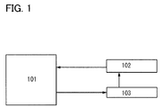
- FIG. 1 illustrates a schematic structure of a display device.
- FIG. 2 illustrates an example of a display screen of the display panel at this stage.
- buttons 11 including a keyboard button 12 and screen scroll buttons 13 are displayed on part of the screen.
- the group of operation buttons 11 is displayed as a still image; thus, a program for recognizing the still image and automatically switching the mode into a power-saving mode is started. Accordingly, the frequency of rewriting of display can be kept to the minimum.
- a program for displaying the group of operation buttons 11 has a value of a display area of the group of operation buttons 11, and thus brings the display control circuit into a non-operation period by using the value.
- the display control circuit is operated to periodically rewrite display.
- the non-operation period of the display control circuit is provided in the area where the operation buttons are displayed, whereby the area is in a power-saving mode.
- the user touches the keyboard button 12 with a finger, indirectly touches the keyboard button 12, or casts a shadow on the screen by holding a finger over the screen without touching it, whereby the display can be switched to keyboard display illustrated in FIG. 3 .
- buttons 21 including keyboard buttons of alphabetical letters and the like and a numerical keypad switch button 22 in addition to the screen scroll buttons are displayed on part of the screen. Needless to say, when the user touches the keyboard buttons of alphabetical letters and the like, alphabetical letters and the like which are input data can be displayed on another part of the screen.
- the group of operation buttons 21 is displayed as a still image; thus, a program for recognizing the still image and automatically switching the mode into a power-saving mode is started. Accordingly, the frequency of rewriting of display can be kept to the minimum.
- the user touches the numerical keypad switch button 22 with a finger, indirectly touches the numerical keypad switch button 22, or casts a shadow on the screen by holding a finger over the screen without touching it, whereby the keyboard display can be switched to display illustrated in FIG. 4 .
- buttons 31 including keyboard buttons of numbers, symbols, and the like and an alphabetical letter switch button 32 in addition to the screen scroll buttons are displayed on part of the screen. Needless to say, when a user touches the keyboard buttons of numbers, symbols, and the like, numbers and symbols which are input data can be displayed on another part of the screen.
- the group of operation buttons 31 is displayed as a still image; thus, a program for recognizing the still image and automatically switching the mode into a power-saving mode is started. Accordingly, the frequency of rewriting of display can be kept to the minimum.
- the display of a keyboard is stopped and a still image is displayed on the entire screen.
- the frequency of rewriting of display can be kept to the minimum by the program; thus, power can be saved.
- a display device in which a moving-image mode and a still-image mode which consumes less power can be switched on one display screen automatically or by an operation by a user can be realized.
- a user when a user performs touch input, the user can slide the display itself by sliding a finger across the screen.
- multi-touch input with two or more fingers without limitation to one finger is also possible. For example, when the user brings two fingers close to each other on the screen, an instruction to zoom out a displayed picture can be given to the electronic device. In addition, when the user brings two fingers away from each other on the screen, an instruction to enlarge a displayed picture can be given to the electronic device.
- liquid crystal panel a transmissive liquid crystal panel in which a photosensor is included in a pixel portion, a reflective liquid crystal panel in which a photosensor is included in a pixel portion, or the like can be used.
- FIG. 5 illustrates a cross-sectional structure of an active matrix substrate in which a photosensor and a transistor are formed over the same substrate.
- FIG. 6 is a top view. A cross-sectional view taken along a chain line A-B in FIG. 6 and a cross-sectional view taken along a chain line C-D in FIG. 6 correspond to FIG. 5 .
- a conductive film is formed over a substrate 230. Then, gate signal lines 213 and 227, a capacitor wiring 224, a photodiode reset signal line 208, a reading signal line, and a photosensor reference signal line are formed through a first photolithography step using a first light-exposure mask.
- a glass substrate is used as the substrate 230.
- An insulating film which serves as a base film may be provided between the substrate 230 and the conductive film.
- the base film has a function of preventing diffusion of impurity elements from the substrate 230.
- the base film can be formed to have a single-layer structure or a stacked-layer structure including one or more of a silicon nitride film, a silicon oxide film, a silicon nitride oxide film, and a silicon oxynitride film.
- the conductive film can be formed to have a single-layer structure or a stacked-layer structure including a metal material such as molybdenum, titanium, tantalum, tungsten, aluminum, copper, neodymium, or scandium, or an alloy material which contains any of these metal materials as its main component.
- a metal material such as molybdenum, titanium, tantalum, tungsten, aluminum, copper, neodymium, or scandium, or an alloy material which contains any of these metal materials as its main component.
- an insulating layer for covering these wirings is formed, and selective etching is performed through a second photolithography step using a second light-exposure mask so that an insulating layer 231 remains only in a portion which intersects with a wiring which is formed later.
- a silicon oxynitride film with a thickness of 600 nm is used as the insulating layer 231.
- a gate insulating layer 232 and an oxide semiconductor film are formed, and a first oxide semiconductor layer 233, a second oxide semiconductor layer, a third oxide semiconductor layer, and a fourth oxide semiconductor layer are formed through a third photolithography step using a third light-exposure mask.
- the first oxide semiconductor layer 233, the second oxide semiconductor layer, the third oxide semiconductor layer, and the fourth oxide semiconductor layer overlap with the gate signal line 227 and the reading signal line with the gate insulating layer 232 interposed therebetween.
- a silicon oxynitride film with a thickness of 100 nm is used as the gate insulating layer 232, and an In-Ga-Zn-O film with a thickness of 30 nm is used as the oxide semiconductor film.
- An oxide thin film represented by a chemical formula of In M O 3 (ZnO) m , ( m >0) can be used for the first oxide semiconductor layer 233, the second oxide semiconductor layer, the third oxide semiconductor layer, and the fourth oxide semiconductor layer.
- M represents one or more metal elements selected from Ga, Al, Mn, and Co.
- M can be Ga, Ga and Al, Ga and Mn, Ga and Co, or the like.
- SiO 2 may be contained in the above oxide thin film.
- an In-Ga-Zn-O film means an oxide film containing indium (In), gallium (Ga), and zinc (Zn), and there is no particular limitation on the stoichiometric proportion.
- the oxide semiconductor layers are subjected to first heat treatment.
- the oxide semiconductor layers can be dehydrated or dehydrogenated by the first heat treatment.
- the temperature of the first heat treatment is higher than or equal to 400 °C and lower than or equal to 750 °C, or higher than or equal to 400 °C and lower than the strain point of the substrate.
- heat treatment is performed with a rapid thermal anneal (RTA) apparatus at 650 °C in a nitrogen atmosphere for six minutes; the substrate is introduced into an electric furnace that is a kind of heat treatment apparatus without being exposed to the air; the oxide semiconductor layers are subjected to heat treatment at 450 °C in a nitrogen atmosphere for one hour; and water or hydrogen is prevented from entering the oxide semiconductor layers; thus, the oxide semiconductor layers can be obtained.
- RTA rapid thermal anneal
- the gate insulating layer 232 is selectively removed through a fourth photolithography step using a fourth light-exposure mask, whereby an opening reaching the gate signal line 213 and an opening reaching the photodiode reset signal line 208 are formed.
- the conductive film can be formed of a metal film containing an element selected from Al, Cr, Cu, Ta, Ti, Mo, and W as its component, an alloy film containing a nitride of any of these elements as its component, an alloy film containing a combination of any of these elements, or the like.
- the conductive film has a three-layer structure in which a Ti film with a thickness of 100 nm, an Al film with a thickness of 400 nm, and a Ti film with a thickness of 100 nm are stacked.
- a resist mask is formed over the conductive film through a fifth photolithography step using a fifth light-exposure mask and selective etching is performed, whereby a video data signal line 210, a photosensor output signal line, and electrode layers 234, 235, and 236 are formed.
- a transistor which includes the first oxide semiconductor layer 233 and the electrode layer 234 which serves as a source electrode layer or a drain electrode layer is manufactured. Further, as illustrated in FIG. 5 , the electrode layer 234, the gate insulating layer 232 serving as a dielectric, and the capacitor wiring 224 form a storage capacitor 222.
- second heat treatment (preferably at higher than or equal to 200 °C and lower than or equal to 400 °C, for example, higher than or equal to 250 °C and lower than or equal to 350 °C) is performed in an inert gas atmosphere or an oxygen gas atmosphere.
- the second heat treatment is performed at 300 °C in a nitrogen atmosphere for one hour.
- part of the oxide semiconductor layer (a channel formation region) is heated while being in contact with the insulating layer.
- an insulating layer 237 which serves as a protective insulating layer is formed, and a sixth photolithography step using a sixth light-exposure mask is performed, whereby an opening reaching the electrode layer 235, an opening reaching the electrode layer 234, and an opening reaching the electrode layer 236 are formed.
- a silicon oxide film with a thickness of 300 nm formed by a sputtering method is used as the insulating layer 237.
- a p layer 238, an i layer 239, and an n layer 240 are stacked by a plasma CVD method.
- a 60 nm thick microcrystalline silicon film containing boron is used as the p layer 238, a 400 nm thick amorphous silicon film is used as the i layer 239, and an 80 nm thick microcrystalline silicon film containing phosphorus is used as the n layer 240.
- the p layer 238, the i layer 239, and the n layer 240 are selectively etched through a seventh photolithography step using a seventh light-exposure mask, and after that part of the n layer 240 and part of the i layer 239 are selectively removed.
- a photosensitive organic resin layer is formed, an eighth photolithography step is performed through which a region to be an opening is exposed to light using an eighth light-exposure mask, and a region to be uneven is exposed to light using a ninth light-exposure mask and developed, whereby an insulating layer 241 which is partly uneven is formed.
- an acrylic resin with a thickness of 1.5 ⁇ m is used for the photosensitive organic resin layer.
- a reflective conductive film is deposited and a ninth photolithography step using a tenth light-exposure mask is performed, whereby a reflective electrode layer 242 and a connection electrode layer 243 are formed.
- the reflective conductive film Al, Ag, or an alloy thereof such as aluminum containing Nd or an Ag-Pd-Cu alloy is used.
- the reflective conductive film is a stacked layer of a 100 nm thick Ti film and a 300 nm thick Al film over the Ti film.
- third heat treatment is performed. In this embodiment, the third heat treatment is performed at 250 °C in a nitrogen atmosphere for one hour.
- a transistor electrically connected to the reflective electrode layer 242 and a photodiode electrically connected to the gate signal line 213 through the connection electrode layer 243 can be formed over one substrate through the nine photolithography steps with the use of the ten light-exposure masks in total.
- Embodiment 1 can be freely combined with Embodiment 1.
- FIG. 8 illustrates a structure of a liquid crystal display module 190.
- the liquid crystal display module 190 includes a display panel 120 in which liquid crystal elements are arranged in matrix, and a polarizing plate and a color filter 115 which overlap with the display panel 120.
- flexible printed circuits (FPCs) 116a and 116b which serve as external input terminals are electrically connected to a terminal portion provided in the display panel 120.
- the display panel 120 has the same structure as the display panel 101 described in Embodiment 1. Note that since the liquid crystal display module 190 performs full-color display, the display panel 120 uses three display elements of a red display element, a green display element, and a blue display element and has a circuit configuration in which different video signals are supplied to the three display elements.
- FIG. 8 schematically illustrates a state in which external light 139 is transmitted through the liquid crystal elements in the display panel 120 and reflected at a reflective electrode.
- the external light 139 is transmitted through the color filter 115 and then passes through the liquid crystal layer, reflected at the reflective electrode, and transmitted again through the color filter 115 to be extracted as red light.
- three colors of light 135 are schematically denoted by arrows (R, G, and B).
- the intensity of the light which is transmitted through the liquid crystal elements is modulated by an image signal; thus, a viewer can perceive an image by reflected light of the external light 139.
- the display panel 120 includes a plurality of photosensors in a pixel portion and has a touch-input function.
- the photosensors can function as visible-light sensors.
- an opening may be provided in the color filter in a region overlapping with the light-receiving region of the photosensor so that the light-receiving region of the photosensor and the color filter do not overlap with each other.
- This embodiment can be freely combined with any of Embodiments 1 and 2.
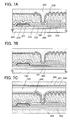
- FIGS. 7A to 7C are cross-sectional process views of the transistor, detailed description on steps and structures of a photodiode and the like, which are the same as those in Embodiment 2, are omitted, and components which are the same as those in FIG. 5 are denoted by the same reference numerals.
- a separation layer 260 is formed over the substrate 230 by a sputtering method, and an oxide insulating film 261 which functions as a base film is formed over the separation layer 260.
- an oxide insulating film 261 which functions as a base film is formed over the separation layer 260.
- a glass substrate, a quartz substrate, or the like is used as the substrate 230.
- the oxide insulating film 261 is formed using a material such as silicon oxide, silicon oxynitride (SiO x N y ) ( x > y >0), or silicon nitride oxide (SiN x O y ) ( x > y >0) by a PCVD method, a sputtering method, or the like.
- a metal film, a stacked layer of a metal film and a metal oxide film, or the like can be used as the separation layer 260.
- the metal film is formed to have a single-layer structure or a stacked-layer structure of a film of an element selected from tungsten (W), molybdenum (Mo), titanium (Ti), tantalum (Ta), niobium (Nb), nickel (Ni), cobalt (Co), zirconium (Zr), zinc (Zn), ruthenium (Ru), rhodium(Rh), palladium (Pd), osmium (Os), and iridium (Ir), or an alloy material or a compound material which contains any of these elements as its main component.
- a metal oxide film of tungsten oxide can be formed on the surface of the tungsten film by performing plasma treatment on the tungsten film.
- a metal film e.g., tungsten
- an insulating film formed of silicon oxide or the like may be formed over the metal film by a sputtering method, and also metal oxide (e.g., tungsten oxide over tungsten) may be formed over the metal film.
- the plasma treatment for example, high-density plasma treatment may be performed with a high-density plasma apparatus.
- a metal nitride film or a metal oxynitride film may be used. In this case, plasma treatment or heat treatment may be performed on the metal film in a nitrogen atmosphere or an atmosphere of nitrogen and oxygen.
- the gate signal line 227, the capacitor wiring 224, the photodiode reset signal line, the reading signal line, and the photosensor reference signal line are formed through a first photolithography step using a first light-exposure mask.
- FIG. 7A is a cross-sectional view illustrating a state at this stage. Note that in FIG. 7A , a cross-sectional structure of the vicinity of the reflective electrode layer 242 is illustrated and a photodiode formed over the same substrate is not illustrated for simplification.
- FIG. 7B is a cross-sectional view illustrating a state at this stage. As illustrated in FIG. 7B , the separation is performed at an interface between the oxide insulating film 261 and the separation layer 260 formed over the substrate 230.
- a flexible substrate 264 is attached to a surface of the layer including the transistor, which is exposed due to the separation, with an adhesive layer 263.
- a plastic film can be used as the flexible substrate 264.
- a thin stainless steel substrate can be used as the flexible substrate 264 because a reflective liquid crystal display device is employed in this embodiment.
- the water-soluble resin layer 262 is removed. After that, an alignment film 244 is formed. Then, a counter substrate 268 provided with a counter electrode 267 is attached to the flexible substrate 264 with a sealant. Note that the counter substrate 268 is also provided with an alignment film 266 for covering the counter electrode 267 before being attached to the flexible substrate 264.
- a liquid crystal dropping method liquid crystal is dropped in a region surrounded by a closed-loop sealant, and a pair of substrates is attached under reduced pressure. In such a manner, a liquid crystal layer 265 fills a region surrounded by the pair of substrates and the sealant.
- the liquid crystal layer 265 There is no particular limitation on the liquid crystal layer 265, and a known liquid crystal material (typically, a nematic liquid crystal material or a cholesteric liquid crystal material) may be used.
- a known liquid crystal material typically, a nematic liquid crystal material or a cholesteric liquid crystal material
- PDLCs polymer dispersed liquid crystals
- PNLCs polymer network liquid crystals
- white display white display
- a polarizing plate is not needed and display close to paper can be realized.
- an eye-friendly liquid crystal display device which causes less eye strain can be manufactured.
- a flexible liquid crystal panel can be manufactured.
- a flexible liquid crystal panel may be manufactured in such a manner that glass substrates used as the substrate 230 and the counter substrate 268 may be processed to be thin by polishing or the like after the transistor is manufactured. In that case, the substrate 230 and the counter substrate 268 are both polished after the liquid crystal layer is formed therebetween.
- liquid crystal panel in which the counter substrate is provided with the counter electrode and an electric field is applied to the liquid crystal layer between the counter electrode and the reflective electrode layer provided for the substrate where the transistor is formed is described in this embodiment.
- a transmissive liquid crystal panel with a lateral electric field method also referred to as IPS
- a pixel electrode layer and a common electrode layer are both provided for a substrate where a transistor is formed, and an electric field is applied to a liquid crystal layer in a direction parallel to the main surface of the substrate, may be manufactured.
- a blue phase liquid crystal without an alignment film may be used to form a transmissive liquid crystal panel.
- a blue phase is one of liquid crystal phases, which is generated just before a cholesteric phase changes into an isotropic phase while temperature of cholesteric liquid crystal is increased. Since the blue phase appears only in a narrow temperature range, a liquid crystal composition containing a chiral agent at 5 wt% or more is used for the liquid crystal layer in order to widen the temperature range.
- the liquid crystal composition containing a liquid crystal exhibiting a blue phase and a chiral agent has a short response time of 1 msec or less and has optical isotropy, which makes the alignment process unneeded, and has a small viewing angle dependence.
- the present invention can be applied to a transmissive liquid crystal panel in which an optical compensate birefringence (OCB) mode is employed.
- OBC optical compensate birefringence
- the response speed of a liquid crystal layer is improved in such a manner that the liquid crystal layer between a pair of substrates is brought into a bend alignment state.
- a pretilt angle of a first alignment film in contact with the liquid crystal layer and a pretilt angle of a second alignment film in contact with the liquid crystal layer are controlled, whereby the bend alignment is made.
- the liquid crystal layer needs to be brought into the bend alignment state from a splay alignment that is an initial state.
- the present invention can be applied to a transmissive liquid crystal panel in which a vertical alignment mode is employed.
- a driving method for achieving a wide viewing angle may be performed in such a manner that one pixel is divided into a plurality of subpixels, and parts of a counter substrate each of which corresponds to the center of each pixel are provided with a projection portion to perform alignment division (multi-domain) of one pixel.
- This driving method is referred to as sub-pixel driving.
- a liquid crystal panel in which a nematic liquid crystal material having negative dielectric anisotropy is used as a liquid crystal material and a vertical alignment film is used as an alignment film may be formed.
- This method in which the vertical alignment film is used is one of voltage control birefringence (also referred to as ECB) methods, and transmittance is controlled utilizing birefringence of liquid crystal molecules.
- ECB voltage control birefringence
- This embodiment can be freely combined with any of Embodiments 1 to 3.
- the liquid crystal display device manufactured through the process described in any of Embodiments 2 to 4 can be applied to a variety of electronic devices (including game machines).
- electronic devices are a television device (also referred to as a television or a television receiver), a monitor of a computer or the like, a camera such as a digital camera or a digital video camera, a digital photo frame, a mobile phone handset (also referred to as a mobile phone or a mobile phone device), a portable game console, a portable information terminal, an audio reproducing device, a large-size game machine such as a pachinko machine, and the like.
- FIG. 9A illustrates an example of a television device.
- a display panel 9603 is incorporated in a housing.
- the display panel 9603 can display images.
- the television device 9601 is fixed to a wall 9600 and is supported at the back of the housing.
- images displayed on the display panel 9603 can be controlled by touch input with the use of a photosensor provided in a pixel portion of the display panel.
- a keyboard can be displayed on the display panel 9603 to input data.
- the television device 9601 can be operated with an operation switch of the housing or a separate remote controller 9610. Channels can be switched and volume can be controlled with operation keys 9609 of the remote controller 9610, whereby an image displayed on the display panel 9603 can be controlled. Further, the remote controller 9610 may be provided with a display panel 9607 for displaying data output from the remote controller 9610.
- the television device 9601 is provided with a receiver, a modem, and the like. With the use of the receiver, general television broadcasting can be received. Moreover, when the display device is connected to a communication network with or without wires via the modem, one-way (from a sender to a receiver) or two-way (between a sender and a receiver, between receivers, or the like) information communication can be performed.
- the display panel 9603 provided with a touch-input function is suitable for one-way or two-way information communication.
- FIG. 9B illustrates a portable game machine including a housing 9881 and a housing 9891, which are jointed with a connector 9893 so that the portable game machine can be opened or folded.
- a display panel 9882 and a display panel 9883 are incorporated in the housing 9881 and the housing 9891, respectively.
- the display panel 9882 and the display panel 9883 each include a photosensor in a pixel portion so that they have touch-input functions.
- the portable game machine illustrated in FIG. 9B has a function of reading a program or data stored in a recording medium to display it on the display panel, and a function of sharing information with another portable game machine by wireless communication.
- FIG. 10A illustrates an example of a mobile phone.
- a mobile phone 1000 includes a display panel 1002 incorporated in a housing 1001, operation buttons 1003, an external connection port 1004, a speaker 1005, a microphone 1006, and the like.
- a user can input data into the mobile phone 1000 illustrated in FIG. 10A by touching the display panel 1002 including a pixel portion having a photosensor with a finger or the like. Further, the user can make a call or text by touching the display panel 1002 with a finger or the like.
- the detection device detects the direction of the mobile phone 1000 (whether the mobile phone 1000 is placed horizontally or vertically for a landscape mode or a portrait mode) so that the screens of the display panel 1002 can be automatically switched.
- the screen modes are switched by touching the display panel 1002 or operating the operation button 1003 of the housing 1001.
- the screen modes can be switched depending on the kind of image displayed on the display panel 1002. For example, when a signal of an image displayed on the display panel is a signal of moving image data, the screen mode is switched to the display mode. When the signal is a signal of text data, the screen mode is switched to the input mode.
- the screen mode when input by touching the display panel 1002 is not performed for a certain period of time while a signal detected by the photosensor provided in the pixel portion of the display panel 1002 is detected, the screen mode may be controlled so as to be switched from the input mode to the display mode.
- FIG. 10B is a perspective view illustrating an example of an e-book reader.
- an e-book reader is opened and includes a plurality of display panels: a first display panel 4311, a second display panel 4312, and a double-sided third display panel between the first display panel 4311 and the second display panel 4312.
- the e-book reader illustrated in FIG. 10B includes the first display panel 4311 including a display panel 4301; the second display panel 4312 including an operation portion 4304 and a display panel 4307; the third display panel 4313 including a display panel 4302 and a display panel 4310; and a binding portion 4308 provided at ends of the first display panel 4311, the second display panel 4312, and the third display panel 4313.
- the third display panel 4313 is interposed between the first display panel 4311 and the second display panel 4312.
- the e-book reader illustrated in FIG. 10B includes four display screens: the display panels 4301, 4307, 4302, and 4310.
- the first display panel 4311, the second display panel 4312, and the third display panel 4313 are flexible and thus are easily bent. These panels can be manufactured by the method described in Embodiment 4.
- the third display panel 4313 is a double-sided display panel including the display panel 4302 and the display panel 4310.
- two liquid crystal display panels between which a backlight (preferably a thin EL light-emitting panel) is interposed are used.
- At least one of the three display panels may perform full-color display and the other display panels may perform monochrome display.
- the second display panel 4312 includes the operation portion 4304 which can have switches for various functions, such as a power switch and a switch for changing display.
- a user can input data into the e-book reader illustrated in FIG. 10B by touching the display panel 4301 or the display panel 4307 in which a photosensor is provided in a pixel portion with a finger, an input pen, or the like, or by operating the operation portion 4304.
- display buttons 4309 are displayed on the display panel 4307, and the user can input data by touching the display button with a finger or the like.
Landscapes
- Engineering & Computer Science (AREA)
- Physics & Mathematics (AREA)
- Theoretical Computer Science (AREA)
- General Engineering & Computer Science (AREA)
- General Physics & Mathematics (AREA)
- Human Computer Interaction (AREA)
- Nonlinear Science (AREA)
- Optics & Photonics (AREA)
- Crystallography & Structural Chemistry (AREA)
- Chemical & Material Sciences (AREA)
- Mathematical Physics (AREA)
- Control Of Indicators Other Than Cathode Ray Tubes (AREA)
- User Interface Of Digital Computer (AREA)
- Controls And Circuits For Display Device (AREA)
- Position Input By Displaying (AREA)
- Input From Keyboards Or The Like (AREA)
- Liquid Crystal (AREA)
- Liquid Crystal Display Device Control (AREA)
- Thin Film Transistor (AREA)
- Devices For Indicating Variable Information By Combining Individual Elements (AREA)
Applications Claiming Priority (1)
| Application Number | Priority Date | Filing Date | Title |
|---|---|---|---|
| JP2010050941 | 2010-03-08 |
Publications (2)
| Publication Number | Publication Date |
|---|---|
| EP2365417A2 true EP2365417A2 (de) | 2011-09-14 |
| EP2365417A3 EP2365417A3 (de) | 2015-04-29 |
Family
ID=43799683
Family Applications (1)
| Application Number | Title | Priority Date | Filing Date |
|---|---|---|---|
| EP20110155724 Ceased EP2365417A3 (de) | 2010-03-08 | 2011-02-24 | Elektronische Vorrichtung und elektronisches System |
Country Status (6)
| Country | Link |
|---|---|
| US (1) | US20110216043A1 (de) |
| EP (1) | EP2365417A3 (de) |
| JP (3) | JP5662841B2 (de) |
| KR (1) | KR20110102210A (de) |
| CN (1) | CN107102760A (de) |
| TW (2) | TW201732525A (de) |
Cited By (4)
| Publication number | Priority date | Publication date | Assignee | Title |
|---|---|---|---|---|
| WO2013089960A1 (en) * | 2011-12-14 | 2013-06-20 | Qualcomm Incorporated | Static image power management |
| US11049468B2 (en) | 2016-03-17 | 2021-06-29 | Semiconductor Energy Laboratory Co., Ltd. | Display device, display module, and electronic device |
| US11074025B2 (en) | 2012-09-03 | 2021-07-27 | Semiconductor Energy Laboratory Co., Ltd. | Display device and method for manufacturing the same |
| WO2022260631A1 (en) * | 2021-06-08 | 2022-12-15 | Kuecuekdumlu Alper | Touch command control card system operating behind a metal surface |
Families Citing this family (22)
| Publication number | Priority date | Publication date | Assignee | Title |
|---|---|---|---|---|
| US20110181616A1 (en) * | 2010-01-26 | 2011-07-28 | Craig Peter Sayers | Graphical effects for an electronic print media viewer |
| US8605059B2 (en) * | 2010-07-02 | 2013-12-10 | Semiconductor Energy Laboratory Co., Ltd. | Input/output device and driving method thereof |
| CN103300639A (zh) * | 2012-03-08 | 2013-09-18 | 程抒一 | 交互式智能电子橱柜 |
| US9134864B2 (en) | 2012-05-31 | 2015-09-15 | Semiconductor Energy Laboratory Co., Ltd. | Electronic device with controller and touch panel for rapid restoration from power-saving mode |
| WO2014044226A1 (zh) * | 2012-09-24 | 2014-03-27 | 艾塔斯科技(镇江)有限公司 | 具有地址管理功能的扫描仪 |
| WO2014077295A1 (en) | 2012-11-15 | 2014-05-22 | Semiconductor Energy Laboratory Co., Ltd. | Liquid crystal display device |
| JPWO2014109264A1 (ja) * | 2013-01-09 | 2017-01-19 | コニカミノルタ株式会社 | タッチパネル用透明電極、タッチパネル、表示装置、およびタッチパネル用透明電極の製造方法 |
| JP5459420B1 (ja) * | 2013-01-31 | 2014-04-02 | 凸版印刷株式会社 | 液晶表示装置及びカラーフィルタ基板 |
| KR102239367B1 (ko) | 2013-11-27 | 2021-04-09 | 가부시키가이샤 한도오따이 에네루기 켄큐쇼 | 터치 패널 |
| US10073571B2 (en) | 2014-05-02 | 2018-09-11 | Semiconductor Energy Laboratory Co., Ltd. | Touch sensor and touch panel including capacitor |
| JP2016066065A (ja) | 2014-09-05 | 2016-04-28 | 株式会社半導体エネルギー研究所 | 表示装置、および電子機器 |
| US9933903B2 (en) * | 2014-10-02 | 2018-04-03 | Semiconductor Energy Laboratory Co., Ltd. | Input device and input/output device |
| US10706790B2 (en) | 2014-12-01 | 2020-07-07 | Semiconductor Energy Laboratory Co., Ltd. | Display device, display module including the display device, and electronic device including the display device or the display module |
| JP2018013765A (ja) | 2016-04-28 | 2018-01-25 | 株式会社半導体エネルギー研究所 | 電子デバイス |
| US10620689B2 (en) | 2016-10-21 | 2020-04-14 | Semiconductor Energy Laboratory Co., Ltd. | Display device, electronic device, and operation method thereof |
| JP2018072821A (ja) | 2016-10-26 | 2018-05-10 | 株式会社半導体エネルギー研究所 | 表示装置およびその動作方法 |
| CN110192239A (zh) | 2017-01-24 | 2019-08-30 | 株式会社半导体能源研究所 | 显示装置及电子设备 |
| CN112955946B (zh) | 2018-11-09 | 2025-05-02 | 株式会社半导体能源研究所 | 显示装置及电子设备 |
| US11302240B2 (en) * | 2019-01-31 | 2022-04-12 | Kunshan yunyinggu Electronic Technology Co., Ltd | Pixel block-based display data processing and transmission |
| CN110007532B (zh) * | 2019-03-29 | 2022-07-01 | 上海天马微电子有限公司 | 显示面板和显示装置 |
| TWI768685B (zh) * | 2021-01-27 | 2022-06-21 | 瑞昱半導體股份有限公司 | 多設定電視選單產生方法與系統 |
| CN114866831B (zh) * | 2021-02-03 | 2024-11-12 | 瑞昱半导体股份有限公司 | 多设定电视选单产生方法与系统 |
Citations (8)
| Publication number | Priority date | Publication date | Assignee | Title |
|---|---|---|---|---|
| JP2001292276A (ja) | 2000-01-31 | 2001-10-19 | Semiconductor Energy Lab Co Ltd | 密着型エリアセンサ及び密着型エリアセンサを備えた表示装置 |
| US20020107055A1 (en) * | 2001-02-07 | 2002-08-08 | Shunpei Yamazaki | Electronic devices |
| JP2006267982A (ja) | 2005-02-28 | 2006-10-05 | Seiko Epson Corp | 電気泳動表示装置の駆動方法 |
| US20070187790A1 (en) * | 2004-10-04 | 2007-08-16 | Hidekazu Takahashi | Semiconductor device and method of manufacturing the same |
| US20090058823A1 (en) * | 2007-09-04 | 2009-03-05 | Apple Inc. | Virtual Keyboards in Multi-Language Environment |
| US20100007632A1 (en) * | 2008-07-10 | 2010-01-14 | Semiconductor Energy Laboratory Co., Ltd. | Semiconductor device |
| US20100007829A1 (en) * | 2008-07-10 | 2010-01-14 | Yoshiaki Oikawa | Liquid crystal display device and method for manufacturing the same |
| JP2010050941A (ja) | 2008-08-21 | 2010-03-04 | Kyocera Kinseki Hertz Corp | 音叉型屈曲水晶振動素子及び水晶振動子並びに水晶発振器 |
Family Cites Families (128)
| Publication number | Priority date | Publication date | Assignee | Title |
|---|---|---|---|---|
| CA1109539A (en) * | 1978-04-05 | 1981-09-22 | Her Majesty The Queen, In Right Of Canada, As Represented By The Ministe R Of Communications | Touch sensitive computer input device |
| JPH04278627A (ja) * | 1991-03-06 | 1992-10-05 | Oki Electric Ind Co Ltd | タッチパネル装置 |
| JPH11505377A (ja) * | 1995-08-03 | 1999-05-18 | フィリップス エレクトロニクス ネムローゼ フェンノートシャップ | 半導体装置 |
| US20020024496A1 (en) * | 1998-03-20 | 2002-02-28 | Hajime Akimoto | Image display device |
| JP3625598B2 (ja) * | 1995-12-30 | 2005-03-02 | 三星電子株式会社 | 液晶表示装置の製造方法 |
| JPH1028777A (ja) * | 1996-07-18 | 1998-02-03 | Sega Enterp Ltd | コントローラ |
| JP2000150861A (ja) * | 1998-11-16 | 2000-05-30 | Tdk Corp | 酸化物薄膜 |
| JP3276930B2 (ja) * | 1998-11-17 | 2002-04-22 | 科学技術振興事業団 | トランジスタ及び半導体装置 |
| JP2000347184A (ja) * | 1999-06-09 | 2000-12-15 | Minolta Co Ltd | 情報表示装置 |
| TW460731B (en) * | 1999-09-03 | 2001-10-21 | Ind Tech Res Inst | Electrode structure and production method of wide viewing angle LCD |
| US6747638B2 (en) * | 2000-01-31 | 2004-06-08 | Semiconductor Energy Laboratory Co., Ltd. | Adhesion type area sensor and display device having adhesion type area sensor |
| JP2001282204A (ja) * | 2000-03-31 | 2001-10-12 | Minolta Co Ltd | 表示装置 |
| JP4178725B2 (ja) * | 2000-06-26 | 2008-11-12 | コニカミノルタホールディングス株式会社 | 電子機器 |
| TW518552B (en) * | 2000-08-18 | 2003-01-21 | Semiconductor Energy Lab | Liquid crystal display device, method of driving the same, and method of driving a portable information device having the liquid crystal display device |
| US7430025B2 (en) * | 2000-08-23 | 2008-09-30 | Semiconductor Energy Laboratory Co., Ltd. | Portable electronic device |
| KR20020038482A (ko) * | 2000-11-15 | 2002-05-23 | 모리시타 요이찌 | 박막 트랜지스터 어레이, 그 제조방법 및 그것을 이용한표시패널 |
| JP3997731B2 (ja) * | 2001-03-19 | 2007-10-24 | 富士ゼロックス株式会社 | 基材上に結晶性半導体薄膜を形成する方法 |
| JP2003005912A (ja) * | 2001-06-20 | 2003-01-10 | Hitachi Ltd | タッチパネル付きディスプレイ装置及び表示方法 |
| JP4090716B2 (ja) * | 2001-09-10 | 2008-05-28 | 雅司 川崎 | 薄膜トランジスタおよびマトリクス表示装置 |
| JP2003098992A (ja) * | 2001-09-19 | 2003-04-04 | Nec Corp | ディスプレイの駆動方法、その回路及び携帯用電子機器 |
| EP1443130B1 (de) * | 2001-11-05 | 2011-09-28 | Japan Science and Technology Agency | Homologer einkristalliner dünner film mit natürlichem supergitter, herstellungsverfahren dafür und vorrichtung, bei der der einkristalline dünne film verwendet wird |
| JP4190862B2 (ja) * | 2001-12-18 | 2008-12-03 | シャープ株式会社 | 表示装置およびその駆動方法 |
| JP4083486B2 (ja) * | 2002-02-21 | 2008-04-30 | 独立行政法人科学技術振興機構 | LnCuO(S,Se,Te)単結晶薄膜の製造方法 |
| US7049190B2 (en) * | 2002-03-15 | 2006-05-23 | Sanyo Electric Co., Ltd. | Method for forming ZnO film, method for forming ZnO semiconductor layer, method for fabricating semiconductor device, and semiconductor device |
| JP3933591B2 (ja) * | 2002-03-26 | 2007-06-20 | 淳二 城戸 | 有機エレクトロルミネッセント素子 |
| US7339187B2 (en) * | 2002-05-21 | 2008-03-04 | State Of Oregon Acting By And Through The Oregon State Board Of Higher Education On Behalf Of Oregon State University | Transistor structures |
| JP2004022625A (ja) * | 2002-06-13 | 2004-01-22 | Murata Mfg Co Ltd | 半導体デバイス及び該半導体デバイスの製造方法 |
| US7105868B2 (en) * | 2002-06-24 | 2006-09-12 | Cermet, Inc. | High-electron mobility transistor with zinc oxide |
| US7067843B2 (en) * | 2002-10-11 | 2006-06-27 | E. I. Du Pont De Nemours And Company | Transparent oxide semiconductor thin film transistors |
| KR100496304B1 (ko) * | 2003-05-01 | 2005-06-17 | 삼성에스디아이 주식회사 | 효율적인 발진기들을 가진 디스플레이 패널의 구동 장치 |
| JP4108633B2 (ja) * | 2003-06-20 | 2008-06-25 | シャープ株式会社 | 薄膜トランジスタおよびその製造方法ならびに電子デバイス |
| US7262463B2 (en) * | 2003-07-25 | 2007-08-28 | Hewlett-Packard Development Company, L.P. | Transistor including a deposited channel region having a doped portion |
| US7295199B2 (en) * | 2003-08-25 | 2007-11-13 | Motorola Inc | Matrix display having addressable display elements and methods |
| WO2005078697A1 (ja) * | 2004-02-17 | 2005-08-25 | Sharp Kabushiki Kaisha | 表示装置およびそれを備えた自動車両 |
| US7282782B2 (en) * | 2004-03-12 | 2007-10-16 | Hewlett-Packard Development Company, L.P. | Combined binary oxide semiconductor device |
| US7145174B2 (en) * | 2004-03-12 | 2006-12-05 | Hewlett-Packard Development Company, Lp. | Semiconductor device |
| US7297977B2 (en) * | 2004-03-12 | 2007-11-20 | Hewlett-Packard Development Company, L.P. | Semiconductor device |
| EP1737044B1 (de) * | 2004-03-12 | 2014-12-10 | Japan Science and Technology Agency | Amorphes oxid und dünnfilmtransistor |
| US7211825B2 (en) * | 2004-06-14 | 2007-05-01 | Yi-Chi Shih | Indium oxide-based thin film transistors and circuits |
| JP2006079589A (ja) * | 2004-08-05 | 2006-03-23 | Sanyo Electric Co Ltd | タッチパネル |
| JP2006100760A (ja) * | 2004-09-02 | 2006-04-13 | Casio Comput Co Ltd | 薄膜トランジスタおよびその製造方法 |
| US7285501B2 (en) * | 2004-09-17 | 2007-10-23 | Hewlett-Packard Development Company, L.P. | Method of forming a solution processed device |
| US7298084B2 (en) * | 2004-11-02 | 2007-11-20 | 3M Innovative Properties Company | Methods and displays utilizing integrated zinc oxide row and column drivers in conjunction with organic light emitting diodes |
| US7829444B2 (en) * | 2004-11-10 | 2010-11-09 | Canon Kabushiki Kaisha | Field effect transistor manufacturing method |
| KR100998527B1 (ko) * | 2004-11-10 | 2010-12-07 | 고쿠리츠다이가쿠호진 토쿄고교 다이가꾸 | 비정질 산화물 및 전계 효과 트랜지스터 |
| RU2358354C2 (ru) * | 2004-11-10 | 2009-06-10 | Кэнон Кабусики Кайся | Светоизлучающее устройство |
| US7791072B2 (en) * | 2004-11-10 | 2010-09-07 | Canon Kabushiki Kaisha | Display |
| EP1815530B1 (de) * | 2004-11-10 | 2021-02-17 | Canon Kabushiki Kaisha | Feldeffekttransistor mit einem amorphen oxid |
| US7453065B2 (en) * | 2004-11-10 | 2008-11-18 | Canon Kabushiki Kaisha | Sensor and image pickup device |
| US7863611B2 (en) * | 2004-11-10 | 2011-01-04 | Canon Kabushiki Kaisha | Integrated circuits utilizing amorphous oxides |
| JP4134008B2 (ja) * | 2004-11-19 | 2008-08-13 | 任天堂株式会社 | 画像処理装置および画像処理プログラム |
| US7579224B2 (en) * | 2005-01-21 | 2009-08-25 | Semiconductor Energy Laboratory Co., Ltd. | Method for manufacturing a thin film semiconductor device |
| TWI481024B (zh) * | 2005-01-28 | 2015-04-11 | 半導體能源研究所股份有限公司 | 半導體裝置,電子裝置,和半導體裝置的製造方法 |
| TWI505473B (zh) * | 2005-01-28 | 2015-10-21 | 半導體能源研究所股份有限公司 | 半導體裝置,電子裝置,和半導體裝置的製造方法 |
| US7858451B2 (en) * | 2005-02-03 | 2010-12-28 | Semiconductor Energy Laboratory Co., Ltd. | Electronic device, semiconductor device and manufacturing method thereof |
| US7948171B2 (en) * | 2005-02-18 | 2011-05-24 | Semiconductor Energy Laboratory Co., Ltd. | Light emitting device |
| US20060197092A1 (en) * | 2005-03-03 | 2006-09-07 | Randy Hoffman | System and method for forming conductive material on a substrate |
| US8681077B2 (en) * | 2005-03-18 | 2014-03-25 | Semiconductor Energy Laboratory Co., Ltd. | Semiconductor device, and display device, driving method and electronic apparatus thereof |
| US7544967B2 (en) * | 2005-03-28 | 2009-06-09 | Massachusetts Institute Of Technology | Low voltage flexible organic/transparent transistor for selective gas sensing, photodetecting and CMOS device applications |
| US7645478B2 (en) * | 2005-03-31 | 2010-01-12 | 3M Innovative Properties Company | Methods of making displays |
| US8300031B2 (en) * | 2005-04-20 | 2012-10-30 | Semiconductor Energy Laboratory Co., Ltd. | Semiconductor device comprising transistor having gate and drain connected through a current-voltage conversion element |
| JP2006344849A (ja) * | 2005-06-10 | 2006-12-21 | Casio Comput Co Ltd | 薄膜トランジスタ |
| US7402506B2 (en) * | 2005-06-16 | 2008-07-22 | Eastman Kodak Company | Methods of making thin film transistors comprising zinc-oxide-based semiconductor materials and transistors made thereby |
| US7691666B2 (en) * | 2005-06-16 | 2010-04-06 | Eastman Kodak Company | Methods of making thin film transistors comprising zinc-oxide-based semiconductor materials and transistors made thereby |
| US7507618B2 (en) * | 2005-06-27 | 2009-03-24 | 3M Innovative Properties Company | Method for making electronic devices using metal oxide nanoparticles |
| KR100711890B1 (ko) * | 2005-07-28 | 2007-04-25 | 삼성에스디아이 주식회사 | 유기 발광표시장치 및 그의 제조방법 |
| JP2007059128A (ja) * | 2005-08-23 | 2007-03-08 | Canon Inc | 有機el表示装置およびその製造方法 |
| JP4280736B2 (ja) * | 2005-09-06 | 2009-06-17 | キヤノン株式会社 | 半導体素子 |
| JP4850457B2 (ja) * | 2005-09-06 | 2012-01-11 | キヤノン株式会社 | 薄膜トランジスタ及び薄膜ダイオード |
| JP2007073705A (ja) * | 2005-09-06 | 2007-03-22 | Canon Inc | 酸化物半導体チャネル薄膜トランジスタおよびその製造方法 |
| JP5116225B2 (ja) * | 2005-09-06 | 2013-01-09 | キヤノン株式会社 | 酸化物半導体デバイスの製造方法 |
| EP1998373A3 (de) * | 2005-09-29 | 2012-10-31 | Semiconductor Energy Laboratory Co, Ltd. | Halbleitervorrichtung mit Halbleiter-Oxidschicht und Herstellungsverfahren dafür |
| JP5037808B2 (ja) * | 2005-10-20 | 2012-10-03 | キヤノン株式会社 | アモルファス酸化物を用いた電界効果型トランジスタ、及び該トランジスタを用いた表示装置 |
| CN101577231B (zh) * | 2005-11-15 | 2013-01-02 | 株式会社半导体能源研究所 | 半导体器件及其制造方法 |
| TWI292281B (en) * | 2005-12-29 | 2008-01-01 | Ind Tech Res Inst | Pixel structure of active organic light emitting diode and method of fabricating the same |
| US7867636B2 (en) * | 2006-01-11 | 2011-01-11 | Murata Manufacturing Co., Ltd. | Transparent conductive film and method for manufacturing the same |
| JP4977478B2 (ja) * | 2006-01-21 | 2012-07-18 | 三星電子株式会社 | ZnOフィルム及びこれを用いたTFTの製造方法 |
| US7576394B2 (en) * | 2006-02-02 | 2009-08-18 | Kochi Industrial Promotion Center | Thin film transistor including low resistance conductive thin films and manufacturing method thereof |
| US7977169B2 (en) * | 2006-02-15 | 2011-07-12 | Kochi Industrial Promotion Center | Semiconductor device including active layer made of zinc oxide with controlled orientations and manufacturing method thereof |
| KR20070101595A (ko) * | 2006-04-11 | 2007-10-17 | 삼성전자주식회사 | ZnO TFT |
| US20070252928A1 (en) * | 2006-04-28 | 2007-11-01 | Toppan Printing Co., Ltd. | Structure, transmission type liquid crystal display, reflection type display and manufacturing method thereof |
| EP2259172A3 (de) * | 2006-06-09 | 2011-04-13 | Apple Inc. | Touchscreen-Flüssigkristallanzeige |
| JP5028033B2 (ja) * | 2006-06-13 | 2012-09-19 | キヤノン株式会社 | 酸化物半導体膜のドライエッチング方法 |
| KR100846497B1 (ko) * | 2006-06-26 | 2008-07-17 | 삼성전자주식회사 | 디스플레이 버튼 입력 장치 및 이를 구비한 휴대용전자장치 |
| JP4714904B2 (ja) * | 2006-07-14 | 2011-07-06 | エプソンイメージングデバイス株式会社 | 電気光学装置およびこれを備える電子機器 |
| JP4609797B2 (ja) * | 2006-08-09 | 2011-01-12 | Nec液晶テクノロジー株式会社 | 薄膜デバイス及びその製造方法 |
| JP4999400B2 (ja) * | 2006-08-09 | 2012-08-15 | キヤノン株式会社 | 酸化物半導体膜のドライエッチング方法 |
| JP4332545B2 (ja) * | 2006-09-15 | 2009-09-16 | キヤノン株式会社 | 電界効果型トランジスタ及びその製造方法 |
| JP5164357B2 (ja) * | 2006-09-27 | 2013-03-21 | キヤノン株式会社 | 半導体装置及び半導体装置の製造方法 |
| JP4274219B2 (ja) * | 2006-09-27 | 2009-06-03 | セイコーエプソン株式会社 | 電子デバイス、有機エレクトロルミネッセンス装置、有機薄膜半導体装置 |
| US7679610B2 (en) * | 2006-09-28 | 2010-03-16 | Honeywell International Inc. | LCD touchscreen panel with external optical path |
| JP2008096523A (ja) * | 2006-10-06 | 2008-04-24 | Hitachi Displays Ltd | 表示装置 |
| JP2008097172A (ja) * | 2006-10-10 | 2008-04-24 | Sony Corp | 表示装置および表示方法 |
| US7622371B2 (en) * | 2006-10-10 | 2009-11-24 | Hewlett-Packard Development Company, L.P. | Fused nanocrystal thin film semiconductor and method |
| US8094129B2 (en) * | 2006-11-27 | 2012-01-10 | Microsoft Corporation | Touch sensing using shadow and reflective modes |
| US7772021B2 (en) * | 2006-11-29 | 2010-08-10 | Samsung Electronics Co., Ltd. | Flat panel displays comprising a thin-film transistor having a semiconductive oxide in its channel and methods of fabricating the same for use in flat panel displays |
| JP2008140684A (ja) * | 2006-12-04 | 2008-06-19 | Toppan Printing Co Ltd | カラーelディスプレイおよびその製造方法 |
| JP5105842B2 (ja) * | 2006-12-05 | 2012-12-26 | キヤノン株式会社 | 酸化物半導体を用いた表示装置及びその製造方法 |
| US8514165B2 (en) * | 2006-12-28 | 2013-08-20 | Semiconductor Energy Laboratory Co., Ltd. | Semiconductor device |
| KR101303578B1 (ko) * | 2007-01-05 | 2013-09-09 | 삼성전자주식회사 | 박막 식각 방법 |
| US8207063B2 (en) * | 2007-01-26 | 2012-06-26 | Eastman Kodak Company | Process for atomic layer deposition |
| KR100851215B1 (ko) * | 2007-03-14 | 2008-08-07 | 삼성에스디아이 주식회사 | 박막 트랜지스터 및 이를 이용한 유기 전계 발광표시장치 |
| US7795613B2 (en) * | 2007-04-17 | 2010-09-14 | Toppan Printing Co., Ltd. | Structure with transistor |
| KR101325053B1 (ko) * | 2007-04-18 | 2013-11-05 | 삼성디스플레이 주식회사 | 박막 트랜지스터 기판 및 이의 제조 방법 |
| KR20080094300A (ko) * | 2007-04-19 | 2008-10-23 | 삼성전자주식회사 | 박막 트랜지스터 및 그 제조 방법과 박막 트랜지스터를포함하는 평판 디스플레이 |
| KR101334181B1 (ko) * | 2007-04-20 | 2013-11-28 | 삼성전자주식회사 | 선택적으로 결정화된 채널층을 갖는 박막 트랜지스터 및 그제조 방법 |
| WO2008133345A1 (en) * | 2007-04-25 | 2008-11-06 | Canon Kabushiki Kaisha | Oxynitride semiconductor |
| KR101345376B1 (ko) * | 2007-05-29 | 2013-12-24 | 삼성전자주식회사 | ZnO 계 박막 트랜지스터 및 그 제조방법 |
| JP5567770B2 (ja) * | 2007-09-21 | 2014-08-06 | 株式会社ジャパンディスプレイ | 表示装置及び表示装置の製造方法 |
| US20100320457A1 (en) * | 2007-11-22 | 2010-12-23 | Masahito Matsubara | Etching solution composition |
| JP2009135188A (ja) * | 2007-11-29 | 2009-06-18 | Sony Corp | 光センサーおよび表示装置 |
| US20090141004A1 (en) * | 2007-12-03 | 2009-06-04 | Semiconductor Energy Laboratory Co., Ltd. | Display device and method for manufacturing the same |
| US8202365B2 (en) * | 2007-12-17 | 2012-06-19 | Fujifilm Corporation | Process for producing oriented inorganic crystalline film, and semiconductor device using the oriented inorganic crystalline film |
| JPWO2009087756A1 (ja) * | 2008-01-07 | 2011-05-26 | 富士通株式会社 | 表示装置及びその駆動方法 |
| EP2085861A1 (de) * | 2008-01-29 | 2009-08-05 | Research In Motion Limited | Elektronische Vorrichtung und Touchscreen-Anzeige |
| JP4645658B2 (ja) * | 2008-02-18 | 2011-03-09 | ソニー株式会社 | センシング装置、表示装置、電子機器およびセンシング方法 |
| JP2009224595A (ja) * | 2008-03-17 | 2009-10-01 | Fujifilm Corp | 有機電界発光表示装置及びその製造方法 |
| KR101925772B1 (ko) * | 2008-07-10 | 2018-12-06 | 가부시키가이샤 한도오따이 에네루기 켄큐쇼 | 발광 장치 및 전자 기기 |
| US8822995B2 (en) * | 2008-07-24 | 2014-09-02 | Samsung Display Co., Ltd. | Display substrate and method of manufacturing the same |
| EP2151811A3 (de) * | 2008-08-08 | 2010-07-21 | Semiconductor Energy Laboratory Co, Ltd. | Anzeigevorrichtung und elektronische Vorrichtung |
| JP5501583B2 (ja) * | 2008-08-08 | 2014-05-21 | 株式会社半導体エネルギー研究所 | 光電変換装置、及び当該光電変換装置を具備する電子機器 |
| JP4623179B2 (ja) * | 2008-09-18 | 2011-02-02 | ソニー株式会社 | 薄膜トランジスタおよびその製造方法 |
| US8866698B2 (en) * | 2008-10-01 | 2014-10-21 | Pleiades Publishing Ltd. | Multi-display handheld device and supporting system |
| JP5451280B2 (ja) * | 2008-10-09 | 2014-03-26 | キヤノン株式会社 | ウルツ鉱型結晶成長用基板およびその製造方法ならびに半導体装置 |
| US9552154B2 (en) * | 2008-11-25 | 2017-01-24 | Samsung Electronics Co., Ltd. | Device and method for providing a user interface |
| KR101097309B1 (ko) * | 2009-05-06 | 2011-12-23 | 삼성모바일디스플레이주식회사 | 터치 동작 인식 방법 및 장치 |
| US20100295821A1 (en) * | 2009-05-20 | 2010-11-25 | Tom Chang | Optical touch panel |
| KR101264727B1 (ko) * | 2009-09-24 | 2013-05-15 | 엘지디스플레이 주식회사 | 터치 패널 내장형 액정 표시 장치 |
-
2011
- 2011-02-24 EP EP20110155724 patent/EP2365417A3/de not_active Ceased
- 2011-02-24 TW TW106116326A patent/TW201732525A/zh unknown
- 2011-02-24 TW TW100106195A patent/TWI594173B/zh not_active IP Right Cessation
- 2011-02-25 JP JP2011039822A patent/JP5662841B2/ja active Active
- 2011-02-28 US US13/036,157 patent/US20110216043A1/en not_active Abandoned
- 2011-03-08 KR KR1020110020273A patent/KR20110102210A/ko not_active Ceased
- 2011-03-08 CN CN201611000043.5A patent/CN107102760A/zh active Pending
-
2014
- 2014-12-05 JP JP2014246387A patent/JP2015092360A/ja not_active Withdrawn
-
2016
- 2016-11-21 JP JP2016226130A patent/JP2017084375A/ja not_active Withdrawn
Patent Citations (8)
| Publication number | Priority date | Publication date | Assignee | Title |
|---|---|---|---|---|
| JP2001292276A (ja) | 2000-01-31 | 2001-10-19 | Semiconductor Energy Lab Co Ltd | 密着型エリアセンサ及び密着型エリアセンサを備えた表示装置 |
| US20020107055A1 (en) * | 2001-02-07 | 2002-08-08 | Shunpei Yamazaki | Electronic devices |
| US20070187790A1 (en) * | 2004-10-04 | 2007-08-16 | Hidekazu Takahashi | Semiconductor device and method of manufacturing the same |
| JP2006267982A (ja) | 2005-02-28 | 2006-10-05 | Seiko Epson Corp | 電気泳動表示装置の駆動方法 |
| US20090058823A1 (en) * | 2007-09-04 | 2009-03-05 | Apple Inc. | Virtual Keyboards in Multi-Language Environment |
| US20100007632A1 (en) * | 2008-07-10 | 2010-01-14 | Semiconductor Energy Laboratory Co., Ltd. | Semiconductor device |
| US20100007829A1 (en) * | 2008-07-10 | 2010-01-14 | Yoshiaki Oikawa | Liquid crystal display device and method for manufacturing the same |
| JP2010050941A (ja) | 2008-08-21 | 2010-03-04 | Kyocera Kinseki Hertz Corp | 音叉型屈曲水晶振動素子及び水晶振動子並びに水晶発振器 |
Non-Patent Citations (3)
| Title |
|---|
| BRIAN ROSS MCFARLANE: "Amorphous Oxide Semiconductors in Circuit Applications", THESIS SUBMITTED TO OREGON STATE UNIVERSITY, 24 September 2008 (2008-09-24), XP055325011, Retrieved from the Internet <URL:http://ir.library.oregonstate.edu/xmlui/bitstream/handle/1957/9529/thesis_final.pdf> [retrieved on 20161201] * |
| JAE KYEONG JEONG ET AL: "A New Era of Oxide Thin-Film Transistors for Large-Sized AMOLED Displays", SID 2008, 15 September 2008 (2008-09-15), XP055324991, Retrieved from the Internet <URL:https://sites.ualberta.ca/~chung3/papers/2008_ID.pdf> [retrieved on 20161201] * |
| TOSHIO KAMIYA ET AL: "Material characteristics and applications of transparent amorphous oxide semiconductors", NPG ASIA MATERIALS, vol. 2, no. 1, 1 January 2010 (2010-01-01), JP, pages 15 - 22, XP055373773, ISSN: 1884-4049, DOI: 10.1038/asiamat.2010.5 * |
Cited By (5)
| Publication number | Priority date | Publication date | Assignee | Title |
|---|---|---|---|---|
| WO2013089960A1 (en) * | 2011-12-14 | 2013-06-20 | Qualcomm Incorporated | Static image power management |
| US10082860B2 (en) | 2011-12-14 | 2018-09-25 | Qualcomm Incorporated | Static image power management |
| US11074025B2 (en) | 2012-09-03 | 2021-07-27 | Semiconductor Energy Laboratory Co., Ltd. | Display device and method for manufacturing the same |
| US11049468B2 (en) | 2016-03-17 | 2021-06-29 | Semiconductor Energy Laboratory Co., Ltd. | Display device, display module, and electronic device |
| WO2022260631A1 (en) * | 2021-06-08 | 2022-12-15 | Kuecuekdumlu Alper | Touch command control card system operating behind a metal surface |
Also Published As
| Publication number | Publication date |
|---|---|
| US20110216043A1 (en) | 2011-09-08 |
| TW201203080A (en) | 2012-01-16 |
| TW201732525A (zh) | 2017-09-16 |
| JP2011210242A (ja) | 2011-10-20 |
| JP5662841B2 (ja) | 2015-02-04 |
| CN102193228A (zh) | 2011-09-21 |
| JP2015092360A (ja) | 2015-05-14 |
| EP2365417A3 (de) | 2015-04-29 |
| CN107102760A (zh) | 2017-08-29 |
| TWI594173B (zh) | 2017-08-01 |
| KR20110102210A (ko) | 2011-09-16 |
| JP2017084375A (ja) | 2017-05-18 |
Similar Documents
| Publication | Publication Date | Title |
|---|---|---|
| EP2365417A2 (de) | Elektronische Vorrichtung und elektronisches System | |
| US10324492B2 (en) | Smartphone with front camera and maximized display screen | |
| JP5878997B2 (ja) | 電子機器 | |
| JP2024147575A (ja) | 半導体装置 | |
| JP6109890B2 (ja) | 電子機器 | |
| TWI539418B (zh) | 顯示裝置及其驅動方法 | |
| US10528079B2 (en) | Data processing device, display method, input/output method, server system, and computer program | |
| US20080204418A1 (en) | Adaptable User Interface and Mechanism for a Portable Electronic Device | |
| US20080204417A1 (en) | Multimodal Adaptive User Interface for a Portable Electronic Device | |
| US9502440B2 (en) | Display device and electronic device | |
| US20080207254A1 (en) | Multimodal Adaptive User Interface for a Portable Electronic Device | |
| CN104007867B (zh) | 具有与触摸传感器整合在一起的显示模块的电子装置 | |
| US20090284481A1 (en) | Devices and Methods for a Backlight to Illuminate Both a Main Display and Morphable Keys or Indicators | |
| US10180605B2 (en) | Display device and method for manufacturing the same | |
| US20090122017A1 (en) | Mobile electronic device having capacitive sensor with reduced visibility isolation areas and corresponding method | |
| JP2002006293A (ja) | 電子機器 | |
| CN101622590A (zh) | 用于便携式电子设备的可适配用户接口和机制 | |
| CN102193228B (zh) | 电子装置和电子系统 |
Legal Events
| Date | Code | Title | Description |
|---|---|---|---|
| PUAI | Public reference made under article 153(3) epc to a published international application that has entered the european phase |
Free format text: ORIGINAL CODE: 0009012 |
|
| AK | Designated contracting states |
Kind code of ref document: A2 Designated state(s): AL AT BE BG CH CY CZ DE DK EE ES FI FR GB GR HR HU IE IS IT LI LT LU LV MC MK MT NL NO PL PT RO RS SE SI SK SM TR |
|
| AX | Request for extension of the european patent |
Extension state: BA ME |
|
| PUAL | Search report despatched |
Free format text: ORIGINAL CODE: 0009013 |
|
| AK | Designated contracting states |
Kind code of ref document: A3 Designated state(s): AL AT BE BG CH CY CZ DE DK EE ES FI FR GB GR HR HU IE IS IT LI LT LU LV MC MK MT NL NO PL PT RO RS SE SI SK SM TR |
|
| AX | Request for extension of the european patent |
Extension state: BA ME |
|
| RIC1 | Information provided on ipc code assigned before grant |
Ipc: G09G 3/36 20060101ALI20150324BHEP Ipc: G02F 1/133 20060101ALI20150324BHEP Ipc: G06F 1/32 20060101AFI20150324BHEP Ipc: G02F 1/1333 20060101ALI20150324BHEP Ipc: G06F 3/048 20130101ALI20150324BHEP Ipc: G06F 3/041 20060101ALI20150324BHEP |
|
| 17P | Request for examination filed |
Effective date: 20151020 |
|
| RBV | Designated contracting states (corrected) |
Designated state(s): AL AT BE BG CH CY CZ DE DK EE ES FI FR GB GR HR HU IE IS IT LI LT LU LV MC MK MT NL NO PL PT RO RS SE SI SK SM TR |
|
| 17Q | First examination report despatched |
Effective date: 20160225 |
|
| APBK | Appeal reference recorded |
Free format text: ORIGINAL CODE: EPIDOSNREFNE |
|
| APBN | Date of receipt of notice of appeal recorded |
Free format text: ORIGINAL CODE: EPIDOSNNOA2E |
|
| APBR | Date of receipt of statement of grounds of appeal recorded |
Free format text: ORIGINAL CODE: EPIDOSNNOA3E |
|
| APAF | Appeal reference modified |
Free format text: ORIGINAL CODE: EPIDOSCREFNE |
|
| APBT | Appeal procedure closed |
Free format text: ORIGINAL CODE: EPIDOSNNOA9E |
|
| STAA | Information on the status of an ep patent application or granted ep patent |
Free format text: STATUS: THE APPLICATION HAS BEEN REFUSED |
|
| 18R | Application refused |
Effective date: 20210728 |